
HT23C040
CMOS 512K ′8-Bit Mask ROM
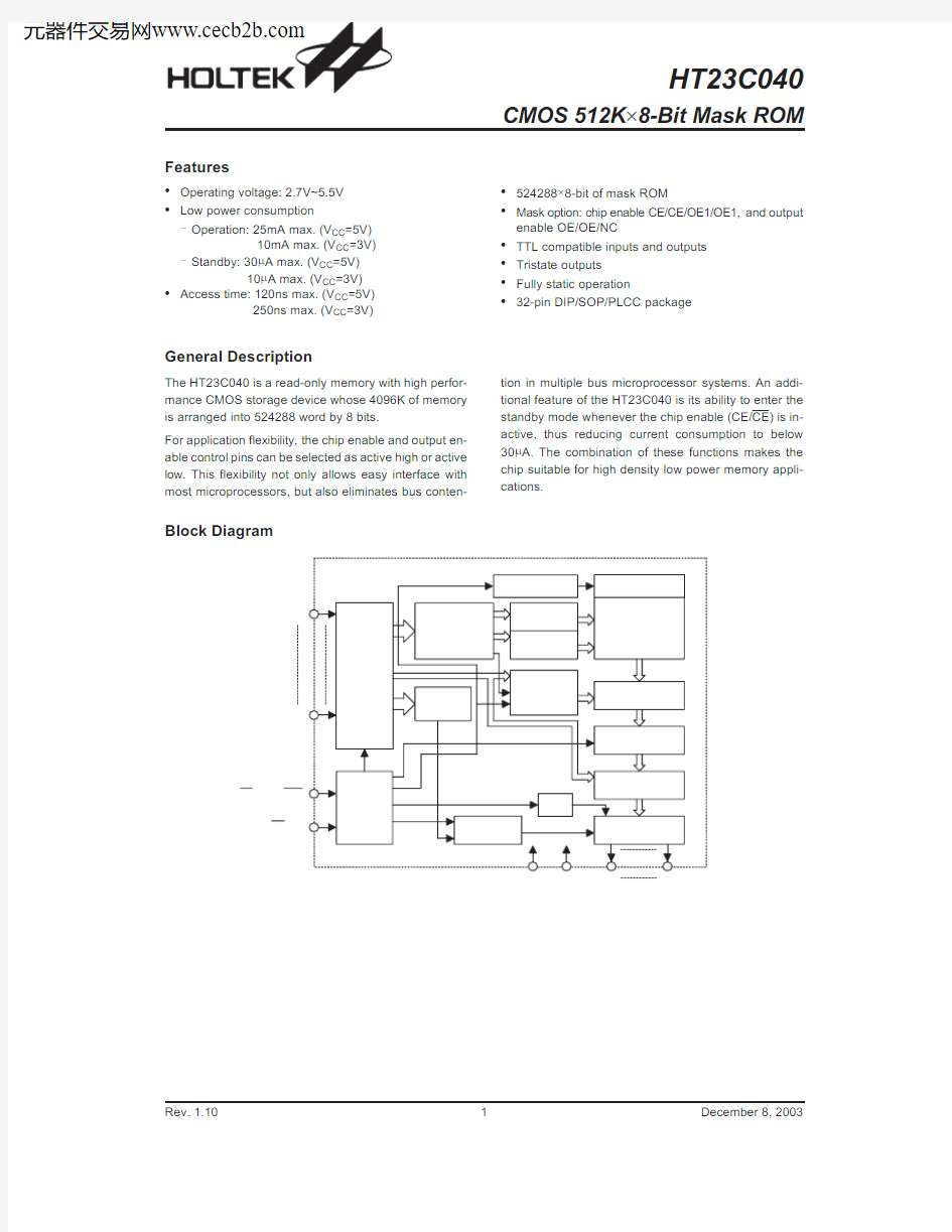
Block Diagram
Rev.1.101December 8,2003
Features
·Operating voltage:2.7V~5.5V ·Low power consumption
-Operation:25mA max.(V CC =5V)
10mA max.(V CC =3V)
-Standby:30m A max.(V CC =5V)
10m A max.(V CC =3V)
·Access time:120ns max.(V CC =5V)
250ns max.(V CC =3V)
·524288′8-bit of mask ROM
·Mask option:chip enable and output
enable ·TTL compatible inputs and outputs ·Tristate outputs ·Fully static operation
·32-pin DIP/SOP/PLCC package
General Description
The HT23C040is a read-only memory with high perfor-mance CMOS storage device whose 4096K of memory is arranged into 524288word by 8bits.
For application flexibility,the chip enable and output en-able control pins can be selected as active high or active low.This flexibility not only allows easy interface with most microprocessors,but also eliminates bus conten-tion in multiple bus microprocessor systems.An addi-tional feature of the HT23C040is its ability to enter the standby mode whenever the chip enable (CE/CE)is in-active,thus reducing current consumption to below 30m A.The combination of these functions makes the chip suitable for high density low power memory appli-
cations.
Pin Assignment
Pin Description
Pin Name I/O Description
NC?No connection
A0~A18I Address inputs
D0~D7O Data outputs
VSS?Negative power supply,ground
CE/CE/OE1/OE1I Chip enable/Output enable input
OE/OE/NC I Output enable input
VCC?Positive power supply
Absolute Maximum Ratings
Supply Voltage..............................V SS-0.3V to V CC+6V Storage Temperature............................-50°C to125°C Input Voltage..............................V SS-0.3V to V CC+0.3V Operating Temperature...........................-40°C to85°C
Note:These are stress ratings only.Stresses exceeding the range specified under2Absolute Maximum Ratings2may cause substantial damage to the device.Functional operation of this device at other conditions beyond those listed in the specification is not implied and prolonged exposure to extreme conditions may affect device reliabil-ity.
Rev.1.102December8,2003
D.C.Characteristics T
a=-40°C to85°C
Symbol Parameter
Test Conditions
Min.Typ.Max.Unit V CC Conditions
Supply Voltage:4.5V~5.5V
V CC Operating Voltage?? 4.5? 5.5V
I CC1Operating Current5V O/P No load,
f=5MHz
??25mA
V IL1Input Low Voltage5V?V SS?0.8V V IH1Input High Voltage5V? 2.2?V CC V V OL1Output Low Voltage5V I OL=3.2mA??0.4V V OH1Output High Voltage5V I OH=-1mA 2.4?V CC V I LI Input Leakage Current5V V IN=0to V CC??10m A I LO Output Leakage Current5V V OUT=0to V CC??10m A I STB1Standby Current5V CE=V IL,CE=V IH?? 1.5mA
I STB2Standby Current5V CE£0.2V
CE3V CC-0.2V
??30m A
C IN Input Capacitance(See note)?f=1MHz??10pF C OUT Output Capacitance(See note)?f=1MHz??10pF Supply Voltage:2.7V~3.3V
V CC Operating Voltage?? 2.7? 3.3V
I CC2Operating Current3V O/P No load,
f=5MHz
??10mA
V IL2Input Low Voltage3V?V SS?0.4V V IH2Input High Voltage3V? 1.5?V CC V
V OL2Output Low Voltage3V I OL=2mA??0.4V V OH2Output High Voltage3V I OH=-0.6mA 1.5?V CC V
I LI Input Leakage Current3V V IN=0to V CC??10m A
I LO Output Leakage Current3V V OUT=0to V CC??10m A
C IN Input Capacitance(See Note)?f=1MHz??10pF
C OUT Output Capacitance(See Note)?f=1MHz??10pF Note:These parameters are periodically sampled but not100%tested.
A.C.Characteristics T
a=-40°C to85°C
Symbol Parameter
3V±10%5V±10%
Unit Min.Max.Min.Max.
t CYC Cycle Time200?120?ns t AA Address Access Time?250?120ns t ACE Chip Enable Access Time?250?120ns t AOE Output Enable Access Time?150?80ns t OH Output Hold Time??10?ns t OD Output Disable Time(See Note)???70ns t OE Output Enable Time(See Note)??10?ns Note:These parameters are periodically sampled but not100%tested.
Rev.1.103December8,2003
A.C.Test Condition Output load:see figure right Input rise and fall time:10ns Input pulse levels:0.4V to 2.4V
Input and output timing reference levels:
0.8V and 2.0V (V CC =5V)1.5V (V CC =3V)
Operation Truth Table
Mode CE/CE OE/OE A0~A18D0~D7Read H/L H/L Valid Data Out Deselect H/L L/H X High Z Standby
L/H
X
X
High Z
Note:H=V IH ,L=V IL ,X=V IH or V IL
Timing Diagrams
Random Read
Rev.1.104December 8,
2003
Output Load Circuit
Functional Description
The HT23C040has two modes,namely data read mode and standby mode,controlled by CE/CE/OE1/OE1and OE/OE/NC inputs.
·Standby mode
The HT23C040offers lower current consumption,controlled by the chip enable input (CE/CE).When a low/high level is applied to the CE/CE input regardless of the output enable (OE/OE/NC)states the chip will enter the standby mode.·Data read mode
When both the chip enable (CE/CE/OE1/OE1)and the output enable (OE/OE/NC)are active,the chip is in data read mode.Otherwise,active CE/CE and inac-tive OE/OE/NC result in deselect mode.The output will remain in Hi-Z state.
Rev.1.105December8,2003
Rev.1.106December8,2003
HT23C040Mask ROM Ordering Sheet Custom:
Input Medium:
EPROM DISK File(Mail Address:romfile@https://www.doczj.com/doc/9918030861.html,)OTHER
User No.Type/https://www.doczj.com/doc/9918030861.html, Q¢ty Check Sum Memory Address Start End
Control Pin and Package Form Option:
(a)32Pin Type Pin22:(1)CE(2)CE(3)OE1(4)OE1
Pin24:(1)OE(2)OE(3)NC
(b)Package Form:(1)Chip Form(2)32DIP(3)32SOP
Companion User No.
Package Marking:
Delivery Date:Q¢ty:
CUSTOM CONFIRMED BY:
(NAME,DATE,POSITION&CO.CHOP)
HOLTEK CONFIRMED BY:
(SALES)(SALES MANAGER)
Rev.1.107December8,2003
Package Information
32-pin DIP(600mil)Outline Dimensions
Symbol
Dimensions in mil
Min.Nom.Max.
A1635?1665
B535?555
C145?155
D125?145
E16?20
F50?70
G?100?
H595?615
I635?670
a0°?15°
Rev.1.108December8,2003
32-pin SOP(450mil)Outline Dimensions
Symbol
Dimensions in mil
Min.Nom.Max.
A543?557
B440?450
C14?20
C¢??817
D100?112
E?50?
F4??
G32?38
H4?12
a0°?10°
Rev.1.109December8,2003
32-pin PLCC Outline Dimensions
Symbol
Dimensions in mil
Min.Nom.Max.
A485?495
B445?455
C585?595
D545?555
E105?115
F??140
G15??
H?50?
I16?22
J24?32
K8?12
a0°?10°
Rev.1.1010December8,2003
Product Tape and Reel Specifications
Reel Dimensions
SOP32W
Symbol Description Dimensions in mm
A Reel Outer Diameter330±1.0
B Reel Inner Diameter100±0.1
C Spindle Hole Diameter 13.0+0.5
-0.2
D Key Slit Width 2.0±0.5
T1Space Between Flange 32.8+0.3
-0.2
T2Reel Thickness38.2+0.2
PLCC32
Symbol Description Dimensions in mm
A Reel Outer Diameter330±1.0
B Reel Inner Diameter62±1.5
C Spindle Hole Diameter 13.0+0.5
-0.2
D Key Slit Width 2.0±0.5
T1Space Between Flange 24.8+0.3
-0.2
T2Reel Thickness30.2±0.2
Rev.1.1011December8,2003
Carrier Tape Dimensions
SOP32W
Symbol Description Dimensions in mm
W Carrier Tape Width 32.0+0.3
-0.1
P Cavity Pitch16.0±0.1
E Perforation Position 1.75±0.1
F Cavity to Perforation(Width Direction)14.2±0.1
D Perforation Diameter 1.55+0.1
D1Cavity Hole Diameter 2.0+0.25
P0Perforation Pitch 4.0±0.1
P1Cavity to Perforation(Length Direction) 2.0±0.1
A0Cavity Length14.7±0.1
B0Cavity Width20.9±0.1
K1Cavity Depth 3.0±0.1
K2Cavity Depth 3.4±0.1
t Carrier Tape Thickness0.35±0.05
C Cover Tape Width25.5
Rev.1.1012December8,2003
PLCC32
Symbol Description Dimensions in mm W Carrier Tape Width24.0±0.3
P Cavity Pitch18.0±0.1
E Perforation Position 1.75±0.1
F Cavity to Perforation(Width Direction)11.5±0.1
D Perforation Diameter 1.5+0.1
D1Cavity Hole Diameter 1.55+1.0
-0.05
P0Perforation Pitch 4.0±0.1
P1Cavity to Perforation(Length Direction) 2.0±0.1
A0Cavity Length13.1±0.1
B0Cavity Width15.5±0.1
K0Cavity Depth 3.9±0.1
t Carrier Tape Thickness0.30±0.05
C Cover Tape Width21.3
Rev.1.1013December8,2003
Holtek Semiconductor Inc.(Headquarters)
No.3,Creation Rd.II,Science Park,Hsinchu,Taiwan
Tel:886-3-563-1999
Fax:886-3-563-1189
https://www.doczj.com/doc/9918030861.html,
Holtek Semiconductor Inc.(Taipei Sales Office)
4F-2,No.3-2,YuanQu St.,Nankang Software Park,Taipei115,Taiwan
Tel:886-2-2655-7070
Fax:886-2-2655-7373
Fax:886-2-2655-7383(International sales hotline)
Holtek Semiconductor Inc.(Shanghai Sales Office)
7th Floor,Building2,No.889,Yi Shan Rd.,Shanghai,China200233
Tel:021-6485-5560
Fax:021-6485-0313
https://www.doczj.com/doc/9918030861.html,
Holtek Semiconductor Inc.(Shenzhen Sales Office)
43F,SEG Plaza,Shen Nan Zhong Road,Shenzhen,China518031
Tel: 0755-8346-5589
Fax: 0755-8346-5590
ISDN: 0755-8346-5591
Holtek Semiconductor Inc. (Beijing Sales Office)
Suite 1721, Jinyu Tower, A129 West Xuan Wu Men Street, Xicheng District, Beijing, China 100031
Tel: 010-6641-0030, 6641-7751, 6641-7752
Fax: 010-6641-0125
Holmate Semiconductor,Inc.(North America Sales Office)
46712Fremont Blvd.,Fremont,CA94538
Tel:510-252-9880
Fax:510-252-9885
https://www.doczj.com/doc/9918030861.html,
Copyrightó2003by HOLTEK SEMICONDUCTOR INC.
The information appearing in this Data Sheet is believed to be accurate at the time of publication.However,Holtek as-sumes no responsibility arising from the use of the specifications described.The applications mentioned herein are used solely for the purpose of illustration and Holtek makes no warranty or representation that such applications will be suitable without further modification,nor recommends the use of its products for application that may present a risk to human life due to malfunction or otherwise.Holtek¢s products are not authorized for use as critical components in life support devices or systems.Holtek reserves the right to alter its products without prior notification.For the most up-to-date information, please visit our web site at https://www.doczj.com/doc/9918030861.html,.
Rev.1.1014December8,2003