AT89S52_05_IcpdfCom_1539884
- 格式:pdf
- 大小:488.18 KB
- 文档页数:39

at89s52中断资源原理
AT89S52是一种微控制器,具有多个中断源。
这些中断源包括两个外部中
断(INT0和INT1),三个定时器中断(定时器0、1、2),以及一个串行口中断。
每个中断源都可以通过设置或清除特殊寄存器IE中的相关中断允
许控制位来启用或禁用。
此外,还有一个中断允许总控制位EA,可以一次
禁止所有中断。
具体来说,外部中断0(INT0)和外部中断1(INT1)的中断请求信号由相应的脚输入,其标志分别为IE0和IE1。
定时器/计数器T0和T1计数溢出
发出的中断请求标志分别为TF0和TF1。
串行口的中断请求标志为发送中断TI或接收中断RI。
而定时器2的中断请求源有两个:计数溢出(TF2)和“捕捉”(EXF2),这两种中断请求标志共用一个中断矢量。
这些中断请求标志分别由TCON、SCON和T2CON的相应位锁存。
其中,TCON寄存器是定时器/计数器的控制寄存器,字节地址为88H,可位寻址。
在程序进入中断服务后,这些标志位可以被硬件清零。
对于某些标志位,如TF0和TF1,它们的值在计数溢出的那个周期的S5P2被置位,并一直保持
到下一个周期被电路捕捉下来。
而对于定时器2的标志位TF2,它在计数溢出的那个周期的S2P2被置位,并在同一个周期被电路捕捉下来。
请注意,为了保持代码的简洁性和易于维护,用户软件不应给位和位写入1。
它们是为AT99系列新产品预留的。
以上内容仅供参考,如需更多信息,建议查阅AT89S52的官方数据手册或
咨询专业技术人员。

注:该论文已发表,谨供参考。
文中图、表及程序可引用。
文字请同学们根据自己的学习研究体会自行组织。
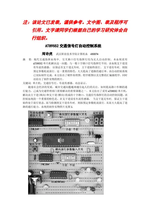
AT89S52交通信号灯自动控制系统周诗虎武汉职业技术学院计算机糸430074摘要: 现代交通指挥糸统中, 交叉路口信号指挥灯均为无人自动控制。
本糸统采用AT89S52单片机解决这一问题。
与一般十字路口信号指挥灯不同,该糸统支干道设有车流传感器,以保证在支干道无车时, 主干道始终放行。
支干道有车时, 则按预定参数轮流放行。
这一重要的特色,大大提高了道路的通行率。
该自动控制系统已实际制作完成。
本文给出了硬件原理图、程序框图以及完整的汇编源程序。
同时还给出了制作实物的照片。
关键词: 单片机,交通信号灯,车流传感器,动态显示。
随着社会经济的发展,城市交通问题越来越引起人们的关注。
如何提高路口车辆的通行能力,己成为交通管理部门需要解决的重要课题之一。
本文给出了采用AT89S52单片机,解决由主干道(纵向)和支干道(横向)组成的十字路口,交通信号指挥灯的自动控制问题。
该控制糸统的一个重要的特色是,在支干道设有车流传感器,当支干道无车时, 保证主干道始终处于放行状态。
而当检测到支干道有车时, 则按预定参数轮流放行。
从而大大提高了道路的通行能力。
糸统的制作实物照片见图1.图1.实物照片一.基本控制系统基本控制系统硬件原理图见图2。
图中IC0为单片机AT89S52,它是美国Atmel 公司的产品。
AT89S52是一种低功耗、高性能CMOS8位微控制器,具有8K 在系统可编程Flash 存储器。
使用Atmel 公司高密度非易失性存储器技术制造,与工业80C51 产品指令和引脚完全兼容。
在单芯片上,拥有灵巧的8 位CPU 和在系统可编程Flash,使得AT89S52为众多嵌入式控制应用系统提供高灵活、超有效的解决方案。
另外它还具有掉电后中断可唤醒、看门狗定时器、三级加密程序存储器等功能。
且8K字节在系统可编程Flash存储器有1000次的擦写周期。

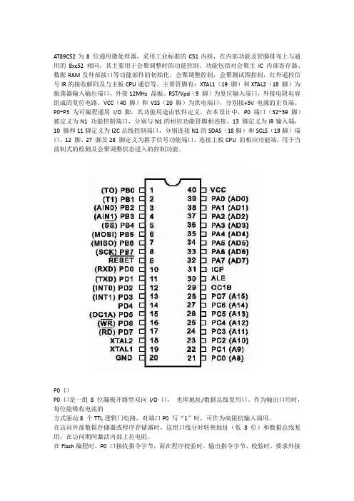
AT89C52为8 位通用微处理器,采用工业标准的C51内核,在内部功能及管脚排布上与通用的8xc52 相同,其主要用于会聚调整时的功能控制。
功能包括对会聚主IC 内部寄存器、数据RAM及外部接口等功能部件的初始化,会聚调整控制,会聚测试图控制,红外遥控信号IR的接收解码及与主板CPU通信等。
主要管脚有:XTAL1(19 脚)和XTAL2(18 脚)为振荡器输入输出端口,外接12MHz 晶振。
RST/Vpd(9 脚)为复位输入端口,外接电阻电容组成的复位电路。
VCC(40 脚)和VSS(20 脚)为供电端口,分别接+5V电源的正负端。
P0~P3 为可编程通用I/O 脚,其功能用途由软件定义,在本设计中,P0 端口(32~39 脚)被定义为N1 功能控制端口,分别与N1的相应功能管脚相连接,13 脚定义为IR输入端,10 脚和11脚定义为I2C总线控制端口,分别连接N1的SDAS(18脚)和SCLS(19脚)端口,12 脚、27 脚及28 脚定义为握手信号功能端口,连接主板CPU 的相应功能端,用于当前制式的检测及会聚调整状态进入的控制功能。
P0 口P0 口是一组8 位漏极开路型双向I/O 口,也即地址/数据总线复用口。
作为输出口用时,每位能吸收电流的方式驱动8 个TTL逻辑门电路,对端口P0 写“1”时,可作为高阻抗输入端用。
在访问外部数据存储器或程序存储器时,这组口线分时转换地址(低8 位)和数据总线复用,在访问期间激活内部上拉电阻。
在Flash编程时,P0 口接收指令字节,而在程序校验时,输出指令字节,校验时,要求外接上拉电阻。
P1 口P1 是一个带内部上拉电阻的8 位双向I/O 口,P1 的输出缓冲级可驱动(吸收或输出电流)4 个TTL 逻辑门电路。
对端口写“1”,通过内部的上拉电阻把端口拉到高电平,此时可作输入口。
作输入口使用时,因为内部存在上拉电阻,某个引脚被外部信号拉低时会输出一个电流(IIL)。
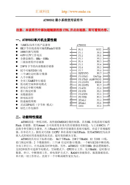
AT89S52最小系统使用说明书注意:本说明书中添加超链接的按CTRL并点击连接,即可看到内容。
一、AT89S52单片机主要性能● 与MCS-51单片机产品兼容● 8K字节在线系统可编程Flash存储器● 1000次擦写周期● 4.0V-5.5V工作电压● 全静态操作:0Hz~33Hz● 三级加密程序存储器● 256*8字节的内部数据存储器● 32个可编程I/O口线● 三个16位定时器/计数器● 八个中断源● 全双工UART串行通道● 低功耗空闲和掉电模式● 掉电后中断可唤醒● 看门狗定时器● 双数据指针● 掉电标识符● 快速编程周期● 灵活ISP编程(字节和模式)● 绿色工作包操作二、功能特性描述AT89S52是一种低功耗、高性能CMOS8位微控制器,具有8K 在线系统可编程Flash 存储器。
使用Atmel 公司高密度非易失性存储器技术制造,与工业80C51 产品指令和引脚完全兼容。
片上Flash允许程序存储器在系统可编程,亦适于常规编程器。
在单芯片上,拥有灵巧的8 位CPU 和在系统可编程Flash,使得AT89S52为众多嵌入式控制应用系统提供高灵活、超有效的解决方案。
AT89S52具有以下标准功能:8k字节Flash,256字节RAM,32 位I/O 口线,看门狗定时器,2 个数据指针,三个16 位定时器/计数器,一个6向量2级中断结构,全双工串行口,片内晶振及时钟电路。
另外,AT89S52 可降至0Hz 静态逻辑操作,支持2种软件可选择节电模式。
空闲模式下,CPU停止工作,允许RAM、定时器/计数器、串口、中断继续工作。
掉电保护方式下,RAM内容被保存,振荡器被冻结,单片机一切工作停止,直到下一个中断或硬件复位为止。
三、板子的功能特点简要说明:一、尺寸:85mmX55mm二、主要芯片:AT89S52单片机、MAX232三、工作电压:直流4~6伏四、单片机标准十针下载接口。
(可使用并口下载线和USB下载线下载)另外支持:双龙下载软件以及Easy 51Pro.exe五、特点:1、具有电源指示。
AT89S52单片机介绍 AT89S52是一种低功耗、高性能CMOS8位微控制器,具有8K 在系统可编程Flash 存储器。
使用Atmel 公司高密度非易失性存储器技术制造,与工业80C51 产品指令和引脚完全兼容。
片上Flash允许程序存储器在系统可编程,亦适于常规编程器。
在单芯片上,拥有灵巧的8 位CPU 和在系统可编程Flash,使得AT89S52为众多嵌入式控制应用系统提供高灵活、超有效的解决方案[7]。
2.1.1 主要性能(1)与MCS-51单片机产品兼容(2)8K字节在系统可编程Flash存储器(3)1000次擦写周期(4)全静态操作:0Hz~33Hz(5)三级加密程序存储器(6)32个可编程I/O口线(7)三个16位定时器/计数器(8)八个中断源(9)全双工UART串行通道(10)低功耗空闲和掉电模式(11)掉电后中断可唤醒(12)看门狗定时器(13)双数据指针(14)掉电标识符2.1.2 引脚功能图2.1 AT89S52引脚图VCC : 电源GND : 地P0 口:P0口是一个8位漏极开路的双向I/O口。
作为输出口,每位能驱动8个TTL逻辑电平。
对P0端口写“1”时,引脚用作高阻抗输入。
当访问外部程序和数据存储器时,P0口也被作为低8位地址/数据复用。
在这种模式下,P0具有内部上拉电阻。
在flash编程时,P0口也用来接收指令字节;在程序校验时,输出指令字节。
程序校验时,需要外部上拉电阻。
P1 口:P1 口是一个具有内部上拉电阻的8 位双向I/O 口,p1 输出缓冲器能驱动4 个TTL 逻辑电平。
对P1 端口写“1”时,内部上拉电阻把端口拉高,此时可以作为输入口使用。
作为输入使用时,被外部拉低的引脚由于内部电阻的原因,将输出电流(IIL)。
此外,P1.0和P1.2分别作定时器/计数器2的外部计数输入(P1.0/T2)和时器/计数器2的触发输入(P1.1/T2EX),具体如下表所示。

Features•Compatible with MCS®-51 Products
•8K Bytes of In-System Programmable (ISP) Flash Memory
–Endurance: 1000 Write/Erase Cycles•4.0V to 5.5V Operating Range
•Fully Static Operation: 0 Hz to 33 MHz
•Three-level Program Memory Lock
•256 x 8-bit Internal RAM
•32 Programmable I/O Lines
•Three 16-bit Timer/Counters
•Eight Interrupt Sources
•Full Duplex UART Serial Channel
•Low-power Idle and Power-down Modes
•Interrupt Recovery from Power-down Mode
•Watchdog Timer
•Dual Data Pointer
•Power-off Flag
•Fast Programming Time
•Flexible ISP Programming (Byte and Page Mode)
•Green (Pb/Halide-free) Packaging Option
1.DescriptionThe AT89S52 is a low-power, high-performance CMOS 8-bit microcontroller with 8K bytes of in-system programmable Flash memory. The device is manufactured using Atmel’s high-density nonvolatile memory technology and is compatible with the indus-try-standard 80C51 instruction set and pinout. The on-chip Flash allows the program memory to be reprogrammed in-system or by a conventional nonvolatile memory pro-grammer. By combining a versatile 8-bit CPU with in-system programmable Flash on a monolithic chip, the Atmel AT89S52 is a powerful microcontroller which provides a highly-flexible and cost-effective solution to many embedded control applications.
The AT89S52 provides the following standard features: 8K bytes of Flash, 256 bytes of RAM, 32 I/O lines, Watchdog timer, two data pointers, three 16-bit timer/counters, a six-vector two-level interrupt architecture, a full duplex serial port, on-chip oscillator, and clock circuitry. In addition, the AT89S52 is designed with static logic for operation down to zero frequency and supports two software selectable power saving modes. The Idle Mode stops the CPU while allowing the RAM, timer/counters, serial port, and interrupt system to continue functioning. The Power-down mode saves the RAM con-tents but freezes the oscillator, disabling all other chip functions until the next interrupt or hardware reset.
8-bit Microcontroller with 8K Bytes In-System Programmable Flash
AT89S52
1919C–MICRO–3/05
¸ÃÎĵµÓÉ Foxit Reader ±à¼-°æȨûÓÐ ·-°æ²»¾¿½ö¹©ÆÀ¹À¡£ 21919C–MICRO–3/05
AT89S52
2.Pin Configurations2.140-lead PDIP
2.244-lead TQFP12345678910111213141516171819204039383736353433323130292827262524232221(T2) P1.0(T2 EX) P1.1P1.2P1.3P1.4(MOSI) P1.5(MISO) P1.6(SCK) P1.7RST(RXD) P3.0(TXD) P3.1(INT0) P3.2(INT1) P3.3(T0) P3.4(T1) P3.5(WR) P3.6(RD) P3.7XTAL2XTAL1GND
VCCP0.0 (AD0)P0.1 (AD1)P0.2 (AD2)P0.3 (AD3)P0.4 (AD4)P0.5 (AD5)P0.6 (AD6)P0.7 (AD7)EA/VPPALE/PROGPSENP2.7 (A15)P2.6 (A14)P2.5 (A13)P2.4 (A12)P2.3 (A11)P2.2 (A10)P2.1 (A9)P2.0 (A8)
1234567891011333231302928272625242344434241403938373635341213141516171819202122(MOSI) P1.5(MISO) P1.6(SCK) P1.7RST(RXD) P3.0NC(TXD) P3.1(INT0) P3.2(INT1) P3.3(T0) P3.4(T1) P3.5
P0.4 (AD4)P0.5 (AD5)P0.6 (AD6)P0.7 (AD7)EA/VPPNCALE/PROGPSENP2.7 (A15)P2.6 (A14)P2.5 (A13)
P1.4P1.3P1.2P1.1 (T2 EX)P1.0 (T2)NCVCCP0.0 (AD0)P0.1 (AD1)P0.2 (AD2)P0.3 (AD3)
(WR) P3.6(RD) P3.7XTAL2XTAL1GNDGND(A8) P2.0(A9) P2.1(A10) P2.2(A11) P2.3(A12) P2.4
2.344-lead PLCC2.442-lead PDIP78910111213141516173938373635343332313029(MOSI) P1.5(MISO) P1.6(SCK) P1.7RST(RXD) P3.0NC(TXD) P3.1(INT0) P3.2(INT1) P3.3(T0) P3.4(T1) P3.5P0.4 (AD4)P0.5 (AD5)P0.6 (AD6)P0.7 (AD7)EA/VPPNCALE/PROGPSENP2.7 (A15)P2.6 (A14)P2.5 (A13)
6543214443424140
1819202122232425262728(WR) P3.6(RD) P3.7XTAL2XTAL1GNDNC(A8) P2.0(A9) P2.1(A10) P2.2(A11) P2.3(A12) P2.4
P1.4 P1.3P1.2P1.1 (T2 EX)P1.0 (T2)NCVCCP0.0 (AD0)P0.1 (AD1)P0.2 (AD2)P0.3 (AD3)
123456789101112131415161718192021424140393837363534333231302928272625242322RST(RXD) P3.0(TXD) P3.1(INT0) P3.2(INT1) P3.3(T0) P3.4(T1) P3.5(WR) P3.6(RD) P3.7XTAL2XTAL1GNDPWRGND(A8) P2.0(A9) P2.1(A10) P2.2(A11) P2.3(A12) P2.4(A13) P2.5(A14) P2.6(A15) P2.7
P1.7 (SCK)P1.6 (MISO)P1.5 (MOSI)P1.4P1.3P1.2P1.1 (T2EX)P1.0 (T2)VDDPWRVDDP0.0 (AD0)P0.1 (AD1)P0.2 (AD2)P0.3 (AD3)P0.4 (AD4)P0.5 (AD5)P0.6 (AD6)P0.7 (AD7)EA/VPPALE/PROGPSEN