TPSMA6.8 THRU TPSMA43A
SURFACE MOUNT AUTOMOTIVE TRANSIENT VOLTAGE SUPPRESSOR
Breakdown Voltage -6.8 to 43.0 Volts Peak Pulse Power - 400 Watts
FEATURES
? Plastic package has Underwriters Laboratory Flammability Classification 94V-0? Ideal for automated placement ? Low profile package ? Built-in strain relief
?Exclusive patented PAR?oxide passivated chip construction
? 400W peak pulse power capability with a 10/1000μs waveform,repetition rate (duty cycle): 0.01%? Excellent clamping capability
? Low incremental surge resistance
? Fast response time: typically less than 1.0ps from 0 Volts to V (BR)min.
? For devices with V (BR)≥10V I D are typically less than 1.0μA at T A =150°C
? Designed for under the hood surface mount applications
? High temperature soldering: 250°C/10 seconds at terminals
MECHANICAL DATA
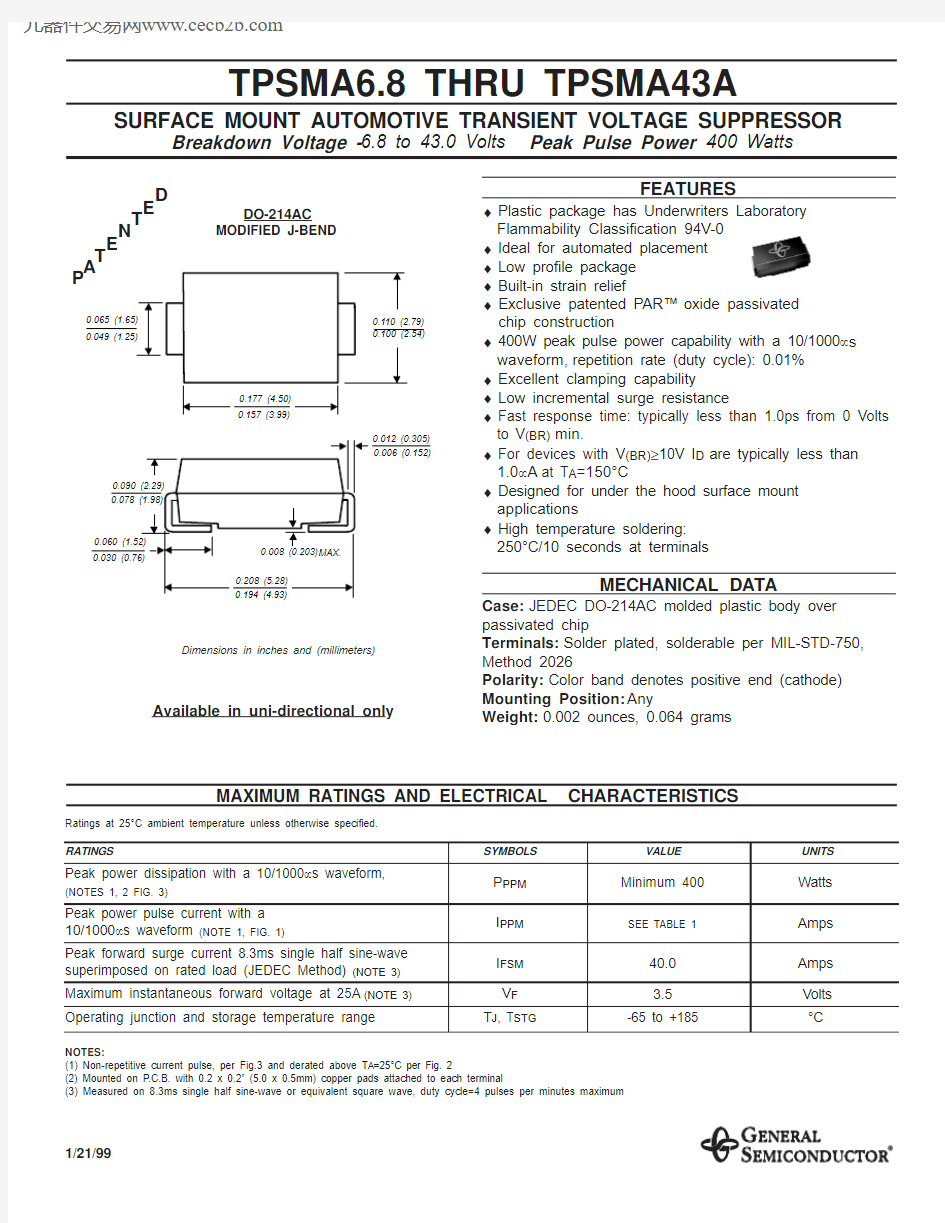
Case:JEDEC DO-214AC molded plastic body over passivated chip
Terminals: Solder plated, solderable per MIL-STD-750,Method 2026
Polarity: Color band denotes positive end (cathode)Mounting Position: Any
Weight: 0.002 ounces, 0.064 grams
MAXIMUM RATINGS AND ELECTRICAL CHARACTERISTICS
Ratings at 25°C ambient temperature unless otherwise specified.
RATINGS SYMBOLS VALUE UNITS
Peak power dissipation with a 10/1000μs waveform,
(NOTES 1, 2 FIG. 3)
P PPM Minimum 400
Watts Peak power pulse current with a 10/1000μs waveform (NOTE 1, FIG. 1)
I PPM SEE TABLE 1
Amps Peak forward surge current 8.3ms single half sine-wave superimposed on rated load (JEDEC Method) (NOTE 3)I FSM 40.0Amps Maximum instantaneous forward voltage at 25A (NOTE 3)V F 3.5Volts Operating junction and storage temperature range
T J , T STG
-65 to +185
°C
NOTES:
(1) Non-repetitive current pulse, per Fig.3 and derated above T A =25°C per Fig. 2
(2) Mounted on P .C.B. with 0.2 x 0.2” (5.0 x 0.5mm) copper pads attached to each terminal
(3) Measured on 8.3ms single half sine-wave or equivalent square wave, duty cycle=4 pulses per minutes maximum
1/21/99
DO-214AC MODIFIED J-BEND
Dimensions in inches and (millimeters)
T E
N
T E
D
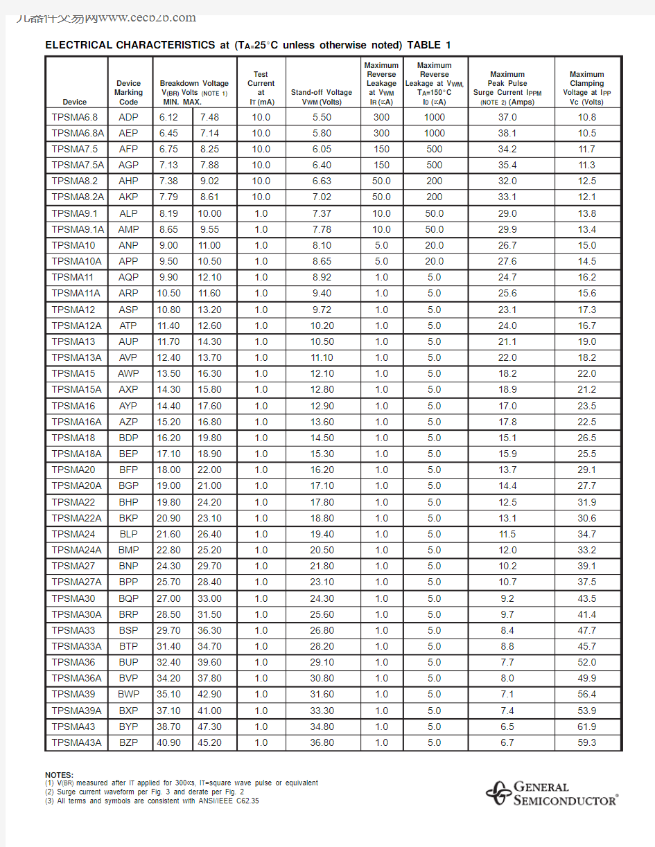
ELECTRICAL CHARACTERISTICS at (T A=25°C unless otherwise noted) TABLE 1
NOTES:
(1) V(BR)measured after I T applied for 300μs, I T=square wave pulse or equivalent
(2) Surge current waveform per Fig. 3 and derate per Fig. 2
(3) All terms and symbols are consistent with ANSI/IEEE C62.35
012
34
100
150
50
0255075100125150175200
25
50
75
100
1.0μs 10μs 100μs 1.0ms 10ms
0.11.0
10
100
0.1μs
FIG. 1 - PEAK PULSE POWER RATING CURVE
P P P M , P E A K P O W E R , k W
td, PULSE WIDTH, sec.
T A , AMBIENT TEMPERATURE, °C
FIG. 3 - PULSE WAVEFORM
t, TIME, ms
I P P M ,P E A K P U L S E C U R R E N T , %
P E A K P U L S E P O W E R (P P P ) o r C U R R E N T (I P P )D E R A T I N G I N P E R C E N T A G E , %
NON-REPETITIVE PULSE WAVEFORM SHOWN IN FIG. 3T A = 25°C
0.2 x 0.2” (5.0 x 5.0mm)COPPER PAD AREAS
PULSE WIDTH (td) is DEFINED as the POINT WHERE the PEAK CURRENT DECAYS to 50% of I PP
tr=10μsec.td
HALF VALUE - I PP
2
10/1000μsec.WAVEFORM as DEFINED by R.E.A.
PEAK VALUE I PPM
FIG. 2 - PULSE DERATING CURVE
125102050100200
10
100
1,000
10,000
1
51050100
1050
100
200
FIG. 4 - TYPICAL JUNCTION CAPACITANCE
V (BR), BREAKDOWN VOLTAGE, VOLTS
NUMBER OF CYCLES AT 60 H Z
C J , J U N C T I O N C A P A C I T A N C E , p F
I F S M ,P E A K F O R W A R D S U R G E C U R R E N T ,A M P E R E S
MEASURED at ZERO BIAS
MEASURED at STAND-OFF VOLTAGE, V WM
8.3ms SINGLE HALF SINE-WAVE (JEDEC Method)T J =T J max
FIG. 5 - MAXIMUM NON-REPETITIVE PEAK FORWARD
SURGE CURRENT
T J =25°C f=1 MHz
Vsig=50mVp-p