外文文献1原文:
DDS devices to produce high-quality waveform: a simple, efficient and flexible
Summary
Direct digital frequency synthesis (DDS) technology for the generation and regulation of high-quality waveforms, widely used in medical, industrial, instrumentation, communications, defense and many other areas. This article will briefly describe the technology, on its strengths and weaknesses, examine some application examples, and also introduced some new products that contribute to the promotion
Introduction
A key requirement in many industries is an exact production, easy operation and quick change of different frequencies, different types of waveforms. Whether it is broadband transceiver requires low phase noise and excellent spurious-free dynamic performance of agile frequency source, or for industrial measurement and control system needs a stable frequency excitation, fast, easy and economical to produce adjustable waveform while maintaining phase continuity capabilities are critical to a design standard, which is what the advantages of direct digital frequency synthesis. Frequency synthesis task
The growing congestion of the spectrum, coupled with lower power consumption, quality of never-ending demand for higher measuring equipment, these factors require the use of the new frequency range, requires a better use of existing frequency range. A result, the search for better control, in most cases, by means of frequency synthesizer for frequency generation. These devices use a given frequency, fC of to generate a target frequency (and phase) fOUT the general relationship can be simply expressed as:
fOUT = εx× fC
Among them, the scale factor εx, sometimes known as the normalized frequency.
The equation is usually gradual approximation of the real number algorithms. When the scale factor is a rational number, two relatively prime numbers (output frequency and reference frequency) than the harmonic. However, in most cases, εx may belong to a broader set of real numbers, the approximation process is within the acceptable range will be truncated
Direct Digital Frequency Synthesizer
The frequency synthesizer a practical way to achieve is the direct digital frequency synthesis (of DDFS), usually referred to as direct digital synthesis (DDS). This technique using digital data processing to generate a frequency and phase adjustable output, the output anda fixed frequency reference clock source fC. related. DDS architecture, the reference or the system clock frequency divided by a scale factor to produce the desired frequency, the scale factor is controlled by the binary tuning word programmable.
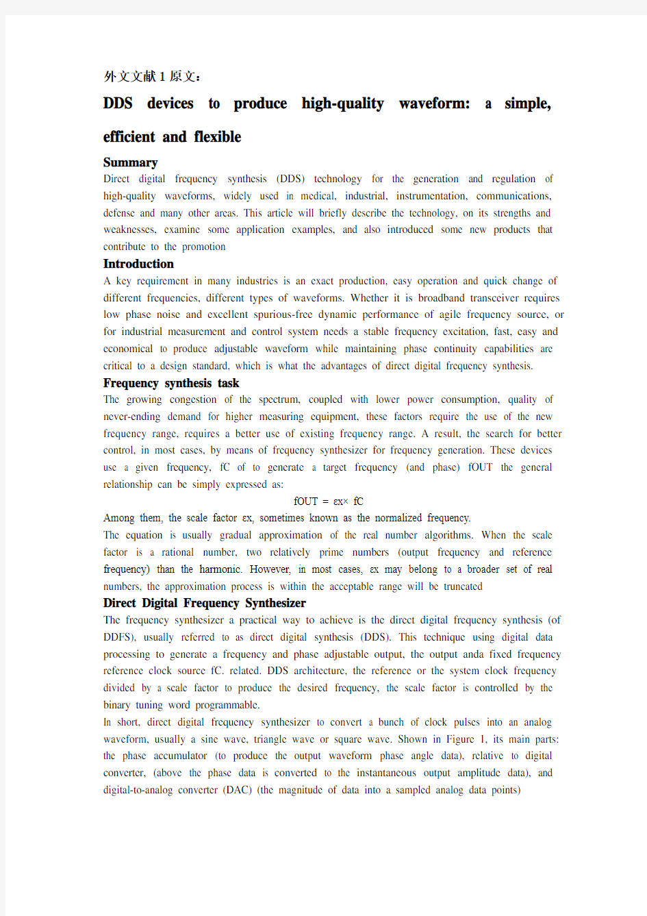
In short, direct digital frequency synthesizer to convert a bunch of clock pulses into an analog waveform, usually a sine wave, triangle wave or square wave. Shown in Figure 1, its main parts: the phase accumulator (to produce the output waveform phase angle data), relative to digital converter, (above the phase data is converted to the instantaneous output amplitude data), and digital-to-analog converter (DAC) (the magnitude of data into a sampled analog data points)
F igure 1.DDS function of the system block diagram.
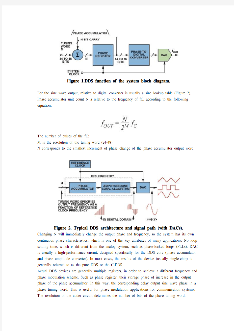
For the sine wave output, relative to digital converter is usually a sine lookup table (Figure 2). Phase accumulator unit count N a relative to the frequency of fC, according to the following equation:
The number of pulses of the fC:
M is the resolution of the tuning word (24-48)
N corresponds to the smallest increment of phase change of the phase accumulator output word
Figure 2. Typical DDS architecture and signal path (with DACs). Changing N will immediately change the output phase and frequency, so the system has its own continuous phase characteristics, which is one of the key attributes of many applications. No loop settling time, which is different from the analog system, such as phase-locked loops (PLLs). DAC is usually a high-performance circuit, designed specifically for the DDS core (phase accumulator and phase amplitude converter). In most cases, the results of the device (usually single-chip) is generally referred to as the pure DDS or the C-DDS.
Actual DDS devices are generally multiple registers, in order to achieve a different frequency and phase modulation scheme. Such as phase register, their storage phase of increase in the output phase of the phase accumulator. In this way, the corresponding delay output sine wave phase in a phase tuning word. This is useful for phase modulation applications for communication systems. The resolution of the adder circuit determines the number of bits of the phase tuning word,
therefore, also decided to delay the resolution.
Integrated in a single device on the engine of a DDS and a DAC has both advantages and disadvantages, however, whether integrated or not, need a DAC to produce ultra-high purity
high-quality analog signal. DAC will convert digital sinusoidal output to an analog sine wave may be single-ended or differential. Some of the key requirements for low phase noise, excellent wideband (WB) and narrowband (NB), spurious-free dynamic range (SFDR), and low power consumption. If the external device, the DAC must be fast enough to handle the signal, so the built-in parallel port device is very common.
DDS and other solutions
The frequency analog phase-locked loops (PLLs), clock generator, and the use of FPGA dynamic programming of the output of the DAC. By examining the spectrum of performance and power of these technologies, a simple comparison, Table 1 shows the qualitative results of the comparison Table 1.DDS with competing technologies - Advanced compare
Power consumption Spectral purity Remarks DDS Low Middle Ease of tuning
Discrete DAC+FPGA Middle Middle-High With tuning capabilities Analog PLL Milddle High Difficult tuning
Phase-locked loop is a feedback loop and its components: a phase comparator, a divider and a pressure-controlled oscillator (VCO), phase comparator reference frequency and output frequency (usually the output frequency is N)frequency) were compared. The error voltage generated by the phase comparator is used to adjust the VCO, thus the output frequency. When the loop is established, the output frequency and / or phase with the reference frequency to maintain a precise relationship. PLL has long been considered in a particular frequency range, high fidelity and consistent signal low phase noise and high spurious free dynamic range (SFDR) are ideal for applications.
PLL can not be precisely and quickly tuning the frequency output waveform, and the slow response, which limits their applicability for fast frequency hopping and part of the frequency shift keying and phase shift keying applications.
Other programs, including integrated DDS engine field programmable gate arrays (FPGAs) - a synthetic sine wave output with the off-the-shelf DAC - though the PLL frequency-hopping problem can be solved, but there own shortcomings. The defects of the major systems work and interface power requirements, high cost, large size, and system developers must also consider the additional software, hardware and memory. For example, using the DDS engine option in the modern FPGA to generate the 10 MHz output signal dynamic range is 60 dB up to 72 kB memory space. In addition, designers need to accept and be familiar with the subtle balance DDS core architecture. .
From a practical point of view (see Table 2), thanks to the rapid development of CMOS technology and modern digital design techniques, as well as the improvement of the DAC topology, DDS technology has been able to achieve unprecedented low power consumption in a wide range of applications, spectrum performance and cost levels. Although the pure DDS products in performance and design flexibility to achieve the level of high-end DAC technology and FPGA, but the advantages of DDS in terms of size, power consumption, cost and simplicity, making it the primary choice for many applications.
Table 2 Benchmark Analysis Summary - frequency generation technique (<50
MHz)
Phase -locked loop DAC + FPGA DDS Spectral performance High High Middle System power requirements High High Middle Digital frequency tuning No Yes Yes Tuning response time High Low Low Solution size Middle High Low Waveform flexibility Low Middle High Cost Middle High Low Design reuse Middle Low High Implementation complexity Middle High Low Also be noted that the DDS device for digital methods to produce the output waveform, it can simplify some of the architecture of the solution, or the waveform of digital programming to create the conditions. Usually with a sine wave to explain the functions and working principle of the DDS, but using modern DDS ICs can easily generate a triangle wave or square wave (clock) output, thereby eliminating the former case the lookup table, and the latter case the DAC the need to integrate a simple and accurate enough.
Performance and limitations of the DDS
Image and envelope: Sin (x) xx roll-off
The actual output of the DAC is not a continuous sine wave, but a series of pulses with a sinusoidal time envelope. The corresponding spectrum is a series of image and signal aliasing. Image along the sin (x) / x envelope distribution (see Figure 3 | margin | graph). The need for the filter to suppress frequencies outside the target band, but can not inhibit the high-level in the passband aliasing (for example, caused due to DAC non-linear)
The Nyquist criterion requires that each cycle requires at least two sampling points in order to rebuild the desired output waveform. The Mirroring response arising from sampling the output frequency K, CLOCK × OUT In this example, which CLOCK = 25 25 MHz and fOUT = 5 MHz, the first and second mirror frequency appear in (see Figure 3) fCLOCK × fOUT, o 20 MHz and 30 MHz. The third and fourth mirror frequency at 45 MHz and 55 MHz. Note, sin (x) / x value of zero at multiples of the sampling frequency. When fOUT greater than the Nyquist bandwidth (1/2 f CLOCK), the first mirror frequency will appear in the Nyquist bandwidth, the occurrence of aliasing (such as 15 MHz signal aliasing down to 10 MHz). Can not use the traditional quist
anti-aliasing filter to filter out aliasing mirror frequency from the output
Sin, in Figure 3.DDS, (x) / x roll-off.
In a typical DDS application, the use of a low-pass filter to suppress the mirror frequency response of the output spectrum. To make the low-pass filter cutoff frequency to remain at reasonable levels, and keep it simple filter design, a feasible approach is the use of an economic low-pass output filter bandwidth limited to about 40% of the frequency of clock.
Any given mirror frequency relative to the amplitude of the fundamental formula of sin (x) / x calculation. Because the function of the frequency roll-off, the basic output of the amplitude and the output frequency is inversely proportional to decrease; in the DDS system, reduce the amount of DC-Nyquist bandwidth range of -3.92 dB.
Significant reduction in frequency in the first mirror - the fundamental 3 dB range. In order to simplify the DDS application filtering, frequency plan must be formulated and analyzed to mirror the frequency and magnitude of the sin (x) / x response in the OUT and CLOCK target frequency spectrum requirements. Other unwanted frequencies in the output spectrum (such as integral and differential linearity error of the DAC, the surge of energy associated with the DAC and clock feed through noise) does not follow the sin (x) / x roll-off response. These unwanted frequencies will be harmonic and spurious energy in the output spectrum in many places - but its magnitude is generally far below the mirror frequency response. DDS devices to the general background noise, substrate noise, thermal noise effects, ground coupling and other signal source coupling factor cumulative portfolio decisions. DDS devices, the noise floor performance of stray and jitter by the circuit board layout, power quality, and - most importantly - Enter the profound impact of the quality of the reference clock.
Shake
The edge of the perfect clock source will be the precise time interval, the interval will never change. Of course, this is not possible; even the best oscillator is also the ideal components constitute, with noise and other defects. Quality and low phase noise crystal oscillator jitter picosecond, and is built up from one million the number of clock edge. The factors leading to jitter external interference, thermal noise, the oscillator circuit instability and power, ground and output connections bring, all these factors will interfere with the timing characteristics of the oscillator. In addition, the oscillator by the external magnetic field or electric field and the nearby transmitter RF interference. Oscillator circuit, a simple amplifier, inverter or buffer to signal additional jitter. Therefore, the choice of a low-jitter, and the edge of steep stable reference clock oscillator is critical. Higher frequency reference clock allows a larger sample, and divide to some extent, reduce the jitter, because the signal to divide a long time to produce the same amount of jitter, which can reduce the jitter on the signal percentage.
Noise - including the phase noise
The sampling system noise depends on many factors, the most important factor is the reference clock jitter, this jitter performance of phase noise on fundamental signal. In the DDS system, the register output of the truncated phase may bring the system error code. The binary word does not lead to the truncation error. But for non-binary word, phase noise truncation error in the spectrum spurious. Spurious frequency / amplitude depends on the code word. Quantification and linearity error of the DAC will be brought to the system harmonic noise. Time-domain error (such as owed to the red / overshoot and code errors) will increase the output signal distortion.
Application
DDS applications can be divided into two categories:
Require agile frequency source for data coding and modulation applications, communications and radar systems
Require measurement of the universal frequency synthesizer features and programmable tuning, scanning, and motivational skills, industrial and optical applications
Both cases, the trend toward higher spectral purity (low phase noise and higher spurious free dynamic range), also low power and small size requirements to accommodate the remote ordemand for battery-powered devices.
Modulation / data encoding, and synchronization of the DDS
DDS products first appeared on the radar and military applications and the development of some of its characteristics (performance improvements, cost and size, etc.) DDS technology is becoming more prevalent in the modulation and data encoding applications. This section will discuss the two data encoding scheme in the DDS system.
Binary frequency shift keying(BFSK, or referred to as FSK) one of the most simple form of data encoding.
The launch of the data is a continuous carrier frequency in two discrete frequency (binary one, ie, pass number, a binary 0, namely, the transformation between the space). Figure 4 shows the relationship between the data and transmit signals.
Figure 4 binary FSK modulation.
Binary 1 and 0 for two different frequencies f0 and f1, respectively. This encoding scheme can be easily DDS device. On behalf of the output frequency of the DDS frequency tuning word change to f0 and f1, will launch the 1 and 0. To transform the output frequency shall dedicated pin FSELECT, containing the appropriate tuning word registers (see Figure 5)
Figure 5. AD9834 or AD9838 DDS tuning word selector realization of the FSK
encoding.
Phase shift keying (PSK) is a simple form of data encoding. In PSK, the carrier frequency
remains the same, by changing the phase of the transmitted signal to transmit information. Can take advantage of a variety of programs to achieve PSK,. The easiest way is often referred to as binary PSK (BPSK), using only two signal phase: 0 ° (logic 1) and 180 ° (logic 0). Members state depends on the status of the former one. If the wave phase remains unchanged, the signal state will remain the same (low or high). Wave phase change 180 °, ie, phase inversion, the signal state will change (low into high or high to low). PSK coding in DDS products can be easily achieved, because most devices have a separate input register (phase register), and phase values can be loaded. This value is added directly to the carrier phase, without changing its frequency. Change the contents of the register will be modulated carrier phase, resulting in a PSK output. For applications that require high-speed modulation, built-in phase register of the AD9834 and
AD9838 allow PSELECT pin signal transformation, according to need modulated carrier in the preloaded phase registers.
The more complex the PSK four or eight-wave phase. Thus, whenever the phase change of binary data transfer rate will be higher than the BPSK modulation. In the four-phase modulation (Quadrature PSK), in the phase angle of 0 ° to +90 °, -90 ° and +180 °; each phase to transform the two signals may represent a factor AD9830, AD9831, AD9832, and the AD9835 provides four phase registers, can be continuously updated register of different phase shift, the complex phase modulation scheme.
The use of synchronous mode of multiple DDS devices to achieve the I / Q Multiple DDS components to achieve the many applications of the I / Q sine wave or square wave signal of known phase relationship between two or more synchronous mode. A common example is the same phase and quadrature modulation (I / Q) in this technique, the phase angle of 0 ° and 90 ° from the carrier frequency signal information. To run two separate DDS components, you can use the same source clock to output can directly control and manipulate the signal of the phase relationship. In Figure 6, with a reference clock on the AD9838 device programming; the RESET pin is used to update the two devices. In this way, you can achieve a simple I / Q modulation RESET after power and initialized before any data to the DDS transmission. DDS output results can be placed in a known phase, making it a common reference point of view, in order to synchronize multiple DDS devices. When new data is sent to multiple DDS devices, the DDS can remain relevant phase relationship, or by the phase offset register can predict the relative phase shift between the adjustments of multiple DDS. The AD983x series of DDS products have a 12 phase resolution, the effective resolution of 0.1 °.
Figure 6. Synchronize the two DDS components.
Author: Brendan Cronin[brendan.cronin @ https://www.doczj.com/doc/9e16367309.html,]ADI core products and
technologies (CPT), a product marketing engineer. Brendan joined the ADI, in 1998 and worked for six years in the industrial and automotive products sector, as mixed-signal design engineers. Brendan is currently the main linear and related technologies.
外文文献1翻译:
DDS器件产生高质量波形:简单、高效而灵活
摘要
直接数字频率合成(DDS)技术用于产生和调节高质量波形,广泛用于医学、工业、仪器仪表、通信、国防等众多领域。本文将简要介绍该技术,说明其优势和不足,考察一些应用示例,同时介绍一些有助于该技术推广的新产品。
简介
许多行业中一个关键的需求是精确产生、轻松操作并快速更改不同频率、不同类型的波形。无论是宽带收发器要求具有低相位噪声和出色的无杂散动态性能的捷变频率源,还是工业测量和控制系统需要稳定的频率激励,快速、轻松、经济地产生可调波形并同时维持相位连续性的能力都是至关重要的一项设计标准,而这正是直接数字频率合成技术的优势所在。频率合成的任务。
不断增多的频谱拥堵,加上对功耗更低、质量更高的测量设备的永无止境的需求,这些因素都要求使用新的频率范围,要求更好地利用现有频率范围。结果,人们寻求对频率产生进行更好的控制,多数情况下,均是借助于频率合成器. 这些器件利用一个给定频率,fC来产生一个相关的目标频率(和相位)fOUT. 其一般关系可以简单地表示为:
fOUT = εx× fC
其中,比例因子εx, 有时也被称为归一化频率.
该等式通常利用实数逐步逼近的算法实现。当比例因子为有理数时,两个相对质数(输出频率和基准频率)之比将谐波相关。但在多数情况下,εx可能属于更广泛的实数集,逼近过程一旦处于可接受的范围之内即会被截断。
直接数字频率合成
频率合成器的一种实用型实现方式是直接数字频率合成 (DDFS), 通常简称为直接数字合成 (DDS). 这种技术利用数字数据处理来产生一个频率和相位可调的输出,该输出与一个固定的频率参考或时钟源fC.相关。在DDS架构中,参考或系统时钟频率由一个比例因子分频来产生所需频率,该比例因子由二进制调谐字可编程控制。
简言之,直接数字频率合成器将一串时钟脉冲转换成一个模拟波形,通常为一个正弦波、三角波或方波。如图1所示,其主要部分为:相位累加器(产生输出波形相位角度的数据),相数转换器,(将上述相位数据转换为瞬时输出幅度数据),以及数模转换器(DAC)(将该幅度数据转换成采样模拟数据点)。
图1.DDS系统的功能框图
对于正弦波输出,相数转换器通常为一个正弦查找表(图2)。相位累加器以N为单位计数,并根据以下等式产生一个相对于fC的频率:
其中:
M为调谐字的分辨率(24至48位)
N为对应于相位累加器输出字最小增量相位变化的fC的脉冲数
图2.典型的DDS架构和信号路径(带DAC)
由于更改N会立即改变输出相位和频率,因此,系统自身具有相位连续,特点,这是许多应用的关键属性之一。无需环路建立时间,这与模拟系统不同,如锁相环(PLL)。DAC通常为一个高性能电路,专门针对DDS内核(相位累加器和相幅转换器)而设计。多数情况下,这样结果形成的器件(通常为单芯片)一般称为纯DDS或C-DDS。
实际的DDS器件一般集成多个寄存器,以实现不同的频率和相位调制方案。如相位寄存器,其存储的相位内容被加在相位累加器的输出相位上。这样,可以对应于一个相位调谐字延迟输出正弦波的相位。对于通信系统相位调制应用,这非常有用。加法器电路的分辨率决定着相位调谐字的位数,因此,也决定着延迟的分辨率。
在单个器件上集成一个DDS引擎和一个DAC既有优点也有缺点,但是,无论集成与否,都需要一个DAC来产生纯度超高的高品质模拟信号。DAC将数字正弦输出转换为一个模拟正弦波,可能是单端,也可能是差分。一些关键要求是低相位噪声、优秀的宽带(WB)和窄带(NB)无杂散动态范围(SFDR)以及低功耗。如果是外部器件,则DAC必须足够快以处理信号,因此,内置并行端口的器件非常常见。
DDS与其他解决方案
其他产生频率的方法包括模拟锁相环(PLL),时钟发生器和利用FPGA对DAC的输出进行动态编程。通过考察频谱性能和功耗,可以对这些技术进行简单的比较,表1以定性方式展示了比较结果。
表1.DDS与竞争技术——高级比较
功耗频谱纯度备注
DDS 低中易于调谐
分立式DAC + FPGA 中中-高具有调谐能力
模拟PLL 中高难以调谐
锁相环是一种反馈环路,其组成部分为:一个相位比较器, 一个除法器和一个压控制振荡器(VCO). 相位比较器将基准频率与输出频率(通常是输出频率的N)分频)进行比较。相位比较器产生的误差电压用于调节VCO,从而输出频率。当环路建立后,输出将在频率和/或相位上与参考频率保持一种精确的关系。PLL长期以来一直被认为是在特定频带范围内要求高保真度和稳定信号的低相位噪声和高无杂散动态范围(SFDR) 应用的理想选择。
由于PLL无法精确、快速地调谐频率输出和波形,而且响应较慢,这限制了它们对于快速跳频和部分频移键控和相移键控应用的适用性。
其他方案,包括集成DDS引擎的现场可编程门阵列(FPGAs) ——配合现成DAC以合成输出正弦波——虽然可以解决PLL的跳频问题,但也存在自身的缺陷。主要系统缺陷包括较高的工作和接口功耗要求、成本较高、尺寸较大,而且系统开发人员还须考虑额外的软件、硬件和存储器问题。例如,利用现代FPGA中的DDS引擎选项,要产生动态范围为60 dB的10 MHz输出信号,需要多达72 kB的存储器空间。另外,设计师需要接受并熟悉细微权衡和DDS内核的架构。
从实用角度来看(见表2),得益于CMOS工艺和现代数字设计技术的快速发展以及DAC 拓扑结构的改进,DDS技术已经能在广泛的应用中实现前所未有的低功耗、频谱性能和成本水平。虽然纯DDS产品不可能在性能和设计灵活性上达到高端DAC技术与FPGA相结合的水平,但DDS在尺寸、功耗、成本和简单性方面的优势使其成为许多应用的首要选择。
表2.基准分析小结——频率产生技术(<50 MHz)
锁相环DAC + FPGA DD S
频谱性能高高中
系统功耗要求高高低
数字频率调谐无是是
调谐响应时间高低低
解决方案尺寸中高低
波形灵活性低中高
成本中高低
设计重用中低高
实现复杂度中高低
同时需要指出,由于DDS器件从根本上来说是用数字方法产生输出波形,因此它可以简化一些解决方案的架构,或者为对波形进行数字化编程创造条件。尽管通常利用正弦波来解释DDS的功能和工作原理,但利用现代DDS IC也可以轻松产生三角波或方波(时钟)输出,由此消除了前一种情况的查找表以及后一种情况的DAC的必要性,因为集成一个简单而精确的比较器就够了。
DDS的性能与限制
图像和包络:Sin(x)xx滚降
DAC的实际输出不是连续的正弦波,而是带有正弦时间包络的一系列脉冲。对应的频谱是一系列图像和混叠信号。图像沿sin(x)/x 包络分布(见图3中的|幅度|曲线图)。有必要进行滤波,以抑制目标频带之外的频率,但是不能抑制通带中出现的高阶混叠(例如,因DAC 非线性所致)。
奈奎斯特准则要求,每个周期至少需要两个采样点才能重建所需输出波形。镜像响应产生于采样输出频率中K fCLOCK ×fOUT. 在本例中,其中fCLOCK = 25 25 MHz且fOUT = 5 MHz,第一和第二镜频出现在(见图3)fCLOCK ×fOUT, o即20 MHz和30 MHz。第三和第四镜频出现在45 MHz和55 MHz。注意,sin(x)/x零值出现在采样频率的倍数处。当fOUT 大于奈奎斯特带宽(1/2 fCLOCK), 时,第一镜频将出现于奈奎斯特带宽之内,发生混叠(例如,15 MHz的信号将向下混叠至10 MHz)。无法用传统的奈奎斯特抗混叠滤波器从输出中滤掉混叠镜频。
图3.DDS中的Sin(x)/x滚降
在典型的DDS应用中,利用一个低通滤波器来抑制输出频谱中镜频响应的影响。为了使低通滤波器的截止频率要求保持于合理水平,并使滤波器设计保持简单,一种可行的做法是利用一个经济的低通输出滤波器将fOUT 带宽限制在fCLOCK频率的40%左右。
任何给定镜频相对于基波的幅度可用sin(x)/x公式来计算。由于该函数随频率滚降,因此基本输出的幅度将与输出频率成反比而降低;在DDS系统中,降低量为DC-奈奎斯特带宽范围的–3.92 dB。
第一镜频的幅度较大——基波的3 dB范围内。为了简化DDS应用的滤波要求,必须制定频率计划,并分析镜频和sin(x)/x幅度响应在fOUT和fCLOCK目标频率下的频谱要求。输出频谱中的其他不需要的频率(如DAC的积分和微分线性误差、与DAC相关的突波能量和时钟馈通噪声)不会遵循sin(x)/x滚降响应。这些不需要的频率将以谐波和杂散能量出现在输出频谱中的许多地方——但其幅度一般会远远低于镜频响应。DDS器件的一般本底噪声由基板噪声、热噪声效应、接地耦合和其他信号源耦合等因素累积组合决定。DDS器件的本底噪声、性能杂散和抖动受到电路板布局、电源质量以及——最重要的是——输入参考时钟。
抖动
完美时钟源的边沿将以精确的时间间隔发生,而该间隔永远都不会变化。当然,这是不可能的;即使最好的振荡器也是由不理想的元件构成,具有噪声等缺陷。优质的低相位噪声晶体振荡器的抖动为皮秒级,而且是从数百万个时钟边沿累积起来的。导致抖动的因素有热噪声、振荡器电路不稳定以及电源、接地和输出连接等带来的外部干扰等,所有这些因素都
会干扰振荡器的时序特性。另外,振荡器受外部磁场或电场以及附近发射器的射频干扰的影响。振荡器电路中,一个简单的放大器、反相器或缓冲器也都会给信号带来额外的抖动。
因此,选择一个抖动低、边沿陡的稳定的参考时钟振荡器是至关重要的。较高频率的基准时钟允许较大的过采样,而且,通过分频可以在一定程度上减轻抖动,因为对信号进行分频将在更长时期产生相同量的抖动,因而可以降低信号上的抖动的百分比。
质量的深刻影响。
噪声——包括相位噪声
采样系统的噪声取决于诸多因素,首要因素是参考时钟抖动,这种抖动表现为基波信号上的相位噪声。在DDS系统中,截断相位寄存器输出可能带来因代码而异的系统误差。二进制字不会导致截断误差。但对于非二进制字,相位噪声截断误差会在频谱中产生杂散。杂散的频率/幅度取决于代码字。DAC的量化和线性误差也会给系统带来谐波噪声。时域误差(如欠冲/过冲和代码错误)都会加重输出信号的失真。
应用
DDS应用可以分为两大类:
1、要求捷变频率源以进行数据编码和调制应用的通信和雷达系统
2、要求通用频率合成功能以及可编程调谐、扫描和激励能力的测量、工业和光学应用
两种情况下,都出现了一种走向更高频谱纯度(更低的相位噪声和更高的无杂散动态范围)的趋势,同时还存在低功耗和小尺寸的要求,以适应远程或电池供电设备的需求。
调制/数据编码和同步中的DDS
DDS产品首先出现于雷达和军事应用之中,其部分特性的发展(性能的提升、成本和尺寸等)已使DDS技术在调制和数据编码应用中日渐盛行。本节将讨论两种数据编码方案及其在DDS系统中的实现方式。
二进制频移键控 (BFSK,或简称FSK) 最简单的数据编码形式之一
数据的发射方式是使一个连续载波的频率在两个离散频率(一为二进制1,即传号,一为二进制0,即空号)之间变换。图4所示为数据和发射信号之间的关系。
图4.二进制FSK调制
二进制1和0表示为两个不同的频率,分别为f0和f1。这种编码方案可以轻松在DDS器件中实现。代表输出频率的DDS频率调谐字被改变,以从将发射的1和0产生f0和f1。要变换输出频率,则须用专用的引脚FSELECT选择含有相应调谐字的寄存器(见图5)。
图5.利用AD9834或AD9838 DDS的调谐字选择器实现FSK编码
相移键控(PSK) 是另一种简单的数据编码形式。在PSK中,载波的频率保持不变,通过改变发射信号的相位来传递信息。可以利用多种方案来实现PSK。最简单的方法通常称为二进制PSK(即BPSK),只采用两个信号相位:0°(逻辑1)和180°(逻辑0)。各位的状态取决于前一位的状态。如果波的相位不变,则信号状态将保持不变(低或高)。如果波的相位改变180°,即相位反转,则信号状态将改变(低变为高,或高变为低)。PSK编码可以轻松在DDS产品中实现,因为多数器件都有一个独立的输入寄存器(相位寄存器),可以加载相位值。该值被直接添加到载波的相位,而不改变其频率。更改该寄存器的内容将调制载波的相位,结果产生一个PSK输出。对于要求高速调制的应用,内置相位寄存器对的AD9834和AD9838允许其PSELECT引脚上的信号在预加载的相位寄存器之间变换,以根据需要调制载波。
更复杂的PSK采用四个或八个波相位。这样,每当相位发生变化时,二进制数据的传输速率将高于BPSK调制。在四相位调制(正交PSK),中,可能的相位角度为0°, +90°, ?90°, 和+180°;每次相位变换可能代表两个信号因子AD9830, AD9831, AD9832, 和AD9835 提供四个相位寄存器,通过连续更新寄存器的不同相位偏移,可以实现复杂的相位调制方案.。
以同步模式利用多个DDS元件实现I/Q功能
许多应用要求产生两个或两个以上具有已知相位关系的正弦波或方波信号。一个常见的例子是同相和正交调制(I/Q),在这种技术中,在0°和90°相位角度从载波频率获得信号信息。可以用相同的源时钟来运行两个单独的DDS元件,以输出可以直接控制和操作其相位关系的信号。在图6中,用一个基准时钟对AD9838器件编程;相同的RESET引脚用于更新两个器件。这样,可以实现简单的I/Q调制。
RESET必须在上电后以及向DDS传输任何数据之前初始化。结果可将DDS输出置于已知相位,使其成为共同的参考角度,以便同步多个DDS器件。当新数据被同时送至多个DDS 器件时,DDS之间可以保持相关相位关系,或者通过相位偏移寄存器可以预测性调整多个DDS之间的相对相位偏移。AD983x系列DDS产品拥有12位相位分辨率,有效分辨率为0.1°。
图6.同步两个DDS元件
作者:Brendan Cronin[brendan.cronin@https://www.doczj.com/doc/9e16367309.html,]是ADI核心产品和技术(CPT)
部门的一位产品营销工程师。Brendan于1998年加盟ADI,在工业和汽车产品部门工作了六年,担任混合信号设计工程师。Brendan目前主要研究线性和相关技术。
外文文献原文2:
Ask The Application Engineer—33
All About Direct Digital Synthesis
By Eva Murphy, (eva.murphy@https://www.doczj.com/doc/9e16367309.html,)
Colm Slattery (colm.slattery@https://www.doczj.com/doc/9e16367309.html,)
By Analog Dialogue V olume 38 Number 3 of ADI
What is Direct Digital Synthesis?
Direct digital synthesis (DDS) is a method of producing an analog waveform—usually a sine wave—by generating a time-varying signal in digital form and then performing a digital-to-analog conversion. Because operations within a DDS device are primarily digital, it can offer fast switching between output frequencies, fine frequency resolution, and operation over a broad spectrum of frequencies. With advances in design and process technology, today’s DDS devices are very compact and draw little power.
Why would one use a direct digital synthesizer (DDS)? Aren’t there other methods for easily generating frequencies?
The ability to accurately produce and control waveforms of various frequencies and profiles has become a key requirement common to a number of industries. Whether providing agile sources of low-phase-noise variable-frequencies with good spurious performance for communications, or simply generating a frequency stimulus in industrial or biomedical test equipment applications,
convenience, compactness, and low cost are important design considerations.
Many possibilities for frequency generation are open to a designer, ranging from
phase-locked-loop (PLL)-based techniques for very high-frequency synthesis, to dynamic programming of digital-to-analog converter (DAC) outputs to generate arbitrary waveforms at lower frequencies. But the DDS technique is rapidly gaining acceptance for solving frequency- (or waveform) generation requirements in both communications and industrial applications because single-chip IC devices can generate programmable analog output waveforms simply and with high resolution and accuracy.
Furthermore, the continual improvements in both process technology and design have resulted in cost and power consumption levels that were previously unthinkably low. For example, the
AD9833, a DDS-based programmable waveform generator (Figure 1), operating at 5.5 V with a 25-MHz clock, consumes a maximum power of 30 milliwatts.
Figure 1. The AD9833—a one-chip waveform generator.
What are the main benefits of using a DDS?
DDS devices like the AD9833 are programmed through a high speed serial peripheral-interface (SPI), and need only an external clock to generate simple sine waves. DDS devices are now available that can generate frequencies from less than 1 Hz up to 400 MHz (based on a 1-GHz clock). The benefits of their low power, low cost, and single small package, combined with their inherent excellent performance and the ability to digitally program (and reprogram) the output waveform, make DDS devices an extremely attractive solution—preferable to less-flexible solutions comprising aggregations of discrete elements.
What kind of outputs can I generate with a typical DDS device?
DDS devices are not limited to purely sinusoidal outputs. Figure 2 shows the square-, triangular-, and sinusoidal outputs available from an AD9833.
Figure 2. Square-, triangular-, and sinusoidal outputs from a DDS.
How does a DDS device create a sine wave?
Here’s a breakdown of the internal circuitry of a DDS device: its main components are a phase accumulator, a means of phase-to-amplitude conversion (often a sine look-up table), and a DAC. These blocks are represented in Figure 3.
Figure 3. Components of a direct digital synthesizer.
A DDS produces a sine wave at a given frequency. The frequency depends on two variables, the reference-clock frequency and the binary number programmed into the frequency register (tuning word).
The binary number in the frequency register provides the main input to the phase accumulator. If a sine look-up table is used, the phase accumulator computes a phase (angle) address for the look-up table, which outputs the digital value of amplitude—corresponding to the sine of that phase angle—to the DAC. The DAC, in turn, converts that number to a corresponding value of analog voltage or current. To generate a fixed-frequency sine wave, a constant value (the phase increment—which is determined by the binary number) is added to the phase accumulator with each clock cycle. If the phase increment is large, the phase accumulator will step quickly through the sine look-up table and thus generate a high frequency sine wave. If the phase increment is
small, the phase accumulator will take many more steps, accordingly generating a slower waveform.
Let’s talk some more about the phase accumulator. How does it work? Continuous-time sinusoidal signals have a repetitive angular phase range of 0 to 2π. The digital implementation is no different. The counter’s carry function allows the phase accu mulator to act as a phase wheel in the DDS implementation.
To understand this basic function, visualize the sine-wave oscillation as a vector rotating around a phase circle (see Figure 4). Each designated point on the phase wheel corresponds to the equivalent point on a cycle of a sine wave. As the vector rotates around the wheel, visualize that the sine of the angle generates a corresponding output sine wave. One revolution of the vector around the phase wheel, at a constant speed, results in one complete cycle of the output sine wave. The phase accumulator provides the equally spaced angular values accompanying the vector’s linear rotation around the phase wheel. The contents of the phase accumulator correspond to the points on the cycle of the output sine wave.
Figure 4. Digital phase wheel.
The phase accumulator is actually a modulo-M counter that increments its stored number each time it receives a clock pulse. The magnitude of the increment is determined by the binary-coded input word (M). This word forms the phase step size between reference-clock updates; it effectively sets how many points to skip around the phase wheel. The larger the jump size, the faster the phase accumulator overflows and completes its equivalent of a sine-wave cycle. The number of discrete phase points contained in the wheel is determined by the resolution of the phase accumulator (n), which determines the tuning resolution of the DDS. For an n = 28-bit phase accumulator, an M value of 0000...0001 would result in the phase accumulator overflowing after 228 reference-clock cycles (increments). If the M value is changed to 0111...1111, the phase accumulator will overflow after only 2 reference-clock cycles (the minimum required by Nyquist). This relationship is found in the basic tuning equation for DDS architecture:
where:
f OUT = output frequency of the DDS
M = binary tuning word
f C = internal reference clock frequency (system clock)
n = length of the phase accumulator, in bits
Changes to the value of M result in immediate and phase-continuous changes in the output frequency. No loop settling time is incurred as in the case of a phase-locked loop.
As the output frequency is increased, the number of samples per cycle decreases. Since sampling theory dictates that at least two samples per cycle are required to reconstruct the output waveform, the maximum fundamental output frequency of a DDS is f C/2. However, for practical applications, the output frequency is limited to somewhat less than that, improving the quality of the reconstructed waveform and permitting filtering on the output.
When generating a constant frequency, the output of the phase accumulator increases linearly, so the analog waveform it generates is inherently a ramp.
Then how is that linear output translated into a sine wave?
A phase-to-amplitude lookup table is used to convert the phase-a ccumulator’s instantaneous output value (28 bits for AD9833)—with unneeded less-significant bits eliminated by truncation—into the sine-wave amplitude information that is presented to the (10-bit) D/A converter. The DDS architecture exploits the symmetrical nature of a sine wave and utilizes mapping logic to synthesize a complete sine wave from one-quarter-cycle of data from the phase accumulator. The phase-to- amplitude lookup table generates the remaining data by reading forward then back through the lookup table. This is shown pictorially in Figure 5.
Figure 5. Signal flow through the DDS architecture.
What are popular uses for DDS?
Applications currently using DDS-based waveform generation fall into two principal categories: Designers of communications systems requiring agile (i.e., immediately responding) frequency sources with excellent phase noise and low spurious performance often choose DDS for its combination of spectral performance and frequency-tuning resolution. Such applications include using a DDS for modulation, as a reference for a PLL to enhance overall frequency tunability, as a local oscillator (LO), or even for direct RF transmission.
Alternatively, many industrial and biomedical applications use a DDS as a programmable
waveform generator. Because a DDS is digitally programmable, the phase and frequency of a waveform can be easily adjusted without the need to change the external components that would normally need to be changed when using traditional analog-programmed waveform generators. DDS permits simple adjustments of frequency in real time to locate resonant frequencies or compensate for temperature drift. Such applications include using a DDS in adjustable frequency sources to measure impedance (for example in an impedance-based sensor), to generate
pulse-wave modulated signals for micro-actuation, or to examine attenuation in LANs or telephone cables.
What do you consider to be the key advantages of DDS to designers of real-world equipment and systems?
Today’s cost-competitive, high-performance, functionally integrated DDS ICs are becoming common in both communication systems and sensor applications. The advantages that make them attractive to design engineers include:
?digitally controlled micro-hertz frequency-tuning and sub-degree phase-tuning capability, ?extremely fast hopping speed in tuning output frequency (or phase); phase-continuous frequency hops with no overshoot/undershoot or analog-related loop settling-time anomalies, ?the digital architecture of DDS eliminates the need for the manual tuning and tweaking related to component aging and temperature drift in analog synthesizer solutions, and
?the digital control interface of the DDS architecture facilitates an environment where systems can be remotely controlled and optimized with high resolution under processor
control.
How would I use a DDS device for FSK encoding?
Binary frequency-shift keying (usually referred to simply as FSK) is one of the simplest forms of data encoding. The data is transmitted by shifting the frequency of a continuous carrier to one of two discrete frequencies (hence binary). One frequency, f1, (perhaps the higher) is designated as the mark frequency (binary one) and the other, f0, as the space frequency (binary zero). Figure 6 shows an example of the relationship between the mark-space data and the transmitted signal.
Figure 6. FSK modulation.
This encoding scheme is easily implemented using a DDS. The DDS frequency tuning word, representing the output frequencies, is set to the appropriate values to generate f0 and f1 as they occur in the pattern of 0s and 1s to be transmitted. The user programs the two required tuning words into the device before transmission. In the case of the AD9834, two frequency registers are available to facilitate convenient FSK encoding. A dedicated pin on the device (FSELECT) accepts the modulating signal and selects the appropriate tuning word (or frequency register). The
block diagram in Figure 7 demonstrates a simple implementation of FSK encoding.
Figure 7. A DDS-based FSK encoder.
And how about PSK coding?
Phase-shift keying (PSK) is another simple form of data encoding. In PSK, the frequency of the carrier remains constant and the phase of the transmitted signal is varied to convey the information.
Of the schemes to accomplish PSK, the simplest-known as binary PSK (BPSK)—uses just two signal phases: 0 degrees and 180 degrees. BPSK encodes 0° phase shift for a logic 1 input and 180° phase shift for a logic 0 input. The state of each bit is determined according to the state of the preceding bit. If the phase of the wave does not change, the signal state stays the same (low or high). If the phase of the wave reverses (changes by 180 degrees), then the signal state changes (from low to high, or from high to low).
PSK encoding is easily implemented with DDS ICs. Most of the devices have a separate input register (a phase register) that can be loaded with a phase value. This value is directly added to the phase of the carrier without changing its frequency. Changing the contents of this register modulates the phase of the carrier, thus generating a PSK output signal. For applications that require high speed modulation, the AD9834 allows the preloaded phase registers to be selected using a dedicated toggling input pin (PSELECT), which alternates between the registers and modulates the carrier as required.
More sophisticated forms of PSK employ four- or eight- wave phases. This allows binary data to be transmitted at a faster rate per phase change than is possible with BPSK modulation. In
four-phase modulation (quadrature PSK or QPSK), the possible phase angles are 0, +90, –90, and 180 degrees; each phase shift can represent two signal elements. The AD9830, AD9831, AD9832, and AD9835 provide four phase registers to allow complex phase modulation schemes to be implemented by continuously updating different phase offsets to the registers.
Can multiple DDS devices be synchronized for, say, I-Q capability?
It is possible to use two single DDS devices that operate on the same master clock to output two signals whose phase relationship can then be directly controlled. In Figure 8, two AD9834s are programmed using one reference clock, with the same reset pin being used to update both parts. Using this setup, it is possible to do I-Q modulation.
中英文对照外文翻译 (文档含英文原文和中文翻译) Create and comprehensive technology in the structure global design of the building The 21st century will be the era that many kinds of disciplines technology coexists , it will form the enormous motive force of promoting the development of building , the building is more and more important too in global design, the architect must seize the opportunity , give full play to the architect's leading role, preside over every building engineering design well. Building there is the global design concept not new of architectural design,characteristic of it for in an all-round way each element not correlated with building- there aren't external environment condition, building , technical equipment,etc. work in coordination with, and create the premium building with the comprehensive new technology to combine together. The premium building is created, must consider sustainable development , namely future requirement , in other words, how save natural resources as much as possible, how about protect the environment that the mankind depends on for existence, how construct through high-quality between architectural design and building, in order to reduce building equipment use quantity and
机械设计 摘要:机器是由机械装置和其它组件组成的。它是一种用来转换或传递能量的装置,例如:发动机、涡轮机、车辆、起重机、印刷机、洗衣机、照相机和摄影机等。许多原则和设计方法不但适用于机器的设计,也适用于非机器的设计。术语中的“机械装置设计”的含义要比“机械设计”的含义更为广泛一些,机械装置设计包括机械设计。在分析运动及设计结构时,要把产品外型以及以后的保养也要考虑在机械设计中。在机械工程领域中,以及其它工程领域中,所有这些都需要机械设备,比如:开关、凸轮、阀门、船舶以及搅拌机等。 关键词:设计流程设计规则机械设计 设计流程 设计开始之前就要想到机器的实际性,现存的机器需要在耐用性、效率、重量、速度,或者成本上得到改善。新的机器必需具有以前机器所能执行的功能。 在设计的初始阶段,应该允许设计人员充分发挥创造性,不要受到任何约束。即使产生了许多不切实际的想法,也会在设计的早期,即在绘制图纸之前被改正掉。只有这样,才不致于阻断创新的思路。通常,还要提出几套设计方案,然后加以比较。很有可能在这个计划最后决定中,使用了某些不在计划之内的一些设想。 一般的当外型特点和组件部分的尺寸特点分析得透彻时,就可以全面的设计和分析。接着还要客观的分析机器性能的优越性,以及它的安全、重量、耐用性,并且竞争力的成本也要考虑在分析结果之内。每一个至关重要的部分要优化它的比例和尺寸,同时也要保持与其它组成部分相协调。 也要选择原材料和处理原材料的方法。通过力学原理来分析和实现这些重要的特性,如那些静态反应的能量和摩擦力的最佳利用,像动力惯性、加速动力和能量;包括弹性材料的强度、应力和刚度等材料的物理特性,以及流体润滑和驱动器的流体力学。设计的过程是重复和合作的过程,无论是正式或非正式的进行,对设计者来说每个阶段都很重要。 最后,以图样为设计的标准,并建立将来的模型。如果它的测试是符合事先要
英文原文出自《Advanced Technology Libraries》2008年第5期 Robot Robot is a type of mechantronics equipment which synthesizes the last research achievement of engine and precision engine, micro-electronics and computer, automation control and drive, sensor and message dispose and artificial intelligence and so on. With the development of economic and the demand for automation control, robot technology is developed quickly and all types of the robots products are come into being. The practicality use of robot products not only solves the problems which are difficult to operate for human being, but also advances the industrial automation program. At present, the research and development of robot involves several kinds of technology and the robot system configuration is so complex that the cost at large is high which to a certain extent limit the robot abroad use. To development economic practicality and high reliability robot system will be value to robot social application and economy development. With the rapid progress with the control economy and expanding of the modern cities, the let of sewage is increasing quickly: With the development of modern technology and the enhancement of consciousness about environment reserve, more and more people realized the importance and urgent of sewage disposal. Active bacteria method is an effective technique for sewage disposal,The lacunaris plastic is an effective basement for active bacteria adhesion for sewage disposal. The abundance requirement for lacunaris plastic makes it is a consequent for the plastic producing with automation and high productivity. Therefore, it is very necessary to design a manipulator that can automatically fulfill the plastic holding. With the analysis of the problems in the design of the plastic holding manipulator and synthesizing the robot research and development condition in recent years, a economic scheme is concluded on the basis of the analysis of mechanical configuration, transform system, drive device and control system and guided by the idea of the characteristic and complex of mechanical configuration,
forced concrete structure reinforced with an overviewRein Since the reform and opening up, with the national economy's rapid and sustained development of a reinforced concrete structure built, reinforced with the development of technology has been great. Therefore, to promote the use of advanced technology reinforced connecting to improve project quality and speed up the pace of construction, improve labor productivity, reduce costs, and is of great significance. Reinforced steel bars connecting technologies can be divided into two broad categories linking welding machinery and steel. There are six types of welding steel welding methods, and some apply to the prefabricated plant, and some apply to the construction site, some of both apply. There are three types of machinery commonly used reinforcement linking method primarily applicable to the construction site. Ways has its own characteristics and different application, and in the continuous development and improvement. In actual production, should be based on specific conditions of work, working environment and technical requirements, the choice of suitable methods to achieve the best overall efficiency. 1、steel mechanical link 1.1 radial squeeze link Will be a steel sleeve in two sets to the highly-reinforced Department with superhigh pressure hydraulic equipment (squeeze tongs) along steel sleeve radial squeeze steel casing, in squeezing out tongs squeeze pressure role of a steel sleeve plasticity deformation closely integrated with reinforced through reinforced steel sleeve and Wang Liang's Position will be two solid steel bars linked Characteristic: Connect intensity to be high, performance reliable, can bear high stress draw and pigeonhole the load and tired load repeatedly.
The future of the tall building and structure of buildings Zoning effects on the density of tall buildings and solar design may raise ethical challenge. A combined project of old and new buildings may bring back human scale to our cities. Owners and conceptual designers will be challenged in the 1980s to produce economically sound, people-oriented buildings. In 1980 the Level House, designed by Skidmore, Owings and Merril1 (SOM) received the 25-year award from the American Institute of Architects “in recogn ition of architectural design of enduring significance”. This award is given once a year for a building between 25and 35 years old .Lewis Mumford described the Lever House as “the first office building in which modern materials, modern construction, modern functions have been combined with a modern plan”. At the time, this daring concept could only be achieved by visionary men like Gordon Bunshaft, the designer , and Charles Luckman , the owner and then-president of Lever Brothers . The project also include d a few “first” : (1) it was the first sealed glass tower ever built ; (2) it was the first office building designed by SOM ;and (3) it was the first office building on Park Avenue to omit retail space on the first floor. Today, after hundreds of look-alike and variations on the grid design, we have reached what may be the epitome of tall building design: the nondescript building. Except for a few recently completed buildings that seem to be people-oriented in their lower floors, most tall buildings seem to be arepletion of the dull, graph-paper-like monoliths in many of our cities. Can this be the end of the design-line for tall buildings? Probably cannot. There are definite signs that are most encouraging. Architects and owners have recently begun to discuss the design problem publicly. Perhaps we are at the threshold of a new era. The 1980s may bring forth some new visionaries like Bunshaft and Luckman. If so, what kinds of restrictions or challenges do they face? Zoning Indications are strong that cities may restrict the density of tall buildings, that is, reduce the number of tall buildings per square mile. In 1980 the term
外文翻译 英文原文 Belt Conveying Systems Development of driving system Among the methods of material conveying employed,belt conveyors play a very important part in the reliable carrying of material over long distances at competitive cost.Conveyor systems have become larger and more complex and drive systems have also been going through a process of evolution and will continue to do so.Nowadays,bigger belts require more power and have brought the need for larger individual drives as well as multiple drives such as 3 drives of 750 kW for one belt(this is the case for the conveyor drives in Chengzhuang Mine).The ability to control drive acceleration torque is critical to belt conveyors’performance.An efficient drive system should be able to provide smooth,soft starts while maintaining belt tensions within the specified safe limits.For load sharing on multiple drives.torque and speed control are also important considerations in the drive system’s design. Due to the advances in conveyor drive control technology,at present many more reliable.Cost-effective and performance-driven conveyor drive systems covering a wide range of power are available for customers’ choices[1]. 1 Analysis on conveyor drive technologies 1.1 Direct drives Full-voltage starters.With a full-voltage starter design,the conveyor head shaft is direct-coupled to the motor through the gear drive.Direct full-voltage starters are adequate for relatively low-power, simple-profile conveyors.With direct fu11-voltage starters.no control is provided for various conveyor loads and.depending on the ratio between fu11-and no-1oad power requirements,empty starting times can be three or four times faster than full load.The maintenance-free starting system is simple,low-cost and very reliable.However, they cannot control starting torque and maximum stall torque;therefore.they are
中英文资料对照外文翻译 FEM Optimization for Robot Structure Abstract In optimal design for robot structures, design models need to he modified and computed repeatedly. Because modifying usually can not automatically be run, it consumes a lot of time. This paper gives a method that uses APDL language of ANSYS 5.5 software to generate an optimal control program, which mike optimal procedure run automatically and optimal efficiency be improved. 1)Introduction Industrial robot is a kind of machine, which is controlled by computers. Because efficiency and maneuverability are higher than traditional machines, industrial robot is used extensively in industry. For the sake of efficiency and maneuverability, reducing mass and increasing stiffness is more important than traditional machines, in structure design of industrial robot. A lot of methods are used in optimization design of structure. Finite element method is a much effective method. In general, modeling and modifying are manual, which is feasible when model is simple. When model is complicated, optimization time is longer. In the longer optimization time, calculation time is usually very little, a majority of time is used for modeling and modifying. It is key of improving efficiency of structure optimization how to reduce modeling and modifying time. APDL language is an interactive development tool, which is based on ANSYS and is offered to program users. APDL language has typical function of some large computer languages. For example, parameter definition similar to constant and variable definition, branch and loop control, and macro call similar to function and subroutine call, etc. Besides these, it possesses powerful capability of mathematical calculation. The capability of mathematical calculation includes arithmetic calculation, comparison, rounding, and trigonometric function, exponential function and hyperbola function of standard FORTRAN language, etc. By means of APDL language, the data can be read and then calculated, which is in database of ANSYS program, and running process of ANSYS program can be controlled.
专业资料 学院: 专业:土木工程 姓名: 学号: 外文出处:Structural Systems to resist (用外文写) Lateral loads 附件:1.外文资料翻译译文;2.外文原文。
附件1:外文资料翻译译文 抗侧向荷载的结构体系 常用的结构体系 若已测出荷载量达数千万磅重,那么在高层建筑设计中就没有多少可以进行极其复杂的构思余地了。确实,较好的高层建筑普遍具有构思简单、表现明晰的特点。 这并不是说没有进行宏观构思的余地。实际上,正是因为有了这种宏观的构思,新奇的高层建筑体系才得以发展,可能更重要的是:几年以前才出现的一些新概念在今天的技术中已经变得平常了。 如果忽略一些与建筑材料密切相关的概念不谈,高层建筑里最为常用的结构体系便可分为如下几类: 1.抗弯矩框架。 2.支撑框架,包括偏心支撑框架。 3.剪力墙,包括钢板剪力墙。 4.筒中框架。 5.筒中筒结构。 6.核心交互结构。 7. 框格体系或束筒体系。 特别是由于最近趋向于更复杂的建筑形式,同时也需要增加刚度以抵抗几力和地震力,大多数高层建筑都具有由框架、支撑构架、剪力墙和相关体系相结合而构成的体系。而且,就较高的建筑物而言,大多数都是由交互式构件组成三维陈列。 将这些构件结合起来的方法正是高层建筑设计方法的本质。其结合方式需要在考虑环境、功能和费用后再发展,以便提供促使建筑发展达到新高度的有效结构。这并
不是说富于想象力的结构设计就能够创造出伟大建筑。正相反,有许多例优美的建筑仅得到结构工程师适当的支持就被创造出来了,然而,如果没有天赋甚厚的建筑师的创造力的指导,那么,得以发展的就只能是好的结构,并非是伟大的建筑。无论如何,要想创造出高层建筑真正非凡的设计,两者都需要最好的。 虽然在文献中通常可以见到有关这七种体系的全面性讨论,但是在这里还值得进一步讨论。设计方法的本质贯穿于整个讨论。设计方法的本质贯穿于整个讨论中。 抗弯矩框架 抗弯矩框架也许是低,中高度的建筑中常用的体系,它具有线性水平构件和垂直构件在接头处基本刚接之特点。这种框架用作独立的体系,或者和其他体系结合起来使用,以便提供所需要水平荷载抵抗力。对于较高的高层建筑,可能会发现该本系不宜作为独立体系,这是因为在侧向力的作用下难以调动足够的刚度。 我们可以利用STRESS,STRUDL 或者其他大量合适的计算机程序进行结构分析。所谓的门架法分析或悬臂法分析在当今的技术中无一席之地,由于柱梁节点固有柔性,并且由于初步设计应该力求突出体系的弱点,所以在初析中使用框架的中心距尺寸设计是司空惯的。当然,在设计的后期阶段,实际地评价结点的变形很有必要。 支撑框架 支撑框架实际上刚度比抗弯矩框架强,在高层建筑中也得到更广泛的应用。这种体系以其结点处铰接或则接的线性水平构件、垂直构件和斜撑构件而具特色,它通常与其他体系共同用于较高的建筑,并且作为一种独立的体系用在低、中高度的建筑中。
. 轻型发动机设计方案 摘要: 在过去的一些年里,新一代汽车发动机燃油效率并不是像我们预料中的那样会有所降低。其原因:汽车重量的增加。通过对汽车发动机整车重量以及部分重量的分析知:曲轴箱作为一个单一部件具有潜在的可减少重量的部件,这篇论文讲述的是通过利用轻型材料和现代的设计手段减少发动机重量的方法。 将轻型材料应用于曲轴箱设计构思中包含着广泛的设计理念,这种设计理念就是尽最大可能利用被选材料所具有的可能性去减少汽车重量,以下我将详细的谈论关于直列式和V-型发动机特殊方法的构思,发动机重量减轻也可以利用中小型发动机来代替又大又重的发动机,现代技术以被应用于现存的发动机设计构思中从而增加发动机功率重量比,使发动机性能得到提高因此它的市场价值也得到提高。 新型轻型发动机设计方案中有一个重要方面就是与传统发动机设计理念相比要尽量减小发动机零部件数量,因为这样对于减少整车重量有着非常重要作用。 介绍: 汽车在生态方面和将来继续充当普通交通工具的要求已经显著提高尤其在美国和欧洲。通过合法的要求使那些有压力的顾客在这方面得到缓解。必需考虑到这样的事实,对于燃油的消耗,排放,回收在利用这些中心问题要有一个回应。 在过去的一些年里,汽车发动机的发展取的了进步,使发动机功率得到了显著的提高同时在降低发动机燃油消耗和排放方面已经付出巨大的努力。通过应用直喷,废气涡轮增压和多气门技术于柴油发动机中,使发动机的性能得到显著提高。 新车取代与在它之前所有具有相类似功能车时,其新车发动机工作效率的提高并不是通过对原有车的有效改进。整个交通工具工作效率停滞不前甚至降低的原因是在过去的十五年里增加了15%~20%的车辆(图1)。尽管轻型材料的使用不断增长以及设计者有意识的向轻型结构方面设计但是重量减轻却被其他方面所弥补。读者可以通过以下方面得知:多余的汽车外形 安全方面的改进
外文翻译 专业机械电子工程 学生姓名张华 班级 B机电092 学号 05 指导教师袁健
外文资料名称:Research,design and experiment of end effector for wafer transfer robot 外文资料出处:Industrail Robot:An International Journal 附件: 1.外文资料翻译译文 2.外文原文
晶片传送机器人末端效应器研究、设计和实验 刘延杰、徐梦、曹玉梅 张华译 摘要:目的——晶片传送机器人扮演一个重要角色IC制造行业并且末端执行器是一个重要的组成部分的机器人。本文的目的是使晶片传送机器人通过研究其末端执行器提高传输效率,同时减少晶片变形。 设计/方法/方法——有限元方法分析了晶片变形。对于在真空晶片传送机器人工作,首先,作者运用来自壁虎的超细纤维阵列的设计灵感研究机器人的末端执行器,和现在之间方程机器人的交通加速度和参数的超细纤维数组。基于这些研究,一种微阵列凹凸设计和应用到一个结构优化的末端执行器。对于晶片传送机器人工作在大气环境中,作者分析了不同因素的影响晶片变形。在吸收面积的压力分布的计算公式,提出了最大传输加速度。最后, 根据这些研究得到了一个新的种末端执行器设计大气机器人。 结果——实验结果表明, 通过本文研究应用晶片传送机器人的转换效率已经得到显着提高。并且晶片变形吸收力得到控制。 实际意义——通过实验可以看出,通过本文的研究,可以用来提高机器人传输能力, 在生产环境中减少晶片变形。还为进一步改进和研究末端执行器打下坚实的基础,。 创意/价值——这是第一次应用研究由壁虎启发了的超细纤维阵列真空晶片传送机器人。本文还通过有限元方法仔细分析不同因素在晶片变形的影响。关键词:晶片传送机器人末端执行器、超细纤维数组、晶片 1.介绍
Commercial Buildings Abstract: A guide and general reference on electrical design for commercial buildings is provided. It covers load characteristics; voltage considerations; power sources and distribution apparatus; controllers; services, vaults, and electrical equipment rooms; wiring systems; systems protection and coordination; lighting; electric space conditioning; transportation; communication systems planning; facility automation; expansion, modernization, and rehabilitation; special requirements by occupancy; and electrical energy management. Although directed to the power oriented engineer with limited commercial building experience, it can be an aid to all engineers responsible for the electrical design of commercial buildings. This recommended practice is not intended to be a complete handbook; however, it can direct the engineer to texts, periodicals, and references for commercial buildings and act as a guide through the myriad of codes, standards, and practices published by the IEEE, other professional associations, and governmental bodies. Keywords: Commercial buildings, electric power systems, load characteristics 1. Introduction 1.1 Scope This recommended practice will probably be of greatest value to the power oriented engineer with limited commercial building experience. It can also be an aid to all engineers responsible for the electrical design of commercial buildings. However, it is not intended as a replacement for the many excellent engineering texts and handbooks commonly in use, nor is it detailed enough to be a design manual. It should be considered a guide and general reference on electrical design for commercial buildings. 1.2 Commercial Buildings The term “commercial, residential, and institutional buildings”as used in this chapter, encompasses all buildings other than industrial buildings and private dwellings. It includes office and apartment buildings, hotels, schools, and churches, marine, air, railway, and bus terminals, department stores, retail shops, governmental buildings, hospitals, nursing homes, mental and correctional institutions, theaters, sports arenas, and other buildings serving the public directly. Buildings, or parts of buildings, within industrial complexes, which are used as offices or medical facilities or for similar nonindustrial purposes, fall within the scope of this recommended practice. Today’s commercial buildings, because of their increasing size and complexity, have become more and more dependent upon adequate and reliable electric systems. One can better understand the complex nature of modern commercial buildings by examining the systems, equipment, and facilities listed in 1.2.1. 1.2.2 Electrical Design Elements In spite of the wide variety of commercial, residential, and institutional buildings, some electrical design elements are common to all. These elements, listed below, will be discussed generally in this section and in detail in the remaining sections of this recommended practice. The principal design elements considered in the design of the power, lighting, and auxiliary systems include: 1) Magnitudes, quality, characteristics, demand, and coincidence or diversity of loads and load factors 2) Service, distribution, and utilization voltages and voltage regulation 3) Flexibility and provisions for expansion