iems5700_lecture04
- 格式:pdf
- 大小:1.74 MB
- 文档页数:90
SkyworksSolutions,Inc.•Phone[781]376-3000•Fax[781]376-3100•*********************• Rev. 0.1 • Skyworks Proprietary Information • Products and Product Information are Subject to Change Without Notice • December 7, 2021AN346Si47XX E VALUATION B OARD Q UICK -S TART G UIDEThank you for purchasing the Skyworks Solutions Si47xx FM Transmitter/AM/FM/SW/LW/WB Receiver EvaluationBoard (EVB). The EVB and associated software have been designed to speed the overall development processand decrease required development time. We look forward to working with you and have posted support articles,answers to frequently asked questions, and application notes on the Si47xx Customer Support Site athttps:///en/Support .Note : A more comprehensive user's guide for configuring your system is available on the EVB CD (Si47xx Evaluation Board User's Guide) and on the Si47xx Customer Support Site. If you have any difficulty or questionsabout any of the steps below, please consult the EVB users guide prior to plugging in your EVB.1.Make sure any prior versions of the GUI are removed prior to installation of the GUI application softwareshipped with the Si47xx EVB kit.- You can remove the old version of the GUI by going to "Add or Remove Programs" in the Windows control panel.2.Insert the Skyworks Solutions CD into host CD drive.3.Install the Development GUI located in CD:\Si47xx\Setup.exe.4.Connect the USB cable to the Si47xx EVB USB connector.5.Make sure that switch SW1 is in the USB position to use USB power.6.Launch the Si47xx Development GUI.7.Once the GUI is launched, select the appropriate function (FM Transmitter/AM/FM/SW/LW/WB Receiver) andits associated firmware image to initialize the EVB. Refer to the user's guide for further information.8.For optimum EVB performance, use the EVB with a 9V battery, or provide power via a USB cable pluggedinto a laptop. In the latter case, the laptop should be running off its own battery and should not be plugged intoa wall socket.General Debugging GuidelinesIf your EVB is not functional, please refer to the following troubleshooting tips.1.Make sure the EVB is recognized by your PC. Right-click on "My Computer", and select "Properties" → "Hardware" → "Device Manager". Under "Human Interface Devices", select each "HID-Compliant Device" → “Details" entry, and confirm one contains "VID_10C4&PID_8244".2.If the EVB is not recognized by the GUI, uninstall .NET Framework V2.0, and reinstall from Microsoft'sWindows Update.AM/SW/LW Function-Specific Debugging GuidelinesIn the case that your EVB is noisy, refer to the following trouble-shooting tips. The EVB User’s Guide will alsoprovide additional suggestions and guidelines.1.Disable "Update" under the "Control" menu (disables continuous Si47xx GUI updates and stops intermittentAM clicking noise).2.Check GUI properties to verify set channel spacing for region. This applies to AM and FM.3.For optimum performance, use the 9V battery provided with the EVB, or use power from the USB.4.If using a laptop, ensure that the laptop is running off the battery and is not plugged in to the ac outlet.5.Make sure you are close to a window or outside in the open when evaluating AM reception. Large metalstructures, such as buildings, interfere with AM reception; so, it is best to be away from these sources ofinterference.Copyright © 2021 Skyworks Solutions, Inc. All Rights Reserved.Information in this document is provided in connection with Skyworks Solutions, Inc. (“Skyworks”) products or services. These materials, including the information contained herein, are provided by Skyworks as a service to its customers and may be used for informational purposes only by the customer. Skyworks assumes no responsibility for errors or omissions in these materials or the information contained herein. Skyworks may change its documentation, products, services, specifications or product descriptions at any time, without notice. Skyworks makes no commitment to update the materials or information and shall have no responsibility whatsoever for conflicts, incompatibilities, or other difficulties arising from any future changes.No license, whether express, implied, by estoppel or otherwise, is granted to any intellectual property rights by this document. Skyworks assumes no liability for any materials, products or information provided hereunder, including the sale, distribution, reproduction or use of Skyworks products, information or materials, except as may be provided in Skyworks’ Terms and Conditions of Sale.THE MATERIALS, PRODUCTS AND INFORMATION ARE PROVIDED “AS IS” WITHOUT WARRANTY OF ANY KIND, WHETHER EXPRESS, IMPLIED, STATUTORY, OR OTHERWISE, INCLUDING FITNESS FOR A PARTICULAR PURPOSE OR USE, MERCHANTABILITY, PERFORMANCE, QUALITY OR NON-INFRINGEMENT OF ANY INTELLECTUAL PROPERTY RIGHT; ALL SUCH WARRANTIES ARE HEREBY EXPRESSLY DISCLAIMED. SKYWORKS DOES NOT WARRANT THE ACCURACY OR COMPLETENESS OF THE INFORMATION, TEXT, GRAPHICS OR OTHER ITEMS CONTAINED WITHIN THESE MATERIALS. SKYWORKS SHALL NOT BE LIABLE FOR ANY DAMAGES, INCLUDING BUT NOT LIMITED TO ANY SPECIAL, INDIRECT, INCIDENTAL, STATUTORY, OR CONSEQUENTIAL DAMAGES, INCLUDING WITHOUT LIMITATION, LOST REVENUES OR LOST PROFITS THAT MAY RESULT FROM THE USE OF THE MATERIALS OR INFORMATION, WHETHER OR NOT THE RECIPIENT OF MATERIALS HAS BEEN ADVISED OF THE POSSIBILITY OF SUCH DAMAGE.Skyworks products are not intended for use in medical, lifesaving or life-sustaining applications, or other equipment in which the failure of the Skyworks products could lead to personal injury, death, physical or environmental damage. Skyworks customers using or selling Skyworks products for use in such applications do so at their own risk and agree to fully indemnify Skyworks for any damages resulting from such improper use or sale.Customers are responsible for their products and applications using Skyworks products, which may deviate from published specifications as a result of design defects, errors, or operation of products outside of published parameters or design specifications. Customers should include design and operating safeguards to minimize these and other risks. Skyworks assumes no liability for applications assistance, customer product design, or damage to any equipment resulting from the use of Skyworks products outside of Skyworks’ published specifications or parameters.Skyworks, the Skyworks symbol, Sky5®, SkyOne ®, SkyBlue™, Skyworks Green™, Clockbuilder ®, DSPLL ®, ISOmodem ®, ProSLIC ®, and SiPHY ® are trademarks or registered trademarks of Skyworks Solutions, Inc. or its subsidiaries in the United States and other countries. Third-party brands and names are for identification purposes only and are the property of their respective owners. Additional information, including relevant terms and conditions, posted at , are incorporated by reference.Portfolio Quality /quality Support & Resources /supportSkyworksSolutions,Inc.|Nasdaq:SWKS|*********************|USA: 781-376-3000 | Asia: 886-2-2735 0399 | Europe: 33 (0)1 43548540 |。
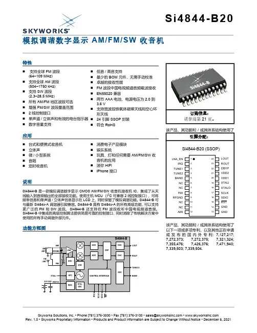
SkyworksSolutions,Inc.•Phone[781]376-3000•Fax[781]376-3100•*********************•Si4844-B20模拟调谐数字显示 AM/FM/SW 收音机特性功能方框图⏹ 支持全球 FM 波段(64–109MHz)⏹支持全球 AM 波段(504–1750kHz)⏹支持 SW 波段(2.3–28.5MHz)⏹所有 AM/FM 地区波段可选⏹增强 FM/SW 波段覆盖范围⏹ 2 线控制接口⏹单声道/立体声和有效的电台指示器⏹数字音量支持⏹低音/高音支持⏹最少的 BOM 元件,无需手动校准⏹卓越的接收性能⏹FM 波段中国电视频道音频载波接收⏹EN55020 兼容⏹两节 AAA 电池,电源电压为 2.0 到 3.6V⏹支持宽波段铁氧体磁棒天线和空心环形天线⏹24 引脚 SSOP 封装⏹符合 RoHS该产品、其功能和/或其体系结构使用了以下一项或多项专利,以及其他正在申请或发布的国内外专利:7,127,217;7,272,373; 7,272,375; 7,321,324;7,355,476; 7,426,376; 7,471,940;7,339,503; 7,339,504.订购信息:请参阅第 21 页。
Si4844-B202SkyworksSolutions,Inc.•Phone[781]376-3000•Fax[781]376-3100•*********************•Si4844-B20SkyworksSolutions,Inc.•Phone[781]376-3000•Fax[781]376-3100•*********************• 3T ABLE OF C ONTENTSSectionPage1. Electrical Specifications . . . . . . . . . . . . . . . . . . . . . . . . . . . . . . . . . . . . . . . . . . . . . . . . . . .42. Typical Application Schematic . . . . . . . . . . . . . . . . . . . . . . . . . . . . . . . . . . . . . . . . . . . .123. Bill of Materials . . . . . . . . . . . . . . . . . . . . . . . . . . . . . . . . . . . . . . . . . . . . . . . . . . . . . . . . .134. Functional Description . . . . . . . . . . . . . . . . . . . . . . . . . . . . . . . . . . . . . . . . . . . . . . . . . . .144.1. Overview . . . . . . . . . . . . . . . . . . . . . . . . . . . . . . . . . . . . . . . . . . . . . . . . . . . . . . . . . .144.2. FM Receiver . . . . . . . . . . . . . . . . . . . . . . . . . . . . . . . . . . . . . . . . . . . . . . . . . . . . . . .154.3. AM Receiver . . . . . . . . . . . . . . . . . . . . . . . . . . . . . . . . . . . . . . . . . . . . . . . . . . . . . . .154.4. SW Receiver . . . . . . . . . . . . . . . . . . . . . . . . . . . . . . . . . . . . . . . . . . . . . . . . . . . . . . .154.5. Frequency Tuning . . . . . . . . . . . . . . . . . . . . . . . . . . . . . . . . . . . . . . . . . . . . . . . . . . .164.6. Band Select . . . . . . . . . . . . . . . . . . . . . . . . . . . . . . . . . . . . . . . . . . . . . . . . . . . . . . . .164.7. Bass and Treble . . . . . . . . . . . . . . . . . . . . . . . . . . . . . . . . . . . . . . . . . . . . . . . . . . . .164.8. Volume Control . . . . . . . . . . . . . . . . . . . . . . . . . . . . . . . . . . . . . . . . . . . . . . . . . . . . .164.9. Stereo Audio Processing . . . . . . . . . . . . . . . . . . . . . . . . . . . . . . . . . . . . . . . . . . . . . .164.10. Stereo DAC . . . . . . . . . . . . . . . . . . . . . . . . . . . . . . . . . . . . . . . . . . . . . . . . . . . . . . .174.11. Soft Mute . . . . . . . . . . . . . . . . . . . . . . . . . . . . . . . . . . . . . . . . . . . . . . . . . . . . . . . . .174.12. Reference Clock . . . . . . . . . . . . . . . . . . . . . . . . . . . . . . . . . . . . . . . . . . . . . . . . . . .174.13. Reset, Powerup, and Powerdown . . . . . . . . . . . . . . . . . . . . . . . . . . . . . . . . . . . . . .174.14. Memorizing Status . . . . . . . . . . . . . . . . . . . . . . . . . . . . . . . . . . . . . . . . . . . . . . . . .174.15. Programming with Commands . . . . . . . . . . . . . . . . . . . . . . . . . . . . . . . . . . . . . . . .175. Commands and Properties . . . . . . . . . . . . . . . . . . . . . . . . . . . . . . . . . . . . . . . . . . . . . . . .186. Pin Description: Si4844-B . . . . . . . . . . . . . . . . . . . . . . . . . . . . . . . . . . . . . . . . . . . . . . . . .207. Ordering Guide . . . . . . . . . . . . . . . . . . . . . . . . . . . . . . . . . . . . . . . . . . . . . . . . . . . . . . . . . .218. Package Outline: Si4844-B20 . . . . . . . . . . . . . . . . . . . . . . . . . . . . . . . . . . . . . . . . . . . . . .229. PCB Land Pattern: Si4844-B20 . . . . . . . . . . . . . . . . . . . . . . . . . . . . . . . . . . . . . . . . . . . . .2310. Top Marking: Si4844-B20 . . . . . . . . . . . . . . . . . . . . . . . . . . . . . . . . . . . . . . . . . . . . . . . . .2411. Additional Reference Resources . . . . . . . . . . . . . . . . . . . . . . . . . . . . . . . . . . . . . . . . . .25Document Change List . . . . . . . . . . . . . . . . . . . . . . . . . . . . . . . . . . . . . . . . . . . . . . . . . . . . .26Si4844-B204SkyworksSolutions,Inc.•Phone[781]376-3000•Fax[781]376-3100•*********************•1. Electrical SpecificationsTable 1. Recommended Operating Conditions 1,2ParameterSymbol Test ConditionMin Typ Max Unit Supply Voltage 3V DD 2— 3.6V Power Supply Powerup Rise TimeV DDRISE10——µsNotes:1.Typical values in the data sheet apply at V DD =3.3V and 25°C unless otherwise stated.2. All minimum and maximum specifications in the data sheet apply across the recommended operating conditions forminimum V DD =2.7V.3. Operation at minimum V DD is guaranteed by characterization when V DD voltage is ramped down to 2.0V. Partinitialization may become unresponsive below 2.3V.Table 2. DC Characteristics(V DD =2.7 to 3.6V, TA =–15 to 85°C)ParameterSymbolTest ConditionMinTypMaxUnitFM ModeSupply Current 1I FM —21.0—mA Supply Current 2I FMLow SNR level—21.5—mAAM/SW ModeSupply Current 1I AM—20.0—mASupplies and InterfaceV DD Powerdown CurrentI DDPD—10—µANotes:1.Specifications are guaranteed by characterization.2. LNA is automatically switched to higher current mode for optimum sensitivity in weak signal conditions.Si4844-B20SkyworksSolutions,Inc.•Phone[781]376-3000•Fax[781]376-3100•*********************• 5Figure 1.Reset TimingTable 3. Reset Timing Characteristics(V DD = 2.7 to 3.6V, TA = –15 to 85°C)ParameterSymbol Min Typ Max Unit RSTB Pulse Widtht PRST 100——µs 2-wire bus idle time after RSTB risest SDIO 100——µs 2-wire bus idle time before RSTB rises, and VDD valid time before RSTB risest SRST 100——µs RSTB low time before VDD becomes invalidt RRST——µsNotes:1.RSTB must be held low for at least 100µs after the voltage supply has been ramped up.2. RSTB needs to be asserted (pulled low) prior to the supply voltage being ramped down.RSTBVDDSDIOSCLKSi4844-B206SkyworksSolutions,Inc.•Phone[781]376-3000•Fax[781]376-3100•*********************•Table 4. 2-Wire Control Interface Characteristics 1,2,3(V DD =2.7 to 3.6V, T A =–15 to 85°C)ParameterSymbol Test ConditionMin Typ Max Unit SCLK Frequency f SCLK 0—400kHz SCLK Low Time t LOW 1.3——µs SCLK High Timet HIGH 0.6——µs SCLK Input to SDIO ↓ Setup (START)t SU:STA 0.6——µs SCLK Input to SDIO ↓ Hold (START)t HD:STA 0.6——µs SDIO Input to SCLK ↑ Setup t SU:DAT 100——ns SDIO Input to SCLK ↓ Hold 4,5t HD:DAT 0—900ns SCLK input to SDIO ↑ Setup (STOP)t SU:STO 0.6——µs STOP to START Time t BUF 1.3——µs SDIO Output Fall Timet f:OUT—250nsSDIO Input, SCLK Rise/Fall Timet f:IN t r:IN—300nsSCLK, SDIO Capacitive Loading C b ——50pF Input Filter Pulse Suppressiont SP——50nsNotes:1.When V D =0V, SCLK and SDIO are low impedance.2. When selecting 2-wire mode, the user must ensure that a 2-wire start condition (falling edge of SDIO while SCLK ishigh) does not occur within 300ns before the rising edge of RST.3. When selecting 2-wire mode, the user must ensure that SCLK is high during the rising edge of RST, and stays highuntil after the first start condition.4. The Si484x delays SDIO by a minimum of 300ns from the V IH threshold of SCLK to comply with the minimum t HD:DATspecification.5. The maximum t HD:DAT has only to be met when f SCLK =400kHz. At frequencies below 400kHz, t HD:DAT may beviolated as long as all other timing parameters are met.200.1C b1pF----------+200.1C b1pF----------+Si4844-B20SkyworksSolutions,Inc.•Phone[781]376-3000•Fax[781]376-3100•*********************• 7Figure 2.2-Wire Control Interface Read and Write Timing ParametersFigure 3.2-Wire Control Interface Read and Write Timing DiagramTable 5. FM Receiver Characteristics 1,2(V DD =2.7 to 3.6V, TA =–15 to 85°C)ParameterSymbol Test ConditionMin Typ Max Unit Input Frequencyf RF64—109MHz Sensitivity with Headphone Network 3(S+N)/N = 26 dB —2.2—µV EMFNotes:1.Additional testing information is available in “AN603: Si4822/26/27/40/44 DEMO Board Test Procedure.”Volume =maximum for all tests. Tested at RF =98.1MHz.2. To ensure proper operation and receiver performance, follow the guidelines in “AN602: Si4822/26/27/40/44 Antenna,Schematic, Layout, and Design Guidelines.” Skyworks will evaluate schematics and layouts for qualified customers.3. Frequency is 64~109MHz.4. Guaranteed by characterization.5. V EMF =1 mV.6. F MOD =1kHz, MONO, and L =R unless noted otherwise.7. ∆f =22.5kHz.8. |f 2 – f 1| > 2MHz, f 0=2x f 1 – f 2.9. B AF =300Hz to 15kHz, A-weighted.10. At L OUT and R OUT pins.11. ∆f =75 kHz.12. Tested in Digital Volume Mode.SCLK70%30%SDIO70%30%STARTSTOP t f:INt r:INt LOWt HIGHt HD:STAt SU:STA t t t SU:DATt r:INHD:DATf:IN, t f:OUTSi4844-B208SkyworksSolutions,Inc.•Phone[781]376-3000•Fax[781]376-3100•*********************•LNA Input Resistance 4,5—4—k ΩLNA Input Capacitance 4,5—5—pF AM Suppression 4,5,6,7m = 0.3—50—dB Input IP34,8—105—dBµV EMFAdjacent Channel Selectivity 4±200 kHz —50—dB Alternate Channel Selectivity 4±400 kHz —65—dB Audio Output Voltage 5,6,7,12—80—mV RMS Audio Mono S/N 5,6,7,9,10—55—dB Audio Stereo S/N 3,4,5,7,9,10—55—dB Audio Frequency Response Low 4–3dB ——30Hz Audio Frequency Response High 4–3dB 15——kHz Audio Stereo Separation 5,11—40—dB Audio THD 5,6,11—0.10.5%Audio Output Load Resistance 4,10R L Single-ended 10——k ΩAudio Output Load Capacitance 4,10C LSingle-ended——50pFTable 5. FM Receiver Characteristics 1,2 (Continued)(V DD =2.7 to 3.6V, TA =–15 to 85°C)ParameterSymbolTest ConditionMin Typ Max Unit Notes:1.Additional testing information is available in “AN603: Si4822/26/27/40/44 DEMO Board Test Procedure.”Volume =maximum for all tests. Tested at RF =98.1MHz.2. To ensure proper operation and receiver performance, follow the guidelines in “AN602: Si4822/26/27/40/44 Antenna,Schematic, Layout, and Design Guidelines.” Skyworks will evaluate schematics and layouts for qualified customers.3. Frequency is 64~109MHz.4. Guaranteed by characterization.5. V EMF =1 mV.6. F MOD =1kHz, MONO, and L =R unless noted otherwise.7. ∆f =22.5kHz.8. |f 2 – f 1| > 2MHz, f 0=2x f 1 – f 2.9. B AF =300Hz to 15kHz, A-weighted.10. At L OUT and R OUT pins.11. ∆f =75 kHz.12. Tested in Digital Volume Mode.Si4844-B20SkyworksSolutions,Inc.•Phone[781]376-3000•Fax[781]376-3100•*********************• 9Table 6. AM/SW Receiver Characteristics 1, 2(V DD = 2.7 to 3.6 V, TA = –15 to 85 °C)ParameterSymbol Test Condition Min Typ Max Unit Input Frequencyf RFMedium Wave (AM)504— 1750kHz Short Wave (SW)2.3—28.5MHz Sensitivity 3,4,5(S+N)/N = 26 dB — 30—µV EMF Large Signal Voltage Handling 5THD < 8%— 300— mV RMS Power Supply Rejection Ratio 5ΔV DD =100 mV RMS , 100 Hz— 40— dB Audio Output Voltage 3,6,8— 60— mV RMS Audio S/N 3,4,6— 55— dB Audio THD 3,6— 0.10.5%Antenna Inductance 5,7180—450µHNotes:1.Additional testing information is available in “AN603: Si4822/26/27/40/44 DEMO Board Test Procedure.”Volume =maximum for all tests. Tested at RF =520kHz and RF =6MHz.2. To ensure proper operation and receiver performance, follow the guidelines in ““AN602: Si4822/26/27/40/44 Antenna,Schematic, Layout, and Design Guidelines.” Skyworks will evaluate schematics and layouts for qualified customers.3. FMOD =1kHz, 30% modulation, 2kHz channel filter.4. B AF =300Hz to 15kHz, A-weighted.5. Guaranteed by characterization.6. V IN =5mVrms.7. Stray capacitance on antenna and board must be <10pF to achieve full tuning range at higher inductance levels.8. Tested in Digital Volume Mode.Si4844-B2010SkyworksSolutions,Inc.•Phone[781]376-3000•Fax[781]376-3100•*********************•Table 7. Reference Clock and Crystal Characteristics(V DD = 2.7 to 3.6V, T A = –15 to 85°C)ParameterSymbolTest Condition MinTypMaxUnitReference ClockXTALI Supported Reference Clock Frequencies *31.13032.76840,000kHz Reference Clock Frequency Tolerance for XTALI–100—100ppmREFCLK_PRESCALE 14095REFCLK31.13032.76834.406kHz Crystal OscillatorCrystal Oscillator Frequency —32.768—kHz Crystal Frequency Tolerance –100—100ppm Board Capacitance——3.5pF*Note: The Si4844-B20 divides the RCLK input by REFCLK_PROSCALE to obtain REFCLK. There are some RCLKfrequencies between 31.130kHz and 40MHz that are not supported. For more details, see Table 9 of “AN610: Si48xx ATDD Programming Guide.”Table 8. Thermal ConditionsParameterSymbol Min Typ Max Unit Thermal Resistance* JA —80—°C/W Ambient Temperature T A –152585°C Junction TemperatureT J——92°C*Note: Thermal resistance assumes a multi-layer PCB with the exposed pad soldered to a topside PCB pad.Si4844-B20Table 9. Absolute Maximum Ratings 1, 2Parameter Symbol Value UnitSupply Voltage V DD–0.5 to 5.8VInput Current3I IN10mAOperating Temperature T OP–40 to 95︒CStorage Temperature T STG–55 to 150︒CRF Input Level40.4V PKNotes:1.Permanent device damage may occur if the above Absolute Maximum Ratings are exceeded. Functional operationshould be restricted to the conditions as specified in the operational sections of this data sheet. Exposure beyond recommended operating conditions for extended periods may affect device reliability.2. The Si4844-B devices are high-performance RF integrated circuits with certain pins having an ESD rating of < 2kVHBM. Handling and assembly of these devices should only be done at ESD-protected workstations.3. For input pins RST, SDIO, SCLK, XTALO, XTALI, BAND, TUNE2, TUNE1, IRQ, and LNA_EN.4. At RF input pins, FMI, and AMI.Si4844-B202. Typical Application SchematicNotes:1.Place C4 close to V DD2 and DBYP pins.2. All grounds connect directly to GND plane on PCB.3. Pin 6 and 7 leave floating.4. To ensure proper operation and receiver performance, follow the guidelines in “AN602: Si4822/26/27/40/44 Antenna,Schematic, Layout, and Design Guidelines.” Skyworks will evaluate the schematics and layouts for qualified customers.5. Pin 8 connects to the FM antenna interface and pin 12 connects to the AM antenna interface.6. Place Si484x as close as possible to antenna jack and keep the FMI and AMI traces as short as possible.7. Recommend keeping the AM ferrite loop antenna at least 5cm away from the Si4844-B.8. Keep the AM ferrite loot antenna away from the MCU, audio amplifier, and other circuits which have AM interference.9. Place the transformer T1 away from any sources of interference and even away from the I/O signals of the Si4844-B.Si4844-B20 3. Bill of MaterialsTable 10. Si4844-B20 Bill of MaterialsComponent(s)Value/Description Supplier C1Reset capacitor 0.1µF, ±20%, Z5U/X7R MurataC4Supply bypass capacitor, 0.1µF, ±20%, Z5U/X7R MurataC5Coupling capacitor, 0.47µF, ±20%, Z5U/X7R MurataB1Ferrite bead 2.5k/100MHz MurataVR1Variable resistor (POT), 100k, ±10% KennonU1Si4844-B AM/FM/SW Analog Tune Digital Display Radio Tuner SkyworksANT1Ferrite stick,180–450μH JiaxinOptional ComponentsC2, C3Crystal load capacitors, 22pF, ±5%, COGVenkel(Optional: for crystal oscillator option)Y132.768kHz crystal (Optional: for crystal oscillator option)Epson or equivalentANT2Air loop antenna, 10-20μH variousS1Band switch Any, depends on customerR1Resistor, 203k, ±1%VenkelR2Resistor, 50k, ±1%VenkelR3Resistor, 180k, ±1%VenkelR4Resistor, 67k, ±1%VenkelSi4844-B204. Functional DescriptionFigure4.Si4844-B Functional Block Diagram4.1. OverviewThe Si4844-B is the analog-tuned digital-display digital CMOS AM/FM/SW radio receiver IC that integrates the complete receiver function from antenna input to audio output. Working with an external MCU with LCD/LED driver, Si4844-B can output the AM/FM/SW frequencies, band, Bass/Treble and stereo/mono information to display on LCD/LED, while using a simple potentiometer at the front end for analog-tune. Leveraging Skyworks' proven and patented digital low intermediate frequency (low-IF) receiver architecture, the Si4844-B delivers superior RF performance and interference rejection in AM, FM and SW bands. The Si4844-B is pin-to-pin compatible with the current Si484x-A tuning. The Si4844-B shares the advanced features of the Si484x-A and can support a wider range of FM and SW bands. It also supports China TV channels and audio reception in the FM band. The superior control algorithm integrated in Si4844-B provides an easy and reliable control interface while eliminating all the manually tuned external components used in traditional solutions.Like other successful audio products from Skyworks, Si4844-B offers unmatched integration and PCB space savings with minimum external components and small board area on a single side PCB. The high integration and complete system production test simplifies design-in, increases system quality, and improves manufacturability. The receiver has very low power consumption, runs off two AAA batteries, and delivers the performance benefits of high performance digital radio experience with digital display to the legacy analog-tuned radio market.The Si4844-B provides good flexibility in using the chip. The frequency range of FM/AM/SW bands, mono/stereo threshold, de-emphasis value, AM tuning step, AM soft mute level/rate, and Bass/Treble can be either configured by the MCU or by using external hardware to make a selection. The reference clock of the FM tuner can be provided either by the crystal or by the host MCU within tolerance.Si4844-B also has flexibility in selecting bands and configuring band properties, enabling masked Host MCU for multiple projects, and reducing the cost of development. Four tuning preferences are available tomeet different tuning preference requirements.4.2. FM ReceiverThe Si4844-B integrates a low noise amplifier(LNA) supporting the worldwide FM broadcast band (64to 109MHz) and the TV audio stations within the fre quency range in China are also supported. The FM band can also be configured to be a wider range such as 64–108 MHz in one band.Pre-emphasis and de-emphasis is a technique used by FM broadcasters to improve the signal-to-noise ratio of FM receivers by reducing the effects of high frequency interference and noise. When the FM signal is transmitted, a pre-emphasis filter is applied to accentuate the high audio frequencies. All FM receivers incorporate a de-emphasis filter which attenuates high frequencies to restore a flat frequency response. Two time constants are used in various regions. The de-emphasis time constant can be chosen to be 50 or 75μs. Refer to “AN602: Si4822/26/27/40/44 Antenna, Schematic, Layout, and Design Guidelines.”The Si4844-B also has advanced stereo blending that employs adaptive noise suppression. As a signal quality degrades, the Si4844-B gradually combines the stereo left and right audio channels to a mono audio signal to maintain optimum sound fidelity under varying reception conditions. The Si4844-B can output a stereo signal to MCU with LCD/LED driver to display on the LCD/LED so that the user can easily discern the signal quality.The stereo on signal is defined using both RSSI and the Left and Right separation levels as these two specifications are the primary factors for stereo listening. The criteria can be set between two conditions: the Left and Right channels are separated by more than 6dB with RSSI at >20dB or Left and Right channels are separated by more than 12dB with RSSI at >28dB. The selection can be set up using different values of the external resistor or configured by the host MCU. Refer to “AN602: Si4822/26/27/40/44 Antenna, Schematic, Layout, and Design Guidelines.”The user can also refer to the “AN610: Si48xx ATDD Programming Guide” for those who want to configure the value by host MCU.4.3. AM ReceiverThe highly integrated Si4844-B supports worldwide AM band reception from 504 to 1750kHz with five sub-bands using a digital low-IF architecture with a minimum number of external components and no manual alignment required. This patented architecture allows for high-precision filtering, offering excellent selectivity and SNR with minimum variation across the AM band. Similar to the FM receiver, the Si4844-B optimizes sensitivity and rejection of strong interferers, allowing better reception of weak stations.To offer maximum flexibility, the receiver supports a wide range of ferrite loop sticks from 180–450μH. An air loop antenna is supported by using a transformer to increase the effective inductance from the air loop. Using a 1:5 turn ratio inductor, the inductance is increased by 25 times and easily supports all typical AM air loop antennas, which generally vary between 10 and 20μH.A 9, 10kHz tuning step can be chosen by the external resistor or host MCU according to the different regions, and AM soft mute level can be programmed by the host MCU to have different tuning experiences. One of the AM bands can be configured as a universal AM band that simultaneously supports 9kHz and 10kHz channel spaces for all regional AM standards worldwide. Refer to “AN610: Si48xx ATDD Programming Guide” and “AN602: Si4822/26/27/40/44 Antenna, Schematic, Layout, and Design Guidelines”for more details.4.4. SW ReceiverThe Si4844-B supports short wave band receptions from 2.3 to 28.5MHz in 5kHz step size increments. It can also be configured to have a wide SW band that can be used in SW radio with 1 or 2 SW banks. Si4844-B supports extensive short wave features such as minimal discrete components and no factory adjustments. The Si4844 supports using the FM antenna to capture short wave signals. Refer to “AN610: Si48xx ATDD Programming Guide”and “AN602: Si4822/26/27/40/44 Antenna, Schematic, Layout, and Design Guidelines”for more details.4.5. Frequency TuningA valid channel can be found by tuning the potentiometer that is connected to the TUNE1 and TUNE2 pin of the Si4844-B chip.To offer easy tuning, the Si4844-B also outputs the tuned information to the MCU with LCD/LED driver to display. It will light up the icon on display if the RF signal quality passes a certain threshold when tuned to a valid station. Multiple tuning preferences are available. The user can choose to have the best performance (volume, stereo/mono effect) only at the exact channel, or the best performance in a larger range. Refer to "AN610: Si48xx ATDD Programming Guide" for more details. 4.6. Band SelectThe Si4844-B supports worldwide AM band with five sub-bands, US/Europe/Japan/China FM band with five sub-bands, and SW band with 16 sub-bands. Si4844-B provides the flexibility to configure the band and band properties at either the MCU side or the Tuner side, enabling masked MCU for multiple projects. For details on band selection, refer to “AN602: Si4822/26/27/40/44 Antenna, Schematic, Layout, and Design Guidelines”and "AN610: Si48xx ATDD Programming Guide".4.7. Bass and TrebleThe Si4844-B further supports Bass/Treble tone control for superior sound quality. The Si4844-B can be set to be default normal, or programmed by the host MCU I2C-compatible 2-wire mode. FM has nine levels Bass/Treble effect and AM/SW has seven levels Bass/Treble effect. For further configuration details, refer to "AN610: Si48xx ATDD Programming Guide." 4.8. Volume ControlThe Si4844-B not only allows users to use the traditional PVR wheel volume control through an external speaker amplifier, it also supports digital volume control programmed by the host MCU. Si4844-B can be programmed to be Bass/Treble mode only or digital volume mode only; it can also be programmed to have the digital volume coexist with Bass/Treble in two modes. Refer to "AN610: Si48xx ATDD Programming Guide" and “AN602: Si4822/26/27/40/44 Antenna, Schematic, Layout, and Design Guidelines” for more details.4.9. Stereo Audio ProcessingThe output of the FM demodulator is a stereo multiplexed (MPX) signal. The MPX standard was developed in 1961, and is used worldwide. Today's MPX signal format consists of left + right (L+R) audio, left – right (L–R) audio, a 19kHz pilot tone.Figure5.MPX Signal Spectrum4.9.1. Stereo DecoderThe Si4844-B's integrated stereo decoder automatically decodes the MPX signal using DSP techniques. The 0 to 15kHz (L+R) signal is the mono output of the FM tuner. Stereo is generated from the (L+R), (L–R), and a 19kHz pilot tone. The pilot tone is used as a reference to recover the (L–R) signal. Output left and right channels are obtained by adding and subtracting the (L+R) and (L–R) signals respectively.4.9.2. Stereo-Mono BlendingAdaptive noise suppression is employed to gradually combine the stereo left and right audio channels to a mono (L+R) audio signal as the signal quality degrades to maintain optimum sound fidelity under varying reception conditions. Three metrics, received signal strength indicator (RSSI), signal-to-noise ratio (SNR), and multipath interference, are monitored simultaneously in forcing a blend from stereo to mono. The metric which reflects the minimum signal quality takes precedence and the signal is blended appropriately.All three metrics have programmable stereo/mono thresholds and attack/release rates. If a metric falls below its mono threshold, the signal is blended from stereo to full mono. If all metrics are above their respective stereo thresholds, then no action is taken to blend the signal. If a metric falls between its mono and stereo thresholds, then the signal is blended to the level proportional to the metric’s value between its mono and stereo thresholds, with an associated attack and release rate.0575338231915Frequency (kHz)ModulationLevel4.10. Stereo DACHigh-fidelity stereo digital-to-analog converters (DACs) drive analog audio signals onto the LOUT and ROUT pins. The audio output may be muted.4.11. Soft MuteThe soft mute feature is available to attenuate the audio outputs and minimize audible noise in very weak signal conditions. An advanced algorithm is implemented to get a better analog tuning experience. The soft mute feature is triggered by the SNR metric. The SNR threshold for activating soft mute is programmable, as are soft mute attenuation levels and attack and decay rates.4.12. Reference ClockThe Si4844-B supports programmable RCLK input (to XTALI pin) with the spec listed in Table7. It can be shared with the host MCU to save extra crystal.An onboard crystal oscillator is available to generate the 32.768kHz reference when an external crystal and load capacitors are provided. Refer to "AN602: Si4822/26/27/40/44 Antenna, Schematic, Layout, and Design Guidelines" for more details.4.13. Reset, Powerup, and Powerdown Setting the RSTB pin low will disable analog and digital circuitry, reset the registers to their default settings, and disable the bus. Setting the RSTB pin high will bring the device out of reset.Figure1 shows typical reset, startup, and shutdown timings for the Si4844-B. RSTB must be held low (asserted) during any power supply transitions and kept asserted as specified in Figure1 after the power supplies are ramped up and stable. Failure to assert RSTB as indicated here may cause the device to malfunction and may result in permanent device damage.A powerdown mode is available to reduce power consumption when the part is idle. Putting the device in powerdown mode will disable analog and digital circuitry while keeping the bus active.4.14. Memorizing StatusThe Si4844-B provides the feature to memorize status from the last power down with a simple design on PCB, including frequency of the FM/AM/SW station. Refer to “AN602: Si4822/26/27/40/44 Antenna, Schematic, Layout, and Design Guidelines”for details.4.15. Programming with CommandsTo ease development time and offer maximum customization, the Si4844-B provides a simple yet powerful software interface to program the receiver. The device is programmed using commands, arguments, properties, and responses.To perform an action, the user writes a command byte and associated arguments, causing the chip to execute the given command. Commands control an action such as powerup the device, shut down the device, or get the current tuned frequency. Arguments are specific to a given command and are used to modify the command. Properties are a special command argument used to modify the default chip operation and are generally configured immediately after powerup. Examples of properties are de-emphasis and soft mute attenuation threshold.Responses provide the user information and are echoed after a command and associated arguments are issued. All commands provide a 1-byte status update, indicating interrupt and clear-to-send status information. For a detailed description of the commands and properties for the Si4844-B, see "AN610: Si48xx ATDD Programming Guide."。
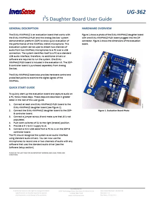
UG-362 I2S Daughter Board User GuideGENERAL DESCRIPTIONThe EVAL-INMP441Z is an evaluation board that works with the EVAL-INMP441Z-FLEX and the Analog Devices’ system demonstration platform (SDP) to allow quick evaluation of the performance of the INMP441 MEMS microphone. This evaluation system can be used to stream two channels of audio from two INMP441 microphones to a PC over a USB connection. The system identifies itself to a PC as a standard USB audio interface; therefore, no additional drivers or software are required to run the system. One EVAL-INMP441Z-FLEX board is included in the evaluation kit. The SDP-B controller board is purchased separately from Analog Devices.The EVAL-INMP441Z board also provides hardware control and probe/test points to examine the digital signals of theINMP441.QUICK START GUIDETo quickly start up the evaluation board and capture audio on a PC, follow these steps. These steps are described in greater detail in the rest of this user guide.1.Connect at least one EVAL-INMP441Z-FLEX board to theEVAL-INMP441Z daughter board (see Figure 1).2.Connect the EVAL-INMP441Z daughter board to the SDP-B controller board.3.Connect a jumper across J9 and make sure that J8 is notpopulated.4.Push both switches of S1 to the right (enable) position.5.Provide a 5 V to 6 V supply to J4.6.Connect a mini-USB cable from a PC to J1 on the SDP-Bcontroller board.The PC should recognize the system as an audio interface using standard audio drivers. You can now use the microphones to record one or two channels of audio with any software that uses the standard audio driver (see the Software Setup section).PLEASE SEE THE LAST PAGE FOR AN IMPORTANT WARNING AND LEGAL TERMS AND CONDITIONS.HARDWARE OVERVIEWFigure 1 shows a photo of the EVAL-INMP441Z daughter board with one EVAL-INMP441Z-FLEX board plugged into the ZIF connector. Figure 2 shows the dimensions of the evaluation board.Figure 1. Evaluation Board Photo 1432-1InvenSense reserves the right to change the detail specifications as may be required to permitimprovements in the design of its products.InvenSense Inc.1745 Technology Drive, San Jose, CA 95110 U.S.A+1(408) 988–7339Document Number: UG-362-00Revision: 1.1Rev Date: 04/28/2014UG-362Dimensions shown in millimetersSETTING UP THE EVALUATION BOARDHARDWARE SETUP PowerThe EVAL-INMP441Z board is powered with a single 5 V to 6 V supply from either Barrel Connector J4 or Pin Header J5. The dc supply connected to J4 should be positive-tip. The micro-phones are configured to run with a single 1.8 V supply, but the supply can be set to either 2.5 V or 3.3 V by mounting a 0 Ω resistor on R17 or R11, respectively, and removing R18.LED D1 is illuminated when the board is powered on. With V DD = 1.8 V, the LED is only faintly lit.Power is supplied to the EVAL-INMP441Z-FLEX board through Voltage Regulator U5.The power supply connected to the EVAL-INMP441Z board also powers the SDP-B controller board through Connector J3. The microphone board requires only a few milliamps of current, but the SDP-B controller board requires up to 200 mA at 5 V.JumpersThe J8 and J9 jumper headers on the EVAL-INMP441Z board set the clock source and select the boot code.Header J8 does not need to be shorted with a jumper for the default clocking configuration. When J8 is populated, the 3.072 MHz crystal on the EVAL-INMP441Z board generates the master clock for the SPORT interface of the Blackfin® processor. By default, however, the microphone clocks are generated on the Blackfin processor.Header J9 selects the source of the code to boot the Blackfin processor on the SDP-B controller board. To use theevaluation system to stream USB audio to a PC, a jumper must be shorted across Header J9. Without the jumperpresent, the Blackfin processor boots the standard SDP code and does not perform USB streaming audio.These settings for J8 and J9 are illustrated in Figure 3.Figure 3. Top View of EVAL-IN MP441Z Board with Default Switchand Jumper Settings10432-00210432-003Document Number: UG-362--00 Page 2 of 9Revision: 1.1Rev Date: 04/28/2014UG-362SwitchesSwitch Block S1 has two SPST switches to control the CHIPEN pins of the two INMP441 microphones. When the switches are in the left position, the microphones are disabled; when the switches are in the right position, the microphones are enabled. Switch 1 (bottom switch) controls the leftmicrophone, and Switch 2 (top switch) controls the right microphone. The switch settings in Figure 3 show the microphones enabled.Flex Board ConnectionsThe EVAL-INMP441Z daughter board includes two headers, J1 and J2, to connect two INMP441 microphone flex boards (EVAL-INMP441Z-FLEX). The EVAL-INMP441Z-FLEX board connects all the pins of the INMP441 to copper contacts on the edge of the flex board.The EVAL-INMP441Z-FLEX board can be inserted directly into a ZIF connector, such as J1 or J2 on the EVAL-INMP441Zboard. A microphone connected to Header J1 is configured tooutput its data to the left channel of the I 2S data stream, and the microphone connected to Header J2 is configured to output its data to the right channel.The EVAL-INMP441Z-FLEX boards slide easily into the ZIF connectors on the EVAL-INMP441Z board. Follow these steps to install the flex boards.1. Loosen the black clamp on the J1 or J2 connector bypulling it to the right.2. Insert the flex board into the connector with the coppercontacts facing down.3. After the flex board is fully inserted, tighten the blackclamp to fasten the flex board in the connector. When properly connected, the sound port of the microphone is pointed up (see Figure 4). When two flex boards areconnected, the microphone sound ports are spaced 21 mm apart.Figure 4. EVAL-INMP441Z with Two Flex Boards Connected to an SDP-B Controller BoardSDP-B ConnectionThe EVAL-INMP441Z board connects to the Blackfin SDP-B controller board through Connector J3. The EVAL-INMP441Z board can be connected to either CON A or CON B on the SDP-B controller board; these two connectors provideidentical functionality. After you connect the EVAL-INMP441Z board to the SDP-B controller board but before you connect the USB jack of the SDP-B board to a PC, connect the power to the EVAL-INMP441Z board. After the system is powered on, you can connect the USB cable between the PC and J1 on the SDP-B controller board.The EVAL-INMP441Z board connects to the SDP-B controller board using a Hirose FX8-120P-SV1(91) connector on the SDP-B board. For more information about the SDP-B controller board, see the SDP User Guide (UG-277).The ADSP-BF527 Blackfin DSP on the SDP-B controller board is booted from code stored in the SPI flash memory IC (U7) on the EVAL-INMP441Z board.10432-004Document Number: UG-362--00 Page 3 of 9Revision: 1.1Rev Date: 04/28/2014UG-362I2S Monitoring HeaderThe I2S signal output from the INMP441 microphones canbe monitored on Header J7. The WS and SCK clock signals aresupplied from the SDP-B controller board, whereas the SDdata signal is output from the microphones. Note that HeaderJ7 cannot be used to supply clocks directly to themicrophones because the level translator (U6) is configuredto always drive the clock signals.SOFTWARE SETUPThe SDP-B/EVAL-INMP441Z system does not require newsoftware to be installed on the PC. The system identifies itselfas a standard audio class device and uses the standardWindows® audio drivers. Therefore, the system can be usedby any PC software that can record audio through thestandard drivers.The EVAL-INMP441Z board is identified in the WindowsDevice Manager as INMP441 USB Audio (see Figure 5).One or two channels of audio can be recorded at a samplerate of 48 kHz.Figure 5. Windows Device ManagerThe evaluation system functions as a USB audio device inWindows XP, Windows Vista®, and Windows 7. The PC audiosettings show both a Microphone and a Line setting forINMP441 USB Audio. These items have identical function-ality; either can be selected with no functional differences.The sensitivity of the IN MP441 is −26 dBFS. If the microphoneis used to record voices at normal conversational levels, thelevel of the recording may be somewhat low. To boost thelevel of the recorded audio, try applying gain to the signal in therecord path of the recording software (a gain of 10 dB to 20 dB isrecommended).The following sections provide instructions for setting upseveral popular software tools to listen and record with theEVAL-INMP441Z system.Windows Sound SettingsYou can control the properties of the INMP441 USB audiodevice in Windows as follows. (The following steps and thescreenshot in Figure 6 are for Windows 7. For other versionsof Windows software, this procedure may vary.)1.Right-click the speaker icon in the taskbar and selectRecording devices.2.Ensure that the IN MP441 USB audio microphone device isenabled and active.3.Select Properties for the device to display the MicrophoneProperties window.4.In the Microphone Properties window, click the Listen tab(see Figure 6).Figure 6. Windows Microphone Properties Window5.Select the box labeled Listen to this device and click Apply.The Listen to this device option allows you to loop themicrophone audio back to the audio output of the PC,either through the internal speakers or throughexternally connected headphones or speakers.1432-51432-6Document Number: UG-362--00 Page 4 of 9Revision: 1.1Rev Date: 04/28/2014UG-362You should now be able to hear the microphone audiodirectly on the PC audio output. If you are using speakersinstead of headphones with your PC, do not place themicrophones too close to the speakers because audiblefeedback can be created.Audacity Sound SettingsAudacity® is a free audio recording and editing tool. To recordaudio using the EVAL-INMP441Z system, you can select eitherMicrophone (INMP441 USB Audio) or Line (INMP441 USBAudio) as the recording device in the Audacity Preferenceswindow (see Figure 7). The version tested was Audacity 1.3.Figure 7. Audacity Preferences WindowAdobe Audition SettingsAudition® is the Adobe® multitrack audio recording tool. Torecord audio using the EVAL-INMP441Z system, you canselect either Microphone (INMP441 USB Audio) or Line(INMP441 USB Audio) as the default input in the AuditionPreferences window (see Figure 8). The version tested wasAdobe Audition CS5.5.Figure 8. Adobe Audition Preferences Window1432-71432-8Document Number: UG-362--00 Page 5 of 9Revision: 1.1Rev Date: 04/28/2014UG-362EVALUATION BOARD SCHEMATICFigure 9. Schematic of the Evaluation Board74L V C 125A _S S O P 141Document Number: UG-362--00 Page 6 of 9Revision: 1.1Rev Date: 04/28/2014UG-362TABLE 1. BILL OF MATERIALSQTY REFERENCE DESCRIPTION MANUFACTURER PART NUMBER6 C1 to C6 Capacitor, multilayer ceramic, 1 μF, 16 V, X7R, 0603 Taiyo Yuden EMK107BJ105KA-TR 2 C7, C8 Capacitor, multilayer ceramic, 27 pF, 50 V, NP0,0402 Murata ENA GRM1555C1H270JZ01D 2 C9, C10 Capacitor, SMD tantalum, 10 μF, 6.3 V, 0805 Rohm TCP0J106M8R8 C11 to C14,C19 to C22 Capacitor, multilayer ceramic, 0.10 μF, 16 V, X7R,0402 Panasonic EC ECJ-0EX1C104K1 C15 Capacitor, multilayer ceramic, 0.10 μF, 16 V, X7R,0402 (not installed) Panasonic EC ECJ-0EX1C104K3 C16 to C18 Capacitor, multilayer ceramic, 22 pF, 50 V, NP0,0402 Murata ENA GRM1555C1H220JZ01D1 D1 Diode, green diffused, 10 mcd, 565 nm, 1206 Lumex Opto SML-LX1206GW-TR2 D2, D3 Schottky diode, 30 V, 0.5 A, SOD-123 On Semiconductor MBR0530T1G2 J1, J2 FPC connector, 1 × 10-pin, surface mount, horizontal AMP 1-84952-01 J3 120-way connector, 0.6 mm pitch Hirose FX8-120S-SV1 J4 Mini power jack, 0.08”, R/A, T/H Switchcraft, Inc. RAPC722X1 J5 2-pin header, unshrouded jumper, 0.10” Sullins ConnectorSolutions PBC02SAAN1 J6 10-way, shrouded polarized header,2 × 5 (notinstalled) 3M N2510-6002RB1 J7 6-way, unshrouded header,2 ×3 Sullins ConnectorSolutions PBC03DAAN2 J8, J9 2-pin header, unshrouded jumper, 0.10”; use shuntTyco 881545-2 Sullins ConnectorSolutions PBC02SAAN5 R1, R2, R12,R19, R27 Chip resistor, 10 kΩ, 1%, 63 mW, thick film, 0402Rohm MCR01MZPF1002 3 R3, R4, R18 Chip resistor, 0 Ω, 5%, 100 mW, thick film, 0402 Panasonic EC ERJ-2GE0R00X 3 R5, R6, R22 Chip resistor, 100 kΩ, 1%, 63 mW, thick film, 0402Rohm MCR01MZPF100313 R7 to R9, R11,R17, R20, R21,R23 to R26,R28, R29Do not install1 R10 Chip resistor, 68.1 Ω, 1%, 63 mW, thick film, 0402Yageo RC0402FR-0768R1L2 R30, R31 Chip resistor, 2.67 kΩ, 1%, 63 mW, thick film, 0402;do not install Vishay/Dale CRCW04022K67FKEDDocument Number: UG-362--00 Page 7 of 9Revision: 1.1Rev Date: 04/28/2014UG-362QTY REFERENCE DESCRIPTION MANUFACTURER PART NUMBER1 R32 Chip resistor, 1 MΩ, 1%, 63 mW, thick film, 0402Rohm MCR01MZPF1004 1 R33 Chip resistor, 1.3 kΩ, 1%, 63 mW, thick film, 0402Vishay/Dale CRCW04021K30FKED 1 R34 Chip resistor, 2 kΩ, 1%, 100 mW, thick film, 0402 Panasonic EC ERJ-2RKF2001X3 R35 to R37 Chip resistor, 100 Ω, 1%, 63 mW, thick film, 0402Rohm MCR01MZPF1000 1 S1 2-section SPST SMD dip switch, raised actuator CTS Corp 219-2LPST8 TP1 to TP8 Mini test point, white, 0.1” OD Keystone Electronics 50021 U1 256 kb I2C CMOS serial EEPROM Microchip 24AA256-I/ST2 U2, U3 Inverter, SGL TinyLogic, SOT-23 Fairchild Semiconductor NC7SZ04M5X1 U4 IC, quad buffer, three-state, 14-TSSOP Texas Instruments 74LVC125APWT1 U5 Fixed triple-output low dropout voltage regulator Analog Devices, Inc. ADP322ACPZ-135-R7 1 U6 IC, bidirectional volt-level translator, 16-DQFN Fairchild Semiconductor FXL4TD245BQX1 U7 32 Mb serial flash Numonyx (Micron) M25P32-VMW6G 1 Y1 Crystal, 3.072 MHz, SMT, 18 pF Abracon ABLS-LR-3.072MHZ-TSUPPORTING DOCUMENTSUG-303: User Guide, EVAL-INMP441Z-FLEX: Bottom-Port I2S Output MEMS Microphone Evaluation BoardUG-277: Analog Devices User Guide, SDP-B Controller BoardESD CAUTIONESD (electrostatic discharge) sensitive device.Charged devices and circuit boards candischarge without detection. Although thisproduct features patented or proprietaryprotection circuitry, damage may occur ondevices subjected to high energy ESD.Therefore proper ESD precautions should betaken to avoid performance degradation orloss of functionality. EVALUATION KIT CONTENTS EV_INMP441 Daughter BoardEV_INMP441-FX Board5 V Power SupplyDocument Number: UG-362--00 Page 8 of 9 Revision: 1.1Rev Date: 04/28/2014UG-362COMPLIANCE DECLARATION DISCLAIMERInvenSense believes the environmental and other compliance information given in this document to be correct but cannot guarantee accuracy or completeness. Conformity documents substantiating the specifications and component characteristics are on file. InvenSense subcontracts manufacturing and the information contained herein is based on data received from vendors and suppliers, which has not been validated by InvenSense.This information furnished by InvenSense is believed to be accurate and reliable. However, no responsibility is assumed by InvenSense for its use, or for any infringements of patents or other rights of third parties that may result from its use. Specifications are subject to change without notice. InvenSense reserves the right to make changes to this product, including its circuits and software, in order to improve its design and/or performance, without prior notice. InvenSense makes no warranties, neither expressed nor implied, regarding the information and specifications contained in this document. InvenSense assumes no responsibility for any claims or damages arising from information contained in this document, or from the use of products and services detailed therein. This includes, but is not limited to, claims or damages based on the infringement of patents, copyrights, mask work and/or other intellectual property rights.Certain intellectual property owned by InvenSense and described in this document is patent protected. No license is granted by implication or otherwise under any patent or patent rights of InvenSense. This publication supersedes and replaces all information previously supplied. Trademarks that are registered trademarks are the property of their respective companies. InvenSense sensors should not be used or sold in the development, storage, production or utilization of any conventional or mass-destructive weapons or for any other weapons or life threatening applications, as well as in any other life critical applications such as medical equipment, transportation, aerospace and nuclear instruments, undersea equipment, power plant equipment, disaster prevention and crime prevention equipment.©2014 InvenSense, Inc. All rights reserved. InvenSense, MotionTracking, MotionProcessing, MotionProcessor, MotionFusion, MotionApps, DMP, AAR, and the InvenSense logo are trademarks of InvenSense, Inc. Other company and product names may be trademarks of the respective companies with which they are associated.©2014 InvenSense, Inc. All rights reserved.Document Number: UG-362--00Revision: 1.1Rev Date: 04/28/2014。
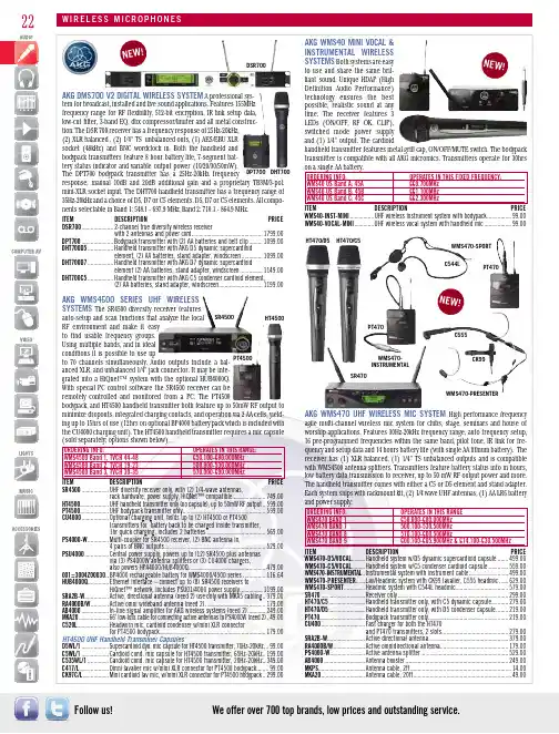
22Follow us!AKG WMS470 UHF WIREL agile multi-channel wireless mic system for clubs, stage, seminars and house of worship applications. Features 30Hz-20kHz frequency range, auto frequency setup, 16 pre-programmed frequencies within the same band, pilot tone, IR link for fre-quency and setup data and 14 hours battery life (with single AA lithium battery). The receiver has (1) XLR balanced, (1) 1/4" TS unbalanced outputs and is compatible with WMS4500 antenna splitters. Transmitters feature battery status info in hours, low battery data transmission to receiver, up to 50 mW RF output power and more. The handheld transmitter comes with either a C5 or D5 element and stand adapter. Each system ships with rackmount kit, (2) 1/4 wave UHF antennas, (1) AA LR6 battery and power supply.ORDERING INFO: WMS470 BAND 1 WMS470 BAND 7 WMS470 BAND 8 WMS470 BAND 9 ITEM DESCRIPTION WMS470-D5/VOCAL .........Handheld system w/D5 dynamic supercardioid capsule .......WMS470-C5/VOCAL .........Handheld system w/C5 condenser cardioid capsule .............WMS470-INSTRUMENTAL ..Instrumental system with instrument cable WMS470-PRESENTER v/Headmic system with CK99 lavalier, C555 headmic ......WMS470-SPORT ..............Headmic system with C544L headmic SR470 .............................Receiver only .........................................................................HT470/C5 ........................Handheld transmitter only, with C5 dynamic capsule HT470/D5 ........................Handheld transmitter only, with D5 condenser capsule PT470..............................Bodypack transmitter only CU400 .............................Fast charger for both the HT470 and PT470 transmitters, 2 slots SRA2B-W .........................Active directional antenna.....................................................RA4000B/W .....................Active omnidirectional antenna PS4000-W .......................Active antenna splitter AB4000 ...........................Antenna booster ....................................................................MKPS ...............................Antenna cable, 2ft MKA20 .............................Antenna cable, 20ft ESStechnology ensures the bestswitched mode power supplyN E W !HT470/D5C544L C555WMS470-INSTRUMENTAL WMS470-PRESENTER WMS470-SPORTPT470CK99PT470SR470We offer over 700 top brands, low prices and outstanding service.A professional sys-tem for broadcast, installed and live sound applications. Features 155MHz frequency range for RF flexibility, 512-bit encryption, IR link setup data, low-cut filter, 3-band EQ, dbx compressor/limiter and all metal construc-N E W !DSR700AKG WMS4500 SERIES UHF WIRE ESSThe SR4500 diversity receiver featuresauto-setup and scan functions that analyze the local RF environment and make it easyto find usable frequency groups.grated into a HiQnet™ system with the optional HUB4000Q.With special PC control software the SR4500 receiver can beremotely controlled and monitored from a PC. The PT4500bodypack, and HT4500 handheld transmitter both feature up to 50mW RF output to minimize dropouts, integrated charging contacts, and operation via 2 AA cells, yield-ing up to 15hrs of use (12hrs on optional BP4000 battery pack which is included with the CU4000 charging unit). The HT4500 handheld transmitter requires a mic capsule (sold separately; options shown below).OPERATES IN THIS RANGE:WMS4500 Band 1, TVCH 44-48 650.100-680.000MHzWMS4500 Band 2, TVCH 19-23 500.000-530.000MHzWMS4500 Band 3, TVCH 30-35 570.000-600.000MHzITEM DESCRIPTION PRICE ..................UHF diversity receiver only, with (2) 1/4-wave antennas,rack hardware, power supply, HiQNet™ compatible ......................749.00...................UHF handheld transmitter only (no capsule), up to 50mW RF output ..599.00...................UHF bodypack transmitter only .......................................................599.00..................Optional charging unit, holds up to (2) HT4500 or PT4500transmitters for battery back to be charged inside transmitter,1hr quick charging, includes 2 batteries .......................................569.00.............Multi-coupler for SR4500 receiver, (2) BNC antenna in,4 pairs of BNC outputs ...................................................................529.00................Central power supply, powers up to (12) SR4500 plus antennasvia (3) PS4000W antenna splitters or (3) CU4000 chargers,also powers HPA4000/HUB4000Q ...................................................479.00.BP4000 rechargeable battery for WMS4000/4500 series ...............116.64..............Ethernet interface – connect up to (8) SR4500 receivers toHiQnet™ network, includes PSU01/4000 power supply ...............1199.00................Active, directional antenna (need 2) use only with MKA5 cabling ..379.00...........Active omni wideband antenna (need 2) ........................................179.00 ..................In-line signal amplifier for AKG wireless systems (need 2) ............249.00...................66' low-loss cable for connecting active antennas to PS4000W (need 2) .49.00.....................Headworn mic, cardioid condenser w/mini XLR connectorfor PT4500 bodypack ......................................................................179.00HT4500 UHF Handheld Transmitter Capsules ..................Supercardioid dyn. mic capsule for HT4500 transmitter, 70Hz-20kHz ...99.00 ..................Cardioid cond. mic capsule for HT4500 transmitter, 65Hz-20kHz ..199.00 ..............Cardioid cond. mic capsule for HT4500 transmitter, 20Hz-20kHz ..349.00 ...................Omni lavalier mic w/mini XLR connector for PT4500 bodypack ........99.00 .................Mini cardioid lav mic, w/mini XLR connector for PT4500 bodypack ..299.00SR4500PT450023AUDIO-TECHNICA ARTIST ELITE SERIES FREQUENCY AGILE UHF WIRELESS SYSTEMS The AEW 4000 single channel and AEW 5000 dual channel systems feature 996 selectable UHF channels per band with True Diversity, dual compander circuitry, Tone Lok™ squelch, multiple channel coordination, highly visible white-on-blue LCD displays, and Intelliscan™, which finds and sets the best available frequencies on all linked receivers. Stores up to 5 presets with names. Bodypack transmitters feature locking battery doors. The AEW 3000 receiver has XLR and 1/4" TS outputs as well as 1/4" headphone out. The AEW 5000 features an onboard Ethernet interface for monitoring/controlling system parameters (includes software), XLR, 1/4" TRS and 1/4" headphone out. (Models shown below are in the “AD” band. For the “AC” band, replace the “AD” with “AC” at end of part number.) Please call for assistance in configuring systems.ORDERING INFO: OPERATES IN THIS RANGE:AC band, TVCH 25-30 541.500-566.375 MHzAD band, TVCH 44-49 655.500-680.375 MHzITEM DESCRIPTION PRICE Single-Channel UHF SystemsAEW-4110AD ........Bodypack system, no mic ..................................................................899.00AEW-4230AD ........Handheld system w/AEW-T3300a cardioid condenser mic ..............1119.00AEW-4240AD ........Handheld system w/AEW-T4100a cardioid dynamic mic...................969.00AEW-4250AD ........Handheld system w/AEW-T5400a cardioid condenser mic ..............1289.00AEW-4260AD ........Handheld system w/AEW-T6100a hypercardioid dynamic mic ..........969.00AEW-4313AD bo system w/1 bodypack, (no lapel mic),& AEW-T3300a HH ..........................................................................1479.00Dual-Channel UHF Systems (partial listing, more combo systems available)AEW-5244AD ........Dual-handheld system w/2 AEW-T4100a cardioid dynamic mics ...2939.00AEW-5255AD ........Dual-handheld system w/2 AEW-T5400a cardioid condenser mics ......CALL AEW-5266AD ........Dual-handheld system w/2 AEW-T6100ahypercardioid dynamic mics ...........................................................2939.00AEW-5313AD ........Dual-combo system w/1 bodypack,(no lapel mic) & 1 AEW-T3300a HH ................................................3119.00AEW-5413AD ........Dual-combo system w/2 bodypacks,(no lapel mic) & 2 AEW-T3300a HH ......................................................CALLComponents (partial listing)AEW-R4100D ........Single-channel UHF diversity receiver only .......................................669.00AEW-R5200D ........Dual-channel UHF diversity receiver only ........................................2129.00AEW-T1000AD ......Bodypack transmitter only for 4000/5000 series ..............................439.00AT8628A ...............Joining plate for two 4000/5000 series receivers ................................20.94AKG PERCEPTION SERIES UHF WIREL ESS The SR45 receiver features XLR and 1/4" jack outputs, 8 selectable frequencies, up to 30MHz bandwidth selection, as well as adjustable squelch threshold and audio level controls. The PT45 bodypack is compact, has 10mW of RF output, and the battery compartment cover doubles as a tool for setting input gain. The PT45 bodypack, and HT45 handheld transmitters offer up to 8 hours of operation on a single AA cell.ORDERING INFO OPERATES IN THIS RANGE:Default "A" Band 530.025-559.000 MHzITEM DESCRIPTION PRICE PERCEPTION-PRES-SET valier system w/CK99L cardioid lapel mic ...................299.00PERCEPTION-INST-SET .........Instrument system w/MKG-L guitar cable(mini-XLR to 1/4") ...........................................................249.00PERCEPTION-SPORT-SET ......Headworn system w/C544L cardioid, condenser mic .......299.00PERCEPTION-VOCAL-SET ......Handheld system w/HT45 cardioid, dynamic mic ............249.00HT45MKG-LSR45PT45C544L CK99LAUDIO-TECHNICA 2000 SERIES UHF24Follow us!AUDIO-TECHNICA FREEWAY 700able frequency-coordinated channels.ously under ideal conditions. The ATW-R700 diversity receiver has a button for KAL TMAN CREATIONS INVISIBL E WAVES RF SPECTRUM ANAL YZER SOFTWARE This software program is a PC-based RF spectrum analyzer that auto-matically charts open white space to aid those operating wireless mic systems, in-ear monitors, etc. Software features include split-screen displays, priority monitored frequencies, instant-save custom profiles, logging with date & time stamps, etc. All system packages include an electronics/receiver package, built-in rechargeable bat-tery pack, AC adapter/charger, multiple antennas, USB-PC cable and a carrying case.ITEM DESCRIPTION PRICE IW1800 ..........RF Spectrum Analyzer Software for VHF/UHF analysis, 9kHz-1.8GHz ....1554.80IW3500 ..........RF Spectrum Analyzer Software, 9kHz-3.5GHz ......................................1847.30LAPTOP NOT INCLUDED.ESS MICROPHONE ULM18HM-3R300-RX BP-300Our Sales Pros will provide you with the solutions you need.26Follow us!ECTROSONICS R400 STUDIO SMQVSMVMM400CLMA RMUTHM Shop anytime. Buy online. Go to 27WIRELESS AUDIO LECTROSONICS LECTROSONICS UCR401XD-V30L INE 6 XD-V30/XD-V70 SERIES DIGITAL WIREL ESS SYSTEMS These sys-tems commonly offer 24bit conversion, a frequency response of 10Hz-20kHz, latency of less than 4ms, up to >120dB of dynamic range (XD-V70L model), and do not utilize a compander. They utilize two proprietary technologies – DCL™ (Digital Channel Lock), which provides an encoded digital transmission that ensures against all types of RF interference from interrupting your audio, and PDP™ (Proprietary Data Placement) that incorporates a hybrid frequency-hopping spread-spectrum technology. Each user channel is split into 4 frequencies before being transmitted. The receiver reassembles the signal and the result is reliable operation, even in hostile RF environments. The XD-V30 series has 6 channels always available, a 100' range (line-of-sight), a polycar-bonate desktop receiver chassis, internal antennas, and metal transmitter bodies. The handheld transmitter has modeling based on the Shure® SM58® microphone. The XD-V70 series has 12 channels always available, a 300' range (line-of-sight), metal 1/2RU receiver and transmitter bodies, and built-in loop-through antenna distribution system. The V70 handheld transmitter has 7 total mic models (Line 6 DC7, Shure® SM58®, Shure® Beta 58A, Sennheiser® e835, Audio-Technica® AE4100, Audix® OM5, and Electro Voice® N/D767). V70 series systems ship with rack hardware, and antenna front-mount kit w/necessary accessories. All V30/V70 series transmitters operate on 2 AA cells (2 included), for up to 8 hours of operation.ORDERING INFO: OPERATES AT:Default Band 2.4GHzITEM DESCRIPTION PRICE XD-V30 ...........Handheld system, 6 channels, table-top, w/cardioid capsule ................349.99XD-V30L .........Beltpack system, 6 channels, table-top, w/lav mic, tie clip/windscreen ...349.99XD-V30HS .......Headworn system, 6 channels, table-top,w/uni-directional headmic, windscreen ..................................................379.99XD-V70 ...........Handheld system, 12 channels, 1/2RU w/kit, cardioid capsule ..............499.99XD-V70L .........Beltpack system, 12 channels, 1/2RU w/kit,w/lav mic, tie clip/windscreen ................................................................499.99XD-V70HS .......Headworn system, 12 channels, 1/2RU w/kit,w/omni headmic, windscreen .................................................................579.99HS70 ..............Headset mic for XD-V70 beltpack, comes in beige or black ...................139.99XD-V70ESSSYSTEM FOR TEST & MEASUREMENTL INE 6 REL AY SERIES The G30 & G50 are stompbox style systems, while the G90 is a 1RU receiver style system. They all commonly feature Line 6’s proprietary companderless digital audio transmission in the 2.4GH z carrier frequency. Relay systems use unique-ly addressed and encoded signals that are impervi-ous to WiFi networks and Bluetooth® signals. They produce full-range tones, 10Hz-20kHz frequency response, are low noise with up to 120dB dynamic range, and provide studio-quality resolution with 24-bit A/D conver-sion. The G30 has a polycarbonate style chassis, 118dB dynamic range, 6 compatible channels, and up to 100' operating range. The bodypack has a 1/4" TS input and oper-ates on 2xAA cells for up to 8hrs use. The receiver has a 1/4" output and controls for channel select and cable tone simulator. The G50 upgrades to a metal chassis, 120dB dynamic range, 12 compatible channels, and up to 200' operating range. The bodypack features a TA4F connection, LED power/audio status, and a LCD power/battery life display. The receiver has a 1/4" output, tuner-pass thru, and channel number/battery life LCD display. The G90 upgrades to a 300' operating range, XLR output, audio status/transmitter battery life/mute/RF LEDs, and a control for receiver setup. All Relay systems ship with transmitter, receiver, antennas (when applicable), guitar cable, power supply, and batteries.ORDERING INFO: OPERATES AT:Default Band 2.4GHz ITEM DESCRIPTION PRICE RELAY-G30 ...........6-channel 2.4GHz digital guitar wireless system w/stompbox receiver .........................................................................299.99RELAY-G50 ...........12-channel 2.4GHz digital guitar wireless system w/pro-stompbox receiver ...................................................................399.99RELAY-G90...........12-channel 2.4GHz digital guitar wireless system w/1RU receiver .......599.99G30G50G9028Follow us!ESS SYSTEMS tations or any other situation where intelligible speech z,01-HDEXEC-NMESS These are USB microphones z band, that are full duplex wireless up to 100', and encrypted for privacy. The mics themselves are available as a personal clip on, a desktop boundary type in cardioid or omni versions, or even a plug on unit for XLR dynamic mics. Each mic has a 2.5mm phone jack in for headphone or earphone monitoring. Internal rechargeable batteries provide 8 hours talk time. Up to 16 systems can operate together without interference. The base station receiver/charging unit (sold separately) has USB OS) without the need for special drivers (but do not include mics). RF armor versions have special shielding to eliminate REVOL ABS MICROPHONES FOR REVOL ABS SINGL E/DUAL HD, AND XLR TRANSMITTERCLIP-ON TABLETOP UNI TABLETOP OMNIANSMANN NIMH 1.2V RECHARGEABLE CELLS / CHARGING SYSTEMS FORWIRELESS SYSTEMS ITEM DESCRIPTION PRICE AA-RECHARGEABLES ........AA cell, 4-pack, 2850mAh, runs in wirelessssystems 10+ hrs, recycle 1000 times ....................................17.999VOLT-RECHARGEABLES ..9V, 1-pack, 250mAh, runs in wireless systems 4-6 hrs,recycle 1000 times .................................................................14.50ENERGY-8-PLUS ...............Desktop charger w/reconditioning, charges 2 9V’sand 6 AA/AAA’s, 3-year warranty............................................84.00PROFESSIONAL-16 ...........1RU charge station for up to 16AA cells (NiCD/NiMH),700mA charge current per cell, charge time 2-3 hours .......535.00PROFESSIONAL-8 .............1RU charge station for up to 8 9V cells, 75mA chargecurrent per cell, charge time 2 hours ...................................495.004000042...........................Underload capacity tester for alkaline cells and NiMHrechargeables in sizes AAA, AA, C, D and 9V. Indicators in25% steps – determination of the actual remaining cellcapacity; includes (1) 9V-battery; 3-year warranty ................24.99REVOL ABS SINGL E/DUAL HDThese systems use the same high definition audio, FOR MORE WIRELESS MICS, VISIT CHARGER BASE.PRICES SUBJECT TO CHANGE WITHOUT NOTICE. Call today or visit us online!。

IVSEVINMP441FX EVAL-ADMP441Z EVAL-ADMP441Z-FLEXOmnidirectional Microphone withBottom Port and I 2S Digital OutputData SheetADMP441Rev. BDocument FeedbackInformation furnished by Analog Devices is believed to be accurate and reliable. However , noresponsibility is assumed by Analog Devices for its use, nor for any infringements of patents or other rights of third parties that may result from its use. Specifications subject to change without notice. No license is granted by implication or otherwise under any patent or patent rights of Analog Devices. T rademarks and registered trademarks are the property of their respective owners.O ne Technology Way, P.O. Box 9106, Norwood, MA 02062-9106, U.S.A. Tel: 781.329.4700 ©2011–2012 Analog Devices, Inc. All rights reserved. Technical Support FEATURESDigital I²S interface with high precision 24-bit data High SNR of 61 dBAHigh sensitivity of −26 dBFSFlat frequency response from 60 Hz to 15 kHz Low current consumption of 1.4 mA High PSR of −75 dBFSSmall 4.72 mm × 3.76 mm × 1 mm surface-mount package Compatible with Sn/Pb and Pb-free solder processes RoHS/WEEE compliantAPPLICATIONSTeleconferencing systems Gaming consoles Mobile devices Laptops TabletsSecurity systemsFUNCTIONAL BLOCK DIAGRAMG N G N G N V D L /C H I P E 09568-001Figure 1.BOTTOMTOP09568Figure 2. Isometric Views of ADMP441 Microphone PackageGENERAL DESCRIPTIONThe ADMP4411 is a high performance, low power, digital output, omnidirectional MEMS microphone with a bottom port. The complete ADMP441 solution consists of a MEMS sensor, signal conditioning, an analog-to-digital converter, antialiasing filters, power management, and an industry standard 24-bit I²S inter-face. The I²S interface allows the ADMP441 to connect directly to digital processors, such as DSPs and microcontrollers, with-out the need for an audio codec in the system.The ADMP441 has a high SNR and high sensitivity, making it an excellent choice for far field applications. The ADMP441 has a flat wideband frequency response, resulting in natural sound with high intelligibility.The ADMP441 is available in a thin 4.72 mm × 3.76 mm × 1 mm surface-mount package. It is reflow solder compatible with no sensitivity degradation. The ADMP441 is halide free.1Protected by U.S. Patents 7,449,356; 7,825,484; 7,885,423; and 7,961,897. Other patents are pending.OBS OL E T EADMP441Data SheetRev. B | Page 2 of 16TABLE OF CONTENTSFeatures .............................................................................................. 1 Applications ....................................................................................... 1 Functional Block Diagram .............................................................. 1 General Description ......................................................................... 1 Revision History ............................................................................... 2 Specifications ..................................................................................... 3 I²S Digital Input/Output .............................................................. 4 Timing Diagram ........................................................................... 4 Absolute Maximum Ratings ............................................................ 5 ESD Caution .................................................................................. 5 Pin Configuration and Function Descriptions .. (6)Typical Performance Characteristics ............................................. 7 Theory of Operation ........................................................................ 8 Understanding Sensitivity ............................................................8 Power Management.......................................................................8 Startup .............................................................................................8 I²S Data Interface ..........................................................................8 Digital Filter Characteristics ..................................................... 10 Applications Information .............................................................. 11 Power Supply Decoupling ......................................................... 11 Handling Instructions................................................................ 11 Supporting Documentation ...................................................... 11 Layout and Design Recommendations ........................................ 12 Outline Dimensions ....................................................................... 13 Ordering Guide .. (13)REVISION HISTORY10/12—Rev. A to Rev. BChanges to General Description Section ...................................... 1 Changes to P ick-and-Place Equipment Section, Evaluation Board User Guide Section, Circuit Note Section, andApplication Note Section (11)1/12—Rev. 0 to Rev. AChanges to Circuit Note Title ....................................................... 11 Updated Outline Dimensions ....................................................... 13 Deleted Figure 18 . (13)10/11—Revision 0: Initial VersionOBS OL E T EData SheetADMP441Rev. B | Page 3 of 16SPECIFICATIONST A = 25°C, V DD = 2.4 V , SCK = 3.072 MHz, SPL = 104 dB (3.16 Pa rms), unless otherwise noted. All minimum and maximum specifications are guaranteed. Typical specifications are not guaranteed. Table 1.Parameter Symbol Test Conditions/Comments Min Typ Max Unit PERFORMANCEDirectionalityOmniSensitivity at 94 dB SPL 1 1 kHz, 104 dB SPL−29 −26 −23 dBFS Signal-to-Noise Ratio SNR 20 kHz bandwidth, A-weighted 61 dBA Equivalent Input Noise EIN 20 kHz bandwidth, A-weighted33 dBA SPL Dynamic RangeDerived from EIN and maximum acoustic input 87 dB Frequency Response 2 Low frequency –3 dB point 60 Hz High frequency –3 dB point15 kHzDeviation limits from flat response within pass band −3/+2 dB Total Harmonic Distortion THD 104 dB SPL3 % Power Supply Rejection PSR 217 Hz, 100 mV p-p square wave superimposed on V DD −75 dBFS Maximum Acoustic Input Peak120 dB SPL Noise Floor 20 Hz to 20 kHz, A-weighted, rms −87 dBFS POWER SUPPLY Supply Voltage V DD 1.8 3.3 V Supply Current I DD V DD = 1.8 VNormal Mode 1.4 1.6 mA Standby 0.8 mA Power-Down 2 µA V DD = 3.3 VNormal Mode 2.2 2.5 mA Standby 0.8 mA Power-Down 4.5 µA DIGITAL FILTERGroup Delay17.25/f S sec f S = 48 kHz 359 µsf S = 16 kHz 1078µs Pass-Band Ripple±0.04 dB Stop-Band Attenuation60 dB Pass Band0.423 × f S20.3 kHz1The peak-to-peak amplitude is relative to peak-to-peak amplitude of 224 − 1. The stimulus is a 104 dB SPL sinusoid having rms amplitude of 3.1623 Pa. Sensitivity is relative to 1 Pa. 2See Figure 6 and Figure 8.OBS OL E T EADMP441Data SheetRev. B | Page 4 of 16I²S DIGITAL INPUT/OUTPUT–40°C < T A < +85°C, 1.8 V < V DD < 3.3 V , unless otherwise noted. Table 2.Limit 1Parameter Symbol Test Conditions/Comments Min Max Unit DIGITAL INPUTVoltage Input Low (L/R, WS, SCK) V IL 00.25 × V DDV Voltage Input High (L/R, WS, SCK) V IH 0.7 × V DD V DD V SD DIGITAL OUTPUTVoltage Output Low V OL V DD = 1.8 V, I SINK = 0.25 mA 0.1 × V DD V Voltage Output Low V OL V DD = 1.8 V, I SINK = 0.7 mA0.3 × V DD V Voltage Output High V OH V DD = 1.8 V, I SINK = 0.7 mA 0.7 × V DD V Voltage Output High V OH V DD = 1.8 V, I SINK = 0.25 mA 0.9 × V DDV Voltage Output Low V OL V DD = 3.3 V, I SINK = 0.5 mA 0.1 × V DD V Voltage Output Low V OL V DD = 3.3 V, I SINK = 1.7 mA0.3 × V DD V Voltage Output High V OH V DD = 3.3 V, I SINK = 1.7 mA 0.7 × V DD V Voltage Output HighV OH V DD = 3.3 V, I SINK = 0.5 mA0.9 × V DDV1Limits based on characterization results; not production tested.Table 3. Serial Data Port Timing SpecificationsParameter Description Min Max Unit t SCH SCK high 50 ns t SCL SCK low 50 ns t SCP SCK period 312 ns f SCK SCK frequency 0.5 3.2 MHz t WSS WS setup 0 ns t WSH WS hold 20 ns f WSWS frequency7.849.3kHzTIMING DIAGRAMSD09568-103Figure 3. Serial Data Port TimingOOL E T EData SheetADMP441Rev. B | Page 5 of 16ABSOLUTE MAXIMUM RATINGSTable 4.ParameterRatingSupply Voltage (V DD ) −0.3 V to +3.6 V Sound Pressure Level 160 dB Mechanical Shock 10,000 gVibrationPer MIL-STD-883 Method 2007, Test Condition B Operating Temperature Range −40°C to +85°CDigital Pin Input Voltage−0.3 V to V DD + 0.3 V or 3.6 V, whichever is lessStresses above those listed under Absolute Maximum Ratings may cause permanent damage to the device. This is a stress rating only; functional operation of the device at these or any other conditions above those indicated in the operationalsection of this specification is not implied. Exposure to absolute maximum rating conditions for extended periods may affect device reliability.ESD CAUTIONT E M P E R A T U R ETIMET T 09568-002Figure 4. Recommended Soldering Profile LimitsTable 5. Recommended Soldering Profile LimitsProfile FeatureSn63/Pb37 Pb-FreeAverage Ramp Rate (T L to T P ) 1.25°C/sec max 1.25°C/sec max PreheatMinimum Temperature (T SMIN ) 100°C 100°C Maximum Temperature (T SMAX ) 150°C200°CTime (T SMIN to T SMAX ), t S 60 sec to 75 sec 60 sec to 75 sec Ramp-Up Rate (T SMAX to T L )1.25°C/sec1.25°C/sec Time Maintained Above Liquidous (t L ) 45 sec to 75 sec ~50 sec Liquidous Temperature (T L ) 183°C217°CPeak Temperature (T P )215°C +3°C/−3°C 260°C +0°C/−5°C Time Within 5°C of Actual Peak Temperature (t P ) 20 sec to 30 sec 20 sec to 30 sec Ramp-Down Rate3°C/sec max 3°C/sec max Time 25°C (t 25°C ) to Peak Temperature5 minute max 5 minute maxOBS T EADMP441Data SheetRev. B | Page 6 of 16PIN CONFIGURATION AND FUNCTION DESCRIPTIONSL/R GNDWS V DDSD CHIPENSCK GNDBOTTOM VIEW (Not to Scale)ADMP44109568-003Figure 5. Pin ConfigurationTable 6. Pin Function DescriptionsPin No. Mnemonic Type Description1 SCK Input Serial Data Clock for I²S Interface.2 SD Output Serial Data Output for I²S Interface. This pin tristates when not actively driving the appropriate output channel. The SD trace should have a 100 kΩ pull-down resistor to discharge the line during the time that all microphones on the bus have tristated their outputs.3 WS Input Serial Data-Word Select for I²S Interface.4 L/R Input Left/Right Channel Select. When set low, the microphone outputs its signal in the left channel of the I²S frame; when set high, the microphone outputs its signal in the right channel.5 GND Ground Ground. Connect to ground on the PCB.6 GND Ground Ground. Connect to ground on the PCB.7 V DD Power Power, 1.8 to 3.3 V. This pin should be decoupled to Pin 6 with a 0.1 μF capacitor.8 CHIPEN Input Microphone Enable. When set low (ground), the microphone is disabled and put in power-down mode. When set high (V DD ), the microphone is enabled. 9GNDGroundGround. Connect to ground on the PCB.OBS OL E T EData SheetADMP441Rev. B | Page 7 of 16TYPICAL PERFORMANCE CHARACTERISTICS10–10–8–6–4–2024685010010k FREQUENCY (Hz)S E N S I T I V I T Y (d B )1k09568-009Figure 6. Frequency Response Mask0–8010010kFREQUENCY (Hz)P S R (d B )1k–10–20–30–40–50–60–7009568-010Figure 7. Typical Power Supply Rejection vs. Frequency10–20–101010010kFREQUENCY (Hz)A M P L I T U D E (dB )1k 09568-011Figure 8. Typical Frequency Response (Measured)OBS OL E T EADMP441Data SheetRev. B | Page 8 of 16THEORY OF OPERATIONThe ADMP441 is a high performance, low power, digital output, omnidirectional MEMS microphone with a bottom port. The complete ADMP441 solution consists of a MEMS sensor, signal conditioning, an analog-to-digital converter, anti-aliasing filters, power management, and an industry standard 24-bit I²S interface.The ADMP441 complies with the TIA-920 Telecommunications Telephone Terminal Equipment Transmission Requirements for Wideband Digital Wireline Telephones standard.UNDERSTANDING SENSITIVITYThe casual user of digital microphones may have difficulty understanding the sensitivity specification. Unlike an analog microphone (whose specification is easily confirmed with an oscilloscope), the digital microphone output has no obvious unit of measure.The ADMP441 has a nominal sensitivity of −26 dBFS at 1 kHz with an applied sound pressure level of 94 dB. The units are in decibels referred to full scale. The ADMP441 default full-scale peak output word is 223 – 1 (integer representation), and−26 dBFS of that scale is (223 − 1) × 10(−26/20) = 420,426. A pure acoustic tone at 1 kHz having a 1 Pa rms amplitude results in an output digital signal whose peak amplitude is 420,426. Although the industry uses a standard specification of 94 dB SPL, the ADMP441 test method applies a 104 dB SPL signal. The higher sound pressure level reduces noise and improves repeatability. The ADMP441 has excellent gain linearity, and the sensitivity test result at 94 dB is derived with very high confidence from the test data.POWER MANAGEMENTThe ADMP441 has three different power states: normal operation, standby mode, and power-down mode.Normal OperationThe microphone becomes operational 218 clock cycles (85 ms with SCK at 3.072 MHz) after initial power-up. The CHIPEN pin then controls the power modes. The part is in normal opera-tion mode when SCK is active and the CHIPEN pin is high.Standby ModeThe microphone enters standby mode when the serial data clock SCK stops and CHIPEN is high. Normal operation resumes 214 clock cycles (5 ms with SCK at 3.072 MHz) after SCK restarts.The ADMP441 should not be transitioned from standby to power-down mode, or vice versa. Standby mode is only intended to be entered from the normal operation state. Power-Down ModeThe microphone enters power-down mode when CHIPEN is low, regardless of the SCK operation. Normal mode operation resumes 217 SCK clock cycles (43 ms with SCK at 3.072 MHz) after CHIPEN returns high while SCK is active.It always takes 217 clock cycles to restart the ADMP441 after V DD is applied.It is not recommended to supply active clocks (WS and SCK) to the ADMP441 while there is no power supplied to V DD . Doing this continuously turns on ESD protection diodes, which may affect long-term reliability of the microphone.STARTUPThe microphones have zero output for the first 218 SCK clock cycles (85 ms with SCK at 3.072 MHz) following power-up. I²S DATA INTERFACEThe slave serial data port’s format is I²S, 24-bit, twos comple-ment. There must be 64 SCK cycles in each WS stereo frame, or 32 SCK cycles per data-word. The L/R control pin determines whether the ADMP441 outputs data in the left or right channel. For a stereo application, the SD pins of the left and right ADMP441 microphones should be tied together as shown in Figure 9. The format of a stereo I²S data stream is shown in Figure 10. Figure 11 and Figure 12 show the formats of a mono microphone data stream for left and right microphones, respectively.Data Output Mode The output data pin (SD) is tristated when it is not actively driving I²S output data. SD immediately tristates after the LSB is output so that another microphone can drive the common data line.The SD trace should have a pull-down resistor to discharge the line during the time that all microphones on the bus havetristated their outputs. A 100 kΩ resistor is sufficient for this, as shown in Figure 9.Data-Word Length The output data-word length is 24 bits per channel. The ADMP441 must always have 64 clock cycles for every stereo data-word (f SCK = 64 × f WS ).Data-Word FormatThe default data format is I²S (twos complement), MSB-first. In this format, the MSB of each word is delayed by one SCK cycle from the start of each half-frame.OBS OL E T EData SheetADMP441Rev. B | Page 9 of 1609568-004Figure 9. System Block DiagramSCK (64 ×f 09568-005Figure 10. Stereo Output I²S FormatSCK (64 ×f 09568-006Figure 11. Mono Output I²S Format Left Channel (L/R = 0)SCK (64 ×f 09568-007Figure 12. Mono Output I²S Format Right Channel (L/R = 1)OADMP441Data SheetRev. B | Page 10 of 16DIGITAL FILTER CHARACTERISTICSThe ADMP441 has an internal digital band-pass filter. A high-pass filter eliminates unwanted low frequency signals. A low-pass filter allows the user to scale the pass band with the sampling frequency as well as perform required noise reduction.High -Pass FilterThe ADMP441 incorporates a high-pass filter to remove unwanted dc and very low frequency components. Table 7 shows the high-pass characteristics for a nominal sampling rate of 48 kHz. The cutoff frequency scales with changes in sampling rate. Table 7. High-Pass Filter CharacteristicsFrequency Attenuation 3.7 Hz –3.0 dB 10.4 Hz –0.5 dB 21.6 Hz–0.1 dBThis digital filter response is in addition to the natural high-pass response of the ADMP441 MEMS acoustic transducer that has a −3 dB cutoff of 60 Hz.Low-Pass FilterThe analog-to-digital converter in the ADMP441 is a single-bit, high order, sigma-delta (Σ-Δ) running at a high oversampling ratio. The noise shaping of the converter pushes the majority of the noise well above the audio band and gives the microphone a wide dynamic range. However, it does require a good quality low-pass filter to eliminate the high frequency noise.Figure 13 shows the response of this digital low-pass filterincluded in the microphone. The pass band of the filter extends to 0.423 × f S and, in that band, has an unnoticeable 0.04 dB of ripple. The high frequency cutoff of −6 dB occurs at 0.5 × f S . A 48 kHz sampling rate results in a pass band of 20.3 kHz and a half amplitude corner at 24 kHz; the stop-band attenuation of the filter is greater than 60 dB. Note that these filter specifica-tions scale with sampling frequency.–100–90–80–70–60–50–40–30–20–10000.10.20.30.40.50.60.70.80.9 1.0M A G N I T U D E (d B )NORMALIZED FREQUENCY (f S )09568-008Figure 13. Digital Low-Pass Filter Magnitude ResponseOBS OL E T EData SheetADMP441Rev. B | Page 11 of 16APPLICATIONS INFORMATIONPOWER SUPPLY DECOUPLINGFor best performance and to avoid potential parasitic artifacts, placing a 0.1 µF ceramic type X7R or better capacitor between Pin 7 (V DD ) and ground is strongly recommended. The capacitor should be placed as close to Pin 7 as possible. The connections to each side of the capacitor should be as short as possible, and the trace should stay on a single layer with no vias. For maximum effectiveness, locate the capacitor equidistant from the power and ground pins or, when equidistant placement is not possible, slightly closer to the power pin. Thermal connec-tions to the ground planes should be made on the far side of thecapacitor, as shown in Figure 14.09568-012Figure 14. Recommended Power Supply Bypass Capacitor LayoutHANDLING INSTRUCTIONSPick-and-Place EquipmentThe MEMS microphone can be handled using standard pick-and-place and chip shooting equipment. Care should be taken to avoid damage to the MEMS microphone structure as follows: •Use a standard pickup tool to handle the microphone. Because the microphone hole is on the bottom of the package, the pickup tool can make contact with any part of the lid surface.•Do not pick up the microphone with a vacuum tool that makes contact with the bottom side of the microphone. Do not pull air out of or blow air into the microphone port. • Do not use excessive force to place the microphone on the PCB.Reflow SolderFor best results, the soldering profile should be in accordance with the recommendations of the manufacturer of the solder paste used to attach the MEMS microphone to the PCB. It is recommended that the solder reflow profile does not exceed the limit conditions specified in Figure 4 and Table 5.Board WashWhen washing the PCB, ensure that water does not make contact with the microphone port. Blow-off procedures and ultrasonic cleaning must not be used.SUPPORTING DOCUMENTATIONEvaluation Board User Guide UG-303, EVAL-ADMP441Z-FLEX: Bottom-Port I 2S Output MEMS Microphone Evaluation BoardUG-362, EVAL-ADMP441Z SDP Daughter Board for the ADMP441 I 2S MEMS MicrophoneCircuit Note CN-0208, High Performance Digital MEMS Microphone's Simple Interface to SigmaDSP Audio Processor with I 2S OutputCN-0266, High Performance Digital MEMS Microphone Standard Digital Audio Interface to Blackfin DSPApplication NotesAN-1003 Application Note , Recommendations for Mounting and Connecting Analog Devices, Inc., Bottom-Ported MEMS MicrophonesAN-1068 Application Note , Reflow Soldering of the MEMS MicrophoneAN-1112 Application Note , Microphone Specifications and Terms ExplainedAN-1124 Application Note , Recommendations for Sealing Analog Devices, Inc., Bottom-Port MEMS Microphones from Dust and Liquid IngressAN-1140 Application Note , Microphone Array Beamfoaming For additional information, visit /mic .OBS OL E T EADMP441Data SheetRev. B | Page 12 of 16LAYOUT AND DESIGN RECOMMENDATIONSDIMENSIONS SHOWN IN MILLIMETERS3.1609568-013Figure 15. Recommended Printed Circuit Board Land Pattern(Dimensions shown in millimeters)DIMENSIONS SHOWN IN MILLIMETERS09568-014Figure 16. Recommended Printed Circuit Board Solder Paste Mask Pattern(Dimensions shown in millimeters)OTData SheetADMP441Rev. B | Page 13 of 16OUTLINE DIMENSIONS12-19-2011-BBOT TOM VIEWFigure 17. 9-Terminal Chip Array Small Outline No Lead Cavity [LGA_CAV]4.72 mm × 3.76 mm × 1 mm Body(CE-9-1)Dimensions shown in millimetersORDERING GUIDEModel 1Temperature Range Package DescriptionPackage Option 2 Ordering Quantity ADMP441ACEZ-RL −40°C to +85°C 9-Terminal LGA_CAV, 13” Tape and Reel CE-9-1 4,500 ADMP441ACEZ-RL7 −40°C to +85°C 9-Terminal LGA_CAV, 7” Tape and Reel CE-9-1 1,000 EVAL-ADMP441ZEvaluation Board EVAL-ADMP441Z-FLEXFlex Evaluation Board1 Z = RoHS Compliant Part.2This package option is halide-free.OBS OL E TADMP441Data SheetRev. B | Page 14 of 16NOTESOBS OL E T EData SheetADMP441Rev. B | Page 15 of 16NOTESOBS OL E T EADMP441Data SheetRev. B | Page 16 of 16NOTES©2011–2012 Analog Devices, Inc. All rights reserved. Trademarks and registered trademarks are the pro perty o f their respective o wners. D09568-0-10/12(B)OBS OL E T EIVSEVINMP441FX EVAL-ADMP441Z EVAL-ADMP441Z-FLEX。
CoDeCsThe CS47048 is programmed using Cirrus Logic’s proprietary GUI software development tool called DSP Composer™. An audio processing chain is designed using a drag and drop interface. The tool then configures the CS47048 through the SPI™/I 2C ® serial port. The firmware may be loaded from the ROM within the CS47048 or it may be downloaded through the serial control port.CS47048 orDering inFormationDevice(s)CS47048-DQZ (Automotive)CS47048-CQZ (Commercial)Package100-Pin LQFPEvalulation BoardCDB470XS-DC48 (Single-ended)CDB470XD-DC48 (Differential)DocumentationCS47048 Data SheetCS47048 System Designer’s GuideToolsDSP Composer™GUI Software ToolStandard ProcessingBass management Compressor/Limiter Graphic/Parametric EQ Matrix mixer Tone control, etc.Cirrus ProprietaryCirrus BandXpandeR™Algorithm SupportCirrus Original Surround™Cirrus Original Multichannel Surround™ / II (COMS/COMS2)Cirrus Dynamic Volume Leveler™Cirrus Intelligent Room Correction™ / II (IRC/IRC2)Extensive Third Party Algorithm SupportAudistry ® by Dolby ®Audyssey Dynamic EQ ®Audyssey Dynamic Volume ®Dolby ® Pro Logic ® II, IIx Dolby Headphone ®DTS Neo:6™DTS Surround Sensation™ Headphone Neural-THX ® Surround SRS ® Automotive™SRS ® CircleSurround ® II SRS ® Volume IQ™SRS ® WOW / WOW HD™DSP gui Programming environment witH CS47048 DeveloPment PlatFormCoDeCs | C S 47048 audio SoC©2008 Cirrus Logic, Inc. All rights reserved. Product information is subject to change without notice. Cirrus Logic, Cirrus, and the Cirrus Logic logo designs are trademarks of Cirrus Logic, Inc. Other brand and product names may be trademarks or service marks of their respective owners.Product Bulletin 0219-1008-PB。