N e x y s3?B o a r d Array
R e f e r e n c e M a n u a l
Revision: July 26, 2011 1300 Henley Court | Pullman, WA 99163
(509) 334 6306 Voice and Fax
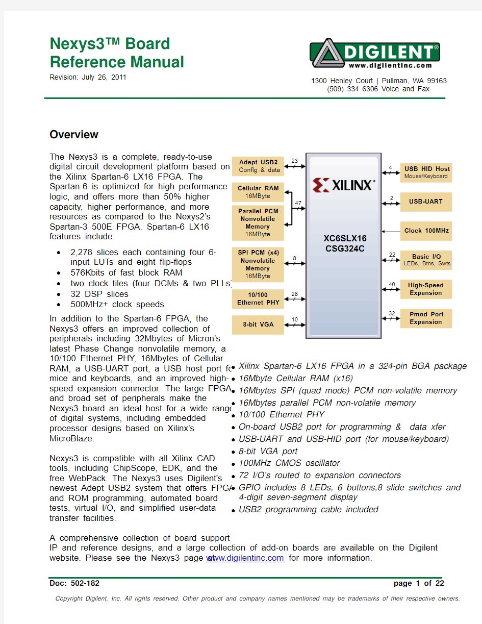
Overview Array The Nexys3 is a complete, ready-to-use
digital circuit development platform based on
the Xilinx Spartan-6 LX16 FPGA. The
Spartan-6 is optimized for high performance
logic, and offers more than 50% higher
capacity, higher performance, and more
resources as compared to the Nexys2’s
Spartan-3 500E FPGA. Spartan-6 LX16
features include:
?2,278 slices each containing four 6-
input LUTs and eight flip-flops
?576Kbits of fast block RAM
?two clock tiles (four DCMs & two PLLs)
?32 DSP slices
?500MHz+ clock speeds
In addition to the Spartan-6 FPGA, the
Nexys3 offers an improved collection of
peripherals including 32Mbytes of Micron’s
latest Phase Change nonvolatile memory, a
10/100 Ethernet PHY, 16Mbytes of Cellular
RAM, a USB-UART port, a USB host port for
mice and keyboards, and an improved high-
speed expansion connector. The large FPGA
and broad set of peripherals make the
Nexys3 board an ideal host for a wide range
of digital systems, including embedded
processor designs based on Xilinx’s
MicroBlaze.
Nexys3 is compatible with all Xilinx CAD
tools, including ChipScope, EDK, and the
free WebPack. The Nexys3 uses Digilent's
newest Adept USB2 system that offers FPGA
and ROM programming, automated board
tests, virtual I/O, and simplified user-data
transfer facilities.
A comprehensive collection of board support
IP and reference designs, and a large collection of add-on boards are available on the Digilent
website. Please see the Nexys3 page at https://www.doczj.com/doc/9b13426657.html, for more information.
Configuration
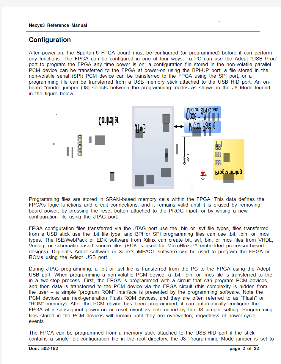
After power-on, the Spartan-6 FPGA board must be configured (or programmed) before it can perform any functions. The FPGA can be configured in one of four ways: a PC can use the Adept "USB Prog" port to program the FPGA any time power is on; a configuration file stored in the non-volatile parallel PCM device can be transferred to the FPGA at power-on using the BPI-UP port; a file stored in the non-volatile serial (SPI) PCM device can be transferred to the FPGA using the SPI port; or a programming file can be transferred from a USB memory stick attached to the USB HID port. An on-board "mode" jumper (J8) selects between the programming modes as shown in the J8 Mode legend in the figure below.
Programming files are stored in SRAM-based memory cells within the FPGA. This data defines the FPGA’s logic functions and circuit connections, and it remains valid until it is erased by removing board power, by pressing the reset button attached to the PROG input, or by writing a new configuration file using the JTAG port.
FPGA configuration files transferred via the JTAG port use the .bin or .svf file types, files transferred from a USB stick use the .bit file type, and BPI or SPI programming files can use .bit, .bin, or .mcs types. The ISE/WebPack or EDK software from Xilinx can create bit, svf, bin, or mcs files from VHDL, Verilog, or schematic-based source files (EDK is used for MicroBlaze? embedded processor-based designs). Digilent's Adept software or Xilinx's iMPACT software can be used to program the FPGA or ROMs using the Adept USB port.
During JTAG programming, a .bit or .svf file is transferred from the PC to the FPGA using the Adept USB port. When programming a non-volatile PCM device, a .bit, .bin, or .mcs file is transferred to the in a two-step process. First, the FPGA is programmed with a circuit that can program PCM devices, and then data is transferred to the PCM device via the FPGA circuit (this complexity is hidden from the user – a simple “program ROM” interface is presented by the programming software. Note the PCM devices are next-generation Flash ROM devices, and they are often referred to as "Flash" or "ROM" memory). After the PCM device has been programmed, it can automatically configure the FPGA at a subsequent power-on or reset event as determined by the J8 jumper setting. Programming files stored in the PCM devices will remain until they are overwritten, regardless of power-cycle events.
The FPGA can be programmed from a memory stick attached to the USB-HID port if the stick
JTAG (both jumpers loaded), and board power is cycled. The FPGA will automatically reject any .bit files that are not built for the proper FPGA.
After being successfully programmed, the FPGA will cause the "Done" LED to illuminate. Pressing the Reset button at any time will reset the configuration memory in the FPGA. After being reset, the
FPGA will immediately attempt to reprogram itself from one of the PCM devices if the J8 Mode jumper is set to BPI or SPI mode.
Adept
Power
Switch Power Jack
Power Reset Power Select LEDs Slide switches Push buttons
7-seg USB 10/100Pmod
VHDC Conncector
Digilent's Adept software offers a simplified programming interface and many additional features as described below. The Adept USB port is fully compatible with all Xilinx tools, including the iMPACT programming software. The Adept features are always available, regardless of how the FPGA was programmed.
Adept System
Digilent's Adept high-speed USB2 system can be used to program the FPGA and PCM devices, run automated board tests, add PC-based virtual I/O devices (like buttons, switches, and LEDs) to FPGA designs, and exchange register-based and file-based data with the FPGA. Adept automatically recognizes the Nexys3 board and presents a graphical interface with tabs for each of these applications. Adept also includes public APIs/DLLs so that users can write applications to exchange data with the Nexys3 board at up to 38Mbytes/sec. The Adept application, an SDK, and reference materials are freely downloadable from the Digilent website.
To program the Nexys3 board using Adept, first
set up the board and initialize the software:
?plug in and attach the power supply
?plug in the USB cable to the PC and to
the USB port on the board
?start the Adept software
?turn ON Nexys3's power switch
?wait for the FPGA to be recognized.
Use the browse function to associate the
desired .bit file with the FPGA, and click on the
Program button. The configuration file will be
sent to the FPGA, and a dialog box will indicate
whether programming was successful. The
configuration “done” LED will light after the
FPGA has been successfully configured.
Before starting the programming sequence, Adept ensures that any selected configuration file
contains the correct FPGA ID code – this prevents incorrect .bit files from being sent to the FPGA.
In addition to the navigation bar and browse and program buttons, the Config interface provides an
Initialize Chain button, console window, and status bar. The Initialize Chain button is useful if USB communications with the board have been interrupted. The console window displays current status, and the status bar shows real-time progress when downloading a configuration file.
Memory Interface
The Memory tab allows .bin, .bit, and .mcs
configuration files to be transferred to the on-
board BPI (parallel) or SPI (serial) PCM devices
for subsequent FPGA programming, and allows
user data files to be transferred to/from the
PCM devices or RAM memories at user-
specified addresses. The target memory is
selected by clicking one of the three radio
buttons in the upper-right corner.
All three memory devices (the PCM's and the cellular RAM) can be fully tested by clicking the Full Test button. They can also be completely erased by clicking the Erase button.
The Read/Write tools allow data to be
exchanged between files on the host PC and specified address ranges in the memory devices.
Test Interface Array The test interface provides an easy way to verify many of the board's hardware circuits and interfaces. These are divided into two major categories: on-board memory (RAM and Flash) and peripherals. In both cases, the FPGA is configured with test and PC-communication circuits, overwriting any FPGA configuration that may have been present.
Clicking the Run RAM/Flash Test button will identify the CellularRam, SPI Flash, and BPI Flash memory by reading out and verifying the IDCODE on each memory. The memory contents will not be modified. To run a full test on a particular memory device, refer to the Full Test in the Memory Tab.
Clicking the Start Peripherals Test button will initialize GPIO and user I/O testing. Once the indicator near the Start Peripherals Test button turns green, all peripheral tests can be run.
The Test Shorts feature checks all discrete
I/O’s for shorts to Vdd, GND, and neighboring I/O pins. The switches and buttons graphics
show the current states of those devices on the
Nexys3 board. Connect a VGA monitor and USB mouse to visually test the J2 VGA port and J4 USB port respectively.
Register I/O Array The register I/O tab requires that a corresponding IP block, available in the Parallel Interface reference design (DpimRef.vhd) on the Adept page of the Digilent website, is included and active in the FPGA. This IP block provides an EPP-style interface, where an 8-bit address selects a register, and data read and write buttons transfer data to and from the selected address. Addresses entered into the address field must match the physical address included in the FPGA IP block.
Register I/O provides an easy way to move
small amounts of data into and out of specific
registers in a given design. This feature greatly simplifies passing control parameters into a design, or reading low-frequency status information out of a design.
File I/O Array The File I/O tab can transfer files between the PC and the Nexys3 FPGA. A number of bytes (specified by the Length value) can be streamed into a specified register address from a file or out of a specified register address into a file. During upload and download, the file start location can be specified in terms of bytes.
As with the Register I/O tab, File I/O also
requires specific IP to be available in the
FPGA. This IP can include a memory controller for writing files into the on-board Ram and Flash memories.
The I/O Expand tab works with an IP block in
the FPGA to provide additional simple I/O
beyond the physical devices found on the
Nexys3 board. Virtual I/O devices include a 24-
LED light bar, 16 slide switches, 16 push
buttons, 8 discrete LEDs, a 32-bit register that
can be sent to the FPGA, and a 32-bit register
that can be read from the FPGA. The IP block,
available in the Adept I/O Expansion reference
design (AdeptIOExpansion.zip) on the Adept
page of the Digilent website, provides a simple
interface with well-defined signals. This IP
block can easily be included in, and accessed
from, user-defined circuits.
For more information, see the Adept
documentation available at the Digilent
website.
Power Supplies
The Nexys3 board can receive power from the Adept USB port or from an external power supply. Jumper JP1 (near the power jack) determines which source is used.
The USB port can deliver enough power for the vast majority of designs. It is possible that a very demanding application, including an application that drives many peripheral boards, might require more power than can be delivered by the USB port. Some applications may also need to run without being connected to a PC’s USB port. In either case, an external power supply or battery pack can be used by setting JP1 to “Wall”.
The main regulator on the Nexys3 can accommodate input voltages up to 15VDC. An external DC wall-plug supply should provide at least five watts of input power, and use a coax center-positive
2.1mm internal-diameter plug. An external battery pack can also be used by connecting the battery’s terminal leads to connector J11 (J11 is in parallel with the wall-plug power jack, so if a battery pack is connected, a wall plug should not be). An external battery pack should be limited to 12VDC, and should be capable of delivering adequate power for the application.
Voltage regulator circuits from Linear Technology create the required 3.3V, 2.5V, 1.8V, and 1.2V supplies from the main power input. The table below provides additional information (typical currents depend strongly on FPGA configuration and the values provided are typical of medium size/speed designs).
The Nexys3 power supplies are enabled (or turned on) by a logic-level Power switch (SW8). A power-good LED (LD8), driven by the wired-OR of the “power good” outputs on the supplies, indicates that all supplies are operating within 10% of nominal.
The VU output of the main power jumper (JP1) is available to the VHDC expansion connector if
jumper JP4 is loaded. Care must be taken to ensure the VUEXP delivered to any attached expansion board is the correct voltage – since VU is driven directly from an attached supply, this means a supply of the proper voltage must be used (e.g., 5V).
Memory
The Nexys3 board contains three external memories, all from Micron: a 128Mbit Cellular RAM
(pseudo-static DRAM); a 128Mbit parallel non-volatile PCM (phase-change memory); and a 128Mbit serial PCM device. The Cellular RAM and parallel PCM device share a common bus, and the serial PCM is on a dedicated quad-mode (x4) SPI bus. The non-volatile PCM memories are byte and bit alterable without requiring a block erase, so they are faster and more versatile than conventional Flash in most applications. Reference designs available on the Digilent website show examples of using the Cellular RAM in asynchronous and synchronous modes, as well as examples of reading and writing both PCM devices.
Nexys3 Power Supplies
Supply Circuits
Device Amps (max/typ) 3.3V FPGA I/O, USB ports, Clocks, ROM & RAM I/O, Ethernet IC13: LTC3633 3A / 200mA 2.5V Optional voltage for Bank0 and VHDC connector IC14: LTC3619 800mA / 0mA 1.2V FPGA Core
IC13: LTC3633 3A / 0.2 to 1.0A 1.8V RAM and ROM core
IC14: LTC3619
400mA / 0.1 to 0.3A
The 16Mbyte Cellular RAM (Micron part number M45W8MW16) has a 16-bit bus that supports 8 or 16 bit data access. It can operate as a typical asynchronous SRAM with read and write cycle times of
70ns, or as a synchronous memory with an 80MHz bus. When operated as an asynchronous SRAM, the Cellular RAM automatically refreshes its internal DRAM arrays, allowing for a simplified memory controller (similar to any SRAM controller). When operated in synchronous mode, continuous transfers of up to 80MHz are possible.
The parallel PCM device (Micron part number NP8P128A13T1760E) is organized as 8Mwords of
16bits each. It contains 128 individually erasable 64K-blocks, one of which is subdivided into four 16K “parameter blocks” that can offer increased data protection. Normally, a device with a parameter block at the high end of the address space is loaded (a “top parameter” block device). The parallel PCM memory offers 115ns read cycle times, with 25ns page-mode reads within blocks. It has an internal 64-byte write buffer that can be written with 50ns cycle times, and the 64-byte buffer can be transferred to the Flash array in 120us (typical). The parallel PCM device also contains an SPI port for serial data transfer, but that function is not enabled on the Nexys3 board (the ADV and WAIT signals are connected between the FPGA and PCM, but they serve no functions).
The Cellular RAM and parallel PCM share a common 16-bit data bus and 24-bit address bus. The Cellular RAM is byte addressable using the upper-byte and lower-byte signals (MT-UB and MT-LB), but the P8P PCM is configured for 16 byte operations only (it is not byte addressable). The output enable (OE) and write enable (WE) signals are shared by both devices, but each device has individual chip enable (CE) signals. Additionally, the Cellular RAM has clock (MT-CLK), wait (MT-WAIT), address valid (MT-ADV) and control register enable (MT_CRE) signals available to the FPGA for use with synchronous transfers, and the PCM device has Reset (RP#). With simple changes, the Nexys3 board can accommodate either the PCM device or the older “P33” Flash device. The signal names in the Nexys3 schematic reference the P33 device; the P33 ADV and WAIT signals are not used in by the PCM device.
The 16Mbyte serial PCM device (Micron part number NP5Q128A13ESFC0E) is also bit alterable without requiring an erase cycle. It supports the legacy SPI protocol as well as the newer Quad I/O and Dual I/O protocols, at bus speeds up to 50MHz.
FPGA configuration files can be written to both PCM devices, and mode settings are available to cause the FPGA to automatically read a configuration from one of these devices at power on. A Spartan-6 LX16 configuration file requires about 512Kbytes of memory, leaving about 97% of the PCM devices available for user data.
Both PCM devices are loaded with configuration files at the factory. The SPI PCM device contains a file that configures the FPGA to test the Nexys3 memory devices during manufacturing, and this file isn’t needed after the board test is complete. The BPI PCM device contains a file that configures the Nexys3 with a basic user demonstration program, and it can be used to verify board functions. This same .bit file (and complete project) is available for download from the Digilent website. If Mode jumper J8 is set to BPI mode and power is applied, the user demo configuration will be loaded. The demo drives a counter on the 7-segment display, drives the user LEDs on and off when the user switches are toggled, turns off digits on the 7-segment display when user buttons are pressed, and drives an image out the VGA port. A USB mouse can be connected to J4 for a simple visual demonstration.
Please refer to the manufacturer’s data sheets and the reference designs posted on Digilent’s website for more information about the memory devices.
Ethernet PHY
The Nexys3 board includes an SMSC 10/100 Ethernet PHY (SMSC part number LAN8710) paired with an RJ-45 Ethernet jack with integrated magnetics. EDK-based designs can access the PHY using either the xps_ethernetlite IP core or the xps_ll_temac IP core. The Nexys3 Base System Builder (BSB) support package automatically generates a test application for the Ethernet MAC; this can be used as a reference for creating custom designs. ISE designs can use the IP Core Generator wizard to create an Ethernet MAC controller IP core. The SMSC PHY uses the MII interface and supports 10/100 Mb/s. At power-on reset, the PHY is set to the following defaults:
?MII mode interface
?100Base-TX with auto negotiation enabled, advertising half-duplex, with CRS active during receive
?PHY address = 000
Refer to the LAN8710A data sheet on the https://www.doczj.com/doc/9b13426657.html, website for further information.
SMSC LAN8710A
Oscillators/Clocks
The Nexys3 board includes a single 100MHz CMOS oscillator connected to pin V10 (V10 is the GCLK0 input in bank 2). The input clock can drive any or all of the four clock management tiles in the
automatically be rejected. Note the PIC24 reads the FPGA's mode, init, and done pins, and can drive the PROG pin as a part of the programming sequence.
HID Controller
To access the USB host controller, EDK designs
can use the standard PS/2 core (non-EDK designs
can use a simple state machine). Reference
designs posted on the Digilent website show an
example of reading characters from a USB
keyboard connected to the USB host interface.
Mice and keyboards that use the PS/2 protocol
use a two-wire serial bus (clock and data) to
communicate with a host device. Both use 11-bit
words that include a start, stop, and odd parity bit,
but the data packets are organized differently, and
the keyboard interface allows bi-directional data transfers (so the host device can illuminate state LEDs on the keyboard). Bus timings are shown in the figure. The clock and data signals are only driven when data transfers occur, and otherwise they are held in the idle state at logic ‘1’. The timings define signal requirements for mouse-to-host communications and bi-directional keyboard communications. A PS/2 interface circuit can be implemented in the FPGA to create a keyboard or mouse interface.
Keyboard
The keyboard uses open-collector drivers so the keyboard, or an attached host device, can drive the two-wire bus (if the host device will not send data to the keyboard, then the host can use input-only ports).
PS/2-style keyboards use scan codes to communicate key press data. Each key is assigned a code that is sent whenever the key is pressed. If the key is held down, the scan code will be sent repeatedly about once every 100ms. When a key is released, an F0 key-up code is sent, followed by the scan code of the released key. If a key can be shifted to produce a new character (like a capital letter), then a shift character is sent in addition to the scan code, and the host must determine which ASCII character to use. Some keys, called extended keys, send an E0 ahead of the scan code (and they may send more than one scan code). When an extended key is released, an E0 F0 key-up code is sent, followed by the scan code. Scan codes for most keys are shown in the figure. A host device can also send data to the keyboard. Below is a short list of some common commands a host might send.
ED Set Num Lock, Caps Lock, and Scroll Lock LEDs. Keyboard returns FA after receiving ED, then host sends a byte to set LED status: bit 0 sets Scroll Lock, bit 1 sets Num Lock, and bit 2 sets Caps lock. Bits 3 to 7 are ignored.
EE Echo (test). Keyboard returns EE after receiving EE.
F3 Set scan code repeat rate. Keyboard returns F3 on receiving FA, then host sends second byte to set the repeat rate.
FE Resend. FE directs keyboard to re-send most recent scan code.
FF Reset. Resets the keyboard.
The keyboard can send data to the host only when both the data and clock lines are high (or idle). Since the host is the bus master, the keyboard must check to see whether the host is sending data before driving the bus. To facilitate this, the clock line is used as a “clear to send” signal. If the host pulls the clock line low, the keyboard must not send any data until the clock is released. The keyboard sends data to the host in 11-bit words that contain a ‘0’ start bit, followed by 8-bits of scan code (LSB first), followed by an odd parity bit and terminated with a ‘1’ stop bit. The keyboard generates 11 clock transitions (at 20 to 30KHz) when the data is sent, and data is valid on the falling edge of the clock. Scan codes for most PS/2 keys are shown in the figure below.
Mouse
The mouse outputs a clock and data signal when it is moved, otherwise, these signals remain at logic ‘1’. Each time the mouse is moved, three 11-bit words are sent from the mouse to the host device. Each of the 11-bit words contains a ‘0’ start bit, followed by 8 bits of data (LSB first), followed by an odd parity bit, and terminated with a ‘1’ stop bit. Thus, each data transmission contains 33 bits, where bits 0, 11, and 22 are ‘0’ start bits, and bits 11, 21, and 33 are ‘1’ stop bits. The three 8-bit data fields contain movement data as shown in the figure above. Data is valid at the falling edge of the clock, and the clock period is 20 to 30KHz.
The mouse assumes a relative coordinate system wherein moving the mouse to the right generates a positive number in the X field, and moving to the left generates a negative number. Likewise, moving the mouse up generates a positive number in the Y field, and moving down represents a negative number (the XS and YS bits in the status byte are the sign bits – a ‘1’ indicates a negative number). The magnitude of the X and Y numbers represent the rate of mouse movement – the larger the number, the faster the mouse is moving (the XV and YV bits in the status byte are movement overflow indicators – a ‘1’ means overflow has occurred). If the mouse moves continuously, the 33-bit transmissions are repeated every 50ms or so. The L and R fields in the status byte indicate Left and Right button presses (a ‘1’ indicates the button is being pressed).
VGA Port
The Nexys3 board uses 10 FPGA signals to create a VGA port with 8-bit color and the two standard sync signals (HS – Horizontal Sync, and VS – Vertical Sync). The color signals use resistor-divider circuits that work in conjunction with the 75-ohm termination resistance of the VGA display to create eight signal levels on the red and green VGA signals, and four on blue (the human eye is less sensitive to blue levels). This circuit, shown in figure 13, produces video color signals that proceed in equal increments between 0V (fully off) and 0.7V (fully on). Using this circuit, 256 different colors can be
displayed, one for each unique 8-bit pattern. A video controller circuit must be created in the FPGA to drive the sync and color signals with the correct timing in order to produce a working display system.
VGA System Timing
VGA signal timings are specified, published, copyrighted and sold by the VESA organization (https://www.doczj.com/doc/9b13426657.html,). The following VGA system timing information is provided as an example of how a VGA monitor might be driven in 640 by 480 mode. For more precise information, or for
information on other VGA frequencies, refer to documentation available at the VESA website.
CRT-based VGA displays use amplitude-modulated moving electron beams (or cathode rays) to display information on a phosphor-coated screen. LCD displays use an array of switches that can impose a voltage across a small amount of liquid crystal, thereby changing light permittivity through the crystal on a pixel-by-pixel basis. Although the following description is limited to CRT displays, LCD displays have evolved to use the same signal timings as CRT displays (so the “signals” discussion below pertains to both CRTs and LCDs). Color CRT displays use three electron beams (one for red, one for blue, and one for green) to energize the phosphor that coats the inner side of the display end of a cathode ray tube (see illustration). Electron beams emanate from “electron guns” which are finely-pointed heated cathodes placed in close proximity to a positively charged annular plate called a “grid”. The electrostatic force imposed by the grid pulls rays of energized electrons from the cathodes, and
Mouse Data Format
accelerated towards the grid, but they soon fall under the influence of the much larger
electrostatic force that results from the entire
phosphor-coated display surface of the CRT being charged to 20kV (or more). The rays are focused to a fine beam as they pass
through the center of the grids, and then they accelerate to impact on the phosphor-coated
display surface. The phosphor surface glows
brightly at the impact point, and it continues
to glow for several hundred microseconds after the beam is removed. The larger the current fed into the cathode, the brighter the
phosphor will glow. Between the grid and the display surface, the beam passes through the neck of the CRT
where two coils of wire produce orthogonal electromagnetic fields. Because cathode rays are
composed of charged particles (electrons), they can be deflected by these magnetic fields. Current waveforms are passed through the coils to produce magnetic fields that interact with the cathode rays and cause them to transverse the display surface in a “raster” pattern, horizontally from left to right and vertically from top to bottom. As the cathode ray moves over the surface of the display, the current sent to the electron guns can be increased or decreased to change the brightness of the display at the cathode ray impact point.
Information is only displayed when the beam is moving in the “forward” direction (left to right and top Display Surface 640 pixels per row are displayed
during forward beam trace pixel 0,639pixel 0,0pixel 479,0pixel 479,639High voltage Deflection coils Grid Electron guns
(Red, Blue, Green)gun grid deflection Cathode ray tube Cathode ray
horizontal passes the cathode makes over the display area, and a number of “columns” that corresponds to an area on each row that is assigned to one “picture element” or pixel. Typical displays use from 240 to 1200 rows and from 320 to 1600 columns. The overall size of a display and the number of rows and columns determines the size of each pixel.
Video data typically comes from a video refresh memory, with one or more bytes assigned to each pixel location (the Nexys3 uses three bits per pixel). The controller must index into video memory as the beams move across the display, and retrieve and apply video data to the display at precisely the time the electron beam is moving across a given pixel.
HS and VS timings signals and coordinate
the delivery of video data based on the pixel
clock. The pixel clock defines the time
available to display one pixel of information.
The VS signal defines the “refresh”
frequency of the display, or the frequency at
which all information on the display is
redrawn. The minimum refresh frequency is
a function of the display’s phosphor and
electron beam intensity, with practical
refresh frequencies falling in the 50Hz to
120Hz range. The number of lines to be
displayed at a given refresh frequency
defines the horizontal “retrace” frequency.
For a 640-pixel by 480-row display using a
25MHz pixel clock and 60 +/-1Hz refresh,
the signal timings shown in the table at right can be derived. Timings for sync pulse width and front and back porch intervals (porch intervals are the pre- and post-sync pulse times during which information cannot be displayed) are based on observations taken from actual VGA displays.
A VGA controller circuit decodes the output of a horizontal-sync counter driven by the pixel clock to generate HS signal timings. This counter can be used to locate any pixel location on a given row. Likewise, the output of a vertical-sync counter that increments with each HS pulse can be used to generate VS signal timings, and this counter can be used to locate any given row. These two continually running counters can be used to form an address into video RAM. No time relationship between the onset of the HS pulse and the onset of the VS pulse is specified, so the designer can arrange the counters to easily form video RAM addresses, or to minimize decoding logic for sync
pulse generation.
Basic I/O
The Nexys3 board includes eight slide switches, eight push buttons, eight individual LEDs, and a four digit seven-segment display. The pushbuttons and slide switches are connected to the FPGA via series resistors to prevent damage from inadvertent short circuits (a short circuit could occur if an FPGA pin assigned to a pushbutton or slide switch was inadvertently defined as an output). The pushbuttons are "momentary" switches that normally generate a low output when they are at rest, and a high output only when they are pressed. Slide switches generate constant high or low inputs depending on their position.
The eight individual high-efficiency LEDs are anode-connected to the FPGA via 390-ohm resistors, so they will turn on when a logic high voltage is applied to their respective I/O pin. Additional LEDs that are not user-accessible indicate power-on, FPGA programming status, and USB and Ethernet port status.
Seven-Segment Display
The Nexys3 board contains a four-digit common anode seven-segment LED display. Each of the four digits is composed of seven segments arranged in a “figure 8” pattern, with an LED embedded in each segment. Segment LEDs can be individually illuminated, so any one of 128 patterns can be displayed on a digit by illuminating certain LED segments and leaving the others dark. Of these 128 possible patterns, the ten corresponding to the decimal digits are the most useful.
The anodes of the seven LEDs forming each digit are tied together into one “common anode” circuit node, but the LED cathodes remain separate. The common anode signals are available as four “digit enable” input signals to the 4-digit display. The cathodes of similar segments on all four displays are connected into seven circuit nodes labeled CA through CG (so, for example, the four “D” cathodes from the four digits are grouped together into a single circuit node called “CD”). These seven cathode signals are available as inputs to the 4-digit display. This signal connection scheme creates a
multiplexed display, where the cathode signals are common to all digits but they can only illuminate the segments of the digit whose corresponding anode signal is asserted.
A scanning display controller circuit can be used to show a four-digit number on this display. This circuit drives the anode signals and corresponding cathode patterns of each digit in a repeating, continuous succession, at an update rate that is faster than the human eye can detect. Each digit is illuminated just one-quarter of the time, but because the eye cannot perceive the darkening of a digit before it is illuminated again, the digit appears continuously illuminated. If the update or “refresh” rate is slowed to around 45 hertz, most people will begin to see the display flicker.
In order for each of the four digits to appear bright and continuously illuminated, all four digits should be driven once every 1 to 16ms, for a refresh frequency of 1KHz to 60Hz. For example, in a 60Hz refresh scheme, the entire display would be refreshed once every 16ms, and each digit would be illuminated for ? of the refresh cycle, or 4ms. The controller must drive the cathodes with the correct pattern when the
corresponding anode signal is driven.
To illustrate the process, if AN0 is asserted while CB and CC are
asserted, then a “1” will be displayed
in digit position 1. Then, if AN1 is
asserted, then a “7” will be displayed in digit position 2. If AN0 and CB, CC are driven for 4ms, and then A1 and CA, CB, CC are driven for 4ms in an endless succession, the display will show “17” in the first two digits. An example timing diagram for a four-digit controller is provided.
Expansion Connectors
The Nexys3 board has a 68-pin VHDC connector for high-speed/parallel I/O, and an 8-pin Pmod connector for lower speed and lower pin-count I/O.
VHDC Connector
The VHDC connector includes 40 data signals (routed as 20 impedance-controlled matched pairs), 20 grounds (one per pair), and eight power signals. This connector, commonly used for SCSI-3 applications, can accommodate data rates of several hundred megahertz on every pin. Both board-to-board and board-to-cable mating connectors are available. Data sheets for the VHDC connector and for mating board and cable connectors can be found on the Digilent website, as well as on other vendor and distributor websites. Mating connectors and cables of various lengths are also available from Digilent and from distributors.
All FPGA pins routed to the VHDC connector are located in FPGA I/O bank0. The FPGA's bank0 I/O power supply pins and the VHDC connector's four Vcc pins are connected together by a small, segregated power supply plane in the PCB. This sub-plane can be connected to 2.5V or 3.3V, depending on the position of jumper JP8. This arrangement allows peripheral boards and the FPGA to share the same Vcc and signaling voltage across the connector, whether it be 3.3V or 2.5V.
The unregulated board voltage VU5V0 (nominally 5V) is also routed to four other VHDC pins, supplying up to 1A of additional current to peripheral boards. A second jumper (JP4) allows the unregulated board voltage to be disconnected
from the VHDC connector if desired.
All I/O’s to the VHDC connector are routed as
matched pairs to support LVDS signaling,
commonly powered at 2.5V. The connector
uses a symmetrical pinout (as reflected around
the connector's vertical axis) so that peripheral
boards as well as other system boards can be
connected. Connector pins 15 and 49 are
routed to FPGA clock input pins.
车间管理手册 目录 第一章排产制度 (2) 第二章排产控制程序 (2) 第三章品质制度 (2) 第四章品质控制程序 (3) 第五章物料制度 (3) 第六章物料控制程序 (3) 第七章车间人事管理制度 (4) 第八章车间整洁制度 (4) 第九章整洁制度控制程序 (5) 第十章车间安全生产控制 (5) 第十一章管理者责任及工作态度 (5) 第十二章管理人员应该具备的九项能力 (6) 第十三章如何做好合格的管理者 (6)
第一章排产制度 1. 首先是勇于接受上级的安排,积极参与,认真组织下层策划按时按质完成排产的方法和步骤,做 到胸有成竹,每天自觉地掌握排产计划,并切实施地分析排产完成情况,控制生产的进度。 2. 主动地将完成排产的不利因素与有关部门负责人沟通,争取他们的有力支持协助,力尽人际关系 去解决完成排产的方法,物料、人力、机械、工具及其他方面的配合。 3. 采取有效的措施,做好突变的调整工作,及时分析本周排产的物料供应情况,努力使自己应付自 如,群策群力,团结一致,排除一切影响完成生产任务的隐患。 4. 坚持科学管理,发挥统筹之作用,使每天的生产任务都在控制当中,做到发现问题要快,判断问 题要准,解决问题方法要对,行动要迅速,及时上下沟通部门沟通,令自己的工作达到大家的共识与同步,想方设法激励员工的士气,推动改善和进步。 5. 不断地结合实际分析,做好生产衔接与平衡,尤其是新产品更要保持每天的平衡与调整防止浪费 工时,使生产力发挥的更佳。对一些变化属不可抗拒的条件,应懂得应付,某些条件不具备的排产,要及时提请生产办更改,尽一切的努力克服人为的甩产。 6. 班组长要做好交接班工作,保持机器的完好整洁交班,如机器或工具有问题,应当面与接班的班 组长交代,尽量避免浪费工时,力求工作平衡、顺利。 7. 新产品投产,工艺人员应全力协助,将方法,技术逐一工序反复辅导,令工人完全掌握,并操作 自如,直至QC一天内无退货。班组长要自始自终与技术组人员携手合作,逐一跟进及品质的检查,确保新产品的质量要求合格直至完全理解和掌握每道工序的方法和技术及质量控制等。 8. 各生产线如遇牌产不足或生产效率高而导致缩短工作时间的(即提早下班),管理人员应从分利 用空余时间对工人进行培训,使工人能掌握多面的生产工艺,做到人尽其才,发挥更好。 第二章排产控制程序 1.配合公司,根据生产部下达的生产任务指标,结合本部的生产实力,具体组织生产计划的实施工作。 2.负责实施上级下达的生产任务指标,贯彻落实致员工。 3.制定和执行现场作业标准及工艺流程,从而使生产的产品,按照客户的需要进行,保证进度和质 量。 4.实现全面均衡有节奏的同步生产,使最终的生产便于包装及装箱。 第三章品质制度 1. 认真了解自己负责的产品样板及标准的要求,做到心中有数,对极限的标准也应理解。 2. 与工艺的有关人员同心协力,共同探讨和研究产品每一道工序的品质控制,务求使每一个生产线 的工人懂方法、会操作、能控制,使质量在每一环都能得到控制。 3. 做好产品在投放前的准备工作,在开始生产新产品前要严阵以待,密切注释成品的每到工序所引 致品质上的问题,并能及时寻找解决的方法,主动联络有关人员的协助,直到弄清情况,完全解决,以保证产品的优质。 4. 经常性地分析人,机(工具)及物料所导致的品质问题,做到方向明,判断准,行动快的去解决 造成品质不良的所在,排除一切阻力,尽最大的努力,实现产品的标准要求。 5. 严格执行品质制度,主动并自觉的配合QC的控制工作。坚持每小时的自我质量巡查,发现问题 及时解决,如有困难,应立即报告上一级协助解决。 6. 对QC要求返工要立即反应,清楚了解返工的原因做好总结分析,吸取教训,寻求方法改善,重 新整顿安排生产,确保产品质量,并马上组织返工或拣货。 7. 保持每天定时抽查成品,从成品中自我鉴定,发现成品中有质量上缺点时,要立即抽查出差的原 因及工序,直到解决问题为止,坚持不懈,效果是会始终如一的。 8. 班组长必须辅导工人不偏不移地按工程部订立的方法去做,如发现退货应及时知会工程技术部和
国外主要医用敷料生产厂商竞争力分析 由于传统医用敷料产品难以满足慢性和复杂伤口的治疗需求,今后高端敷料将成为推动敷料市场发展的主要驱动力。预计2017年,全球高端医用敷料销售收入将达到160亿美元。目前在我国医用敷料产品中,高端新型敷料生产方面较为薄弱,主要依靠进口。此次选出5家国外主要医用敷料生产厂商,对它们从技术水平以及销售状况等方面进行解析,我们的企业可以在此基础上客观反思自身发展,正所谓知己知彼方能百战百胜。 1、美国3M公司五年研发累计达70.69亿美元 3M公司全称是明尼苏达矿务及制造业公司(Minnesota Mining and Manufacturing Corporation),是全球产品多元化的跨国公司,涉及范围:办公用品、标识、电信通讯、医疗用品、货物运输、安保与防护。医疗主要涉及口腔、高端医用辅料、听诊器。 技术水平 3M为全球性的多元化科技企业,国际公认的研发领域的先驱。公司生产了数以万计的创新产品,在医疗产品、高速公路安全、办公文教产品、光学产品等核心市场占据领导地位。2011年3M公司研发投入高达15.7亿美元,过去五年的研发累计高达70.69亿美元。 销售状况 2011年全年,3M年销售额达296亿美元,同比上涨11.1%。公司六大事业部中除显示与标示业务亏损外,销售均呈现增长态势,其中工业运输业务部业务增长达19.5%,安保及防护业务增长达15.2%。医疗产品业务、文教及家庭用品业务、电子电力及通讯业务三大事业中心均与2010年持平。拉美、加拿大地区2011年实现销售增长15.6%,成为3M业务中增长最迅速的地区。2011全年公司实现每股收益5.96美元,增长5.9%;运营利润实现20.9%的增长,投资资本回报率达19.9%。 2、瑞典Molnlycke Health Care公司年销售额近8亿欧元 瑞典墨尼克医疗用品有限公司(M?lnlycke Health Care)是一家全球领先的
公司制度 公司架构及职能范围 各部门岗位职责 公司管理制度和绩效考核 人员管理和招聘 公司保密条款
第一章公司部门职能范围公司架构 财务部会计出纳 营销部 国内业务 国际业务 行政部 人力资源 采购 总经理 董事会
电子商务售后服务物流仓库 市场部行政管理
第二章各部门岗位职责 一、行政部 行政部作为公司的一个职能部门,主要负责公司的行政管理、人力资源管理及营销中心办公事务管理;目前兼负责物流,仓储。 行政管理:负责公司的行政管理工作,包括制度管理、文档管理、考勤纪律、办公支持和公关接待等事宜。 人力资源管理:负责公司的人力资源管理工作,包括绩效考评、薪酬计核、职位管理、人事调整、员工档案管理、员工招聘、培训和员工关怀等事宜。 公司办公事务管理:负责公司的办公事务管理,如办公用品的管理和各种工作会议的组织工作等。具体职责如下: 1、拟定或协助拟定公司的各项经营管理制度; 2、起草或协助起草公司经营管理活动中需要的各种文件; 3、负责行政公文的签收、登记、流转、归档及业务文件的整理、归档; 4、协调解决各部门在经营管理活动中遇到的问题; 5、组织安排行政及其他会务,协调接待工作;
6、负责公司对外宣传及联系工作,管理公司网站; 7、负责公司文件、信函的发送、接收工作; 8、负责公司行政公章的保管、使用及各类文件的缮印; 10、负责公司日常办公用品、宣传品、名片的定制、保管、发放。 11、拟定公司人事、劳资等方面的规章制度; 12、拟定公司机构设置或调整方案; 13、负责公司员工的定岗定编工作; 14、负责公司员工的招聘工作; 15、拟定员工薪酬、福利等分配激励制度体系,并组织具体实施; 16、负责人力资源培训工作的组织与协调; 17、管理员工休假和考勤。 二、营销部: 1、营销部负责制定并推进实施全面的销售战略、销售方案,公司产品推广,业务渠道拓展,客 户开发,并对相关行业、市场进行前景分析及研究,制定市场营销方案,有效地管理客户。 具体职责如下: 1、协助总经理建立全面的销售战略; 2、制定并组织实施完整的销售方案; 3、与客户、同行业间建立良好的合作关系; 4、引导和控制市场销售工作的方向和进度; 5、组织部门开发多种销售手段,完成销售计划及回款任务; 6、管理销售人员,帮助建立、补充、发展、培养销售队伍;
安全生产责任制度 一、本企业安全机构设置 1)本企业设安全生产领导小组,由总经理任组长,由副总经理、生产厂长、 办公室主任、车间主任等人组成; 2)总经理为本企业安全生产第一责任人,各部门领导为本部门安全生产第 一责任人; 3)本企业设专职安全员一名; 二、总经理安全职责: 1)全面负责安全生产工作;建立、健全安全生产责任制; 2)督促、检查安全生产工作,及时消除生产安全事故隐患。 3)组织制定并实施生产安全事故应急救援预案; 4)及时、如实上级主管部门报告生产安全事故。 三、副总经理安全职责: 1)主管安全生产工作,定期听取汇报,及时解决安全生产中的重大问题; 2)组织制定《安全生产管理制度》和《操作规程》,并组织实施; 3)进行安全生产检查,落实重大事故隐患的整改; 4)组织各类重大事故和特大事故的调查处理; 5)负责制定劳动防护用品的分配和发放工作; 四、生产厂长安全职责: 1)对本企业生产安全技术问题全面负责; 2)负责安全技术研究工作,积极采用先进技术和安全防护装置,并落实重 大事故隐患的整改; 3)按照“三同时”原则在组织新、改、扩建项目时做到劳动、安全、卫生 设施与主体工程同时设计、同时施工、同时投入生产和使用; 4)参加各类重大事故的调查处理,采取有效措施防止事故重演。 五、办公室安全职责:
1)协助制定《安全生产管理制度》,并负责检查落实到位; 2)负责安全生产事故的统计、分析、存档等工作; 3)负责对临时来企业参观学习、办事人员进行入厂安全注意事项的宣传教 育工作; 4)协助搞好安全生产方针、政策、法规、制度等的宣传教育,提高职工的 安全意识; 六、生产科安全职责: 1)负责本企业的机械、电气、动力设备、工艺管道、通排风装置及工业建 筑物等的管理,使其符合安全技术要求; 2)组织对起重机械、施工机具、锅炉、压力容器及安全装置、热力管道、 采暖、通排风等设备的定期检查、检测工作; 3)负责制定和审查有关设备制造、改造、维护、检修的各项管理制度; 4)组织落实《安全生产管理制度》; 七、财务部门安全职责: 1)编制、平衡生产计划时,应保证安全技术措施资金的来源,确保“三同 时”的顺利实施; 2)监督安全技术措施、劳保用品、保健费用的开支情况,保证安全教育费 用的实际需要; 3)负责各类事故费用的支出,并纳入经济活动分析内容; 八、车间主任安全职责: 1)坚持“安全第一、预防为主”方针,认真贯彻执行党和国家的安全生产 法律、法规、标准; 2)对本部门员工(包括实习、代培人员)进行安全教育,并督促本部门员工 在生产穿戴劳动保护用品,并严格按照《操作规程》和《安全生产管理制度》生产; 3)发生事故时,立即组织抢救,保护好现场并立即报告有关部门,负责查 明事故原因和采取防范措施; 4)负责本部门所有生产设备、设施、工具的安全检查和保证其安全运行;
公司地址:北京市西城区宣武门西大街甲129号金隅大大厦1610室 1 宝获利公司、产品、服务及客户介绍 宝获利商用设备(北京)有限公司 2010年7月16日
公司地址:北京市西城区宣武门西大街甲129号金隅大大厦1610室 2 台湾振桦电子股份有限公司(POSIFLEX Corporation )是专业的设计、制造、销售POS 机及相关周边产品的上市公司,台湾股票代码:8114,在全球设有几十家分公司和分支机构,在大陆的分公司是宝获利商用设备(北京)有限公司。宝获利进入大陆已经12年。经过多年来的努力及成长,在POS 管理系统及相关周边产品设计制造领域中占有举足轻重的位置,并有多项设计领先于其他竞争厂商,今年的主题是洁净、节能、环保,宝获利为倡导环保、节能、低耗、减排做出很多贡献。 Headquarters 总公司POSIFLEX 位于台北五股工业区内,成立于1984年,注册资金美金一千七百万美金,总部现有员工235人。POSIFLEX 英文标识为振桦公司所生产POS 机的注册商标,为世界性注册商标,在全世界几十个国家都有注册,产品行销世界各地。宝获利为中文标识,取意为:“保您获利”,1998年在国内注册。POSIFLEX 产品在严格的品质要求下,从研发到制造皆于台湾总公司振桦电子股份有限公司(POSIFLEX Corporation )之研发室及工厂完成所有产品。所有系列产品皆通过CE 和FCC 的认证,生产工厂已取得国际品质认证 ISO 9001及环境认证 ISO 14001。POSIFLEX 一路领导着POS 管理系统之设计走向,申请的专利超过50多项,目前也尚有多项的专利案正在申请中。POSIFLEX 的产品结合了崭新的安全性、使用方便性的设计概念与巧思,是目前在POS 业界前所少见的。通过其全球驻外机构随时研究当今商业的发展方向,深谙商业客户对前台收款作业的要求,所有产品均体现出以人为本的设计理念,对细节方面的完美追求体现在所有POSIFLEX 产品之中。
FEATURES APPLICATIONS DESCRIPTION CC2590BLOCK DIAGRAM RF_P RXTX RF_N PAEN EN CC2590 https://www.doczj.com/doc/9b13426657.html,........................................................................................................................................................................................SWRS080–SEPTEMBER2008 2.4-GHz RF Front End,14-dBm output power ?All2.4-GHz ISM Band Systems ?Seamless Interface to2.4-GHz Low Power RF Devices from Texas Instruments?Wireless Sensor Networks ?Wireless Industrial Systems ?Up to+14-dBm(25mW)Output Power ?IEEE802.15.4and ZigBee Systems ?6-dB Typical Improved Sensitivity on CC24xx ?Wireless Consumer Systems and CC2500,CC2510,and CC2511 ?Wireless Audio Systems ?Few External Components –Integrated Switches –Integrated Matching Network CC2590is a cost-effective and high performance RF –Integrated Balun Front End for low-power and low-voltage 2.4-GHz –Integrated Inductors wireless applications. –Integrated PA CC2590is a range extender for all existing and future –Integrated LNA 2.4-GHz low-power RF transceivers,transmitters and ?Digital Control of LNA Gain by HGM Pin System-on-Chip products from Texas Instruments.?100-nA in Power Down(EN=PAEN=0)CC2590increases the link budget by providing a power amplifier for increased output power,and an ?Low Transmit Current Consumption LNA with low noise figure for improved receiver –22-mA at3-V for+12-dBm,PAE=23% sensitivity. ?Low Receive Current Consumption CC2590provides a small size,high output power RF – 3.4-mA for High Gain Mode design with its4x4-mm QFN-16package. – 1.8-mA for Low Gain Mode CC2590contains PA,LNA,switches,RF-matching,? 4.6-dB LNA Noise Figure,including T/R Switch and balun for simple design of high performance and external antenna match wireless applications. ?RoHS Compliant4×4-mm QFN-16Package ? 2.0-V to3.6-V Operation Please be aware that an important notice concerning availability,standard warranty,and use in critical applications of Texas Instruments semiconductor products and disclaimers thereto appears at the end of this data sheet.
经 营 管 理 制 度 市 场 篇 昆明圣川装饰工程有限公司 页脚内容1
业务部管理制度 第一部分业务部规章制度 1、业务部作为公司第一服务窗口,在外应注意言行举止,充分展现公司的形象。 2、业务部员工每天必须以饱满的精神上岗,以真诚、热情的服务对待每一位客户。 3、由业务部经理安排当天的工作任务,部门所有员工必须在规定时间内到达指定地 点,到达指定地点后应马上投入工作,杜绝拖拉现象。 4、见到客户应积极、主动上前,不得相互推让,攀谈时应注意客户的言行举止,及时了解 客户所需,并做详细记录。 5、与客户充分沟通,尽一切可能得到客户的信任,为其测房。 6、测房前应携带测房工具。(7米以上钢卷尺、速写本、测房记录表、正规笔记本。) 7、测房时要求数据准确,(如房间长宽高、梁、柱、门洞、窗洞、油烟机孔、下水道位置) 并用正规笔记本/客房登记表,记下客户对装修的要求、预投资金额、户型优缺点,以便做出相应的预算、设计。 页脚内容2
8、测房后应预约客户看预算的时间、地点。 9、测房当天应做出至少3份有价值的预算及平面布局图供客户参考。 10、客户对所提供方案略感兴趣,尽可能争取立即签合同;如客户还有待考虑或修改方案,在分别时要和客户约好下次再见面时间,为再拜访客户做好铺垫。 11、每天下班必须汇报当天工作情况及做好第二天的工作计划。 12、有事或生病须请假者3天以内写好请假条到部门经理处签字,四天以上到总经理处签字得到批准方可生效。 第二部分业务经理岗位职责 第二部分业务员岗位职责 第二部分业务部薪酬制度 一、业务部经理底薪:1500;(工程总造价) 1)保底任务15万的业绩;目标任务20万的业绩; 2)未达到保底任务每少1万,底薪下降100元,底薪最低不低于1000元;(无小组提成) 页脚内容3
互联网公司产品经理职责 职责一:市场调研 指积极的研究市场以便了解客户需求,竞争格局,和市场运作。最终目标则是发现机会,来创造新产品及改善现有产品。 通过以下方式来进行, 与客户或潜在客户交流 与直接面对客户的一线团队(如销售和支持)进行交流 研究市场分析报告和文章 体验竞争产品 持续跟踪客户行为 其它类似的手段 通过市场调研,产品经理最终会准备好商业案例,产品战略和商业需求文档(BRD),来描述如何利用潜在的市场机会。 职责二:产品定义和产品设计 a.产品定义具体指描述一个产品能干什么用,这个工作经常通过市场需求文档(MRD)或产品需求文档(PRD)来实现,文档会包括: 产品愿景 目标市场 竞争情况概述 产品功能详述 优先考虑的功能 产品用例 系统需求
性能需求 销售和支持需求等 b.产品设计具体指产品的外观和风格,包括产品的用户界面和用户交互,覆盖所有的用户体验部分。在大公司产品经理会和UI设计师或交互设计师共同完成这些工作,但在小公司就只能靠产品经理自己了。 我认为这部分是产品经理工作中最有价值的部分,如果产品经理的工作内容没有这些,可以肯定他不是一个真正的产品经理~ 职责三:项目管理 指领导各个跨职能的团队,包括开发部,质量部,UI设计部,市场部,销售和支持部门,在预算范围内按时开发和发布产品。这项工作包括: 获取资源 建立项目时间点 跟踪进展情况 确定关键路径 在需要时获得额外资源 与管理层保持沟通 在大公司里,项目经理会执行以上的一些工作,而由产品经理进行支持。在小的创业公司,产品经理会被要求全部揽下来。在另一些企业里,开发人员会主导这些工作。 职责四:产品宣讲 包括向内部团队如销售,市场,服务和管理层介绍产品的优势,功能特色和目标市场,同时也向外部受众如媒体、分析师和客户进行产品推介。 在大公司,产品营销部,市场推广部和公关部会协助产品经理对外进行产品宣讲。
思源枣业 工厂生产经营管理方案 编制人:王学伟 编制日期:2012年1月5日 工厂生产经营管理方案 做为阿克苏地区一家农特产加工企业,经过与公司领导交流了解和对工厂的实目前实际生产经营情况的实地考察,得知工厂在生产经营工作方面目前存在的以下几个主要经营管理问题: 虽然工厂生产经营运行时间已有好几年时间,但由于人力资源和所 处环境的特殊性,造成目前工厂内部在管理组织部门建设和工作及职责划分上还不明确和完善,管理制度还不健全、各项工作进行还没有完善的工作流程和工作标准及监督控制措施和考核措施,特别是在生产人员管理方面、生产现场管理方面、生产成本控制、质量监督控制、设备设施事故及安全预防措施等方面。 工厂的生产运营方面目前所有工作的进行都没有计划性,工作随机 性特强,特别是在生产作业组织安排、产品质量控制、设备维护保养、人员培训等方面,原辅材料的耗用控制等方面缺乏考核控制,从而失去了监督考核性。 由于工厂所处环境的实际情况,造成工厂目前的用工方面很困难,从 而造成了目前工厂的用工以民族员工为主体、汉族员工缺乏的现象,由于环境和民族同志民族特性的存在,造成工厂在人员管理上存在一定的障碍和难度,从而也使得工厂难招工、难留人,员工队很不稳定,造成了工厂在人员管理方面无法培养出所需的骨干人员和一定程度上的稳定生产经营团队,给工厂的正常生产经营工作因为人的问题带来了一定的影响。 针对以上三大主要问题,下面我就工厂的具体经营管理改进方案做以下建议。 工厂生产管理体系及制度建立和完善 为保证工厂生产经营工作及各项制度和管理措施的顺利实施,首先要尽快健全和完善管理组织机构,以便做到明确分工、责任到人,工作精细化,达到部门和员工之间在工作上互相监督,互相制约。只有建立了适合企业自身的管理机制,才能塑造出高效的管理团队。所以根据目前工厂实际情况,建议目前按以下组织机构健全完善工厂的管理组织体系并进行人员编制。 工厂管理体系组织机构图 各部门主要工作职责 主管厂长 1、服从公司主管总经理的领导,执行其工作指令,一切管理向总经理负责; 2、严格监督执行公司各项规章制度,完善督导完善工厂的各项管理制度; 3、组织生产、设备、安全等制度拟订和编制; 4、负责设备维修计划编制及组织实施、检查,维护检修计量器具; 5、负责督导编制生产工艺流程、工序协调和产品质量管理体系的建立。 6、完成公司下达的生产计划,确保订、定产品合同的履行; 7、负责抓好生产安全教育,加强安全生产的控制、实施,确保安全生产; 8、负责组织生产现场管理工作,严格控制生产成本和确保产品质量,抓好安全防护管理、措施和计划; 9、建立生产、质量管理体系,确保工厂各部门和各类人员职责、权限规范化;
74系列 74ls48 BCD—7段译码器-内部上拉输出驱动 1 7473 TTL 带清除负触发双J-K触发器 1 7474 TTL 带置位复位正触发双D触发器 2 7476 TTL 带预置清除双J-K触发器 2 7483 TTL 四位二进制快速进位全加器 3 7485 TTL 四位数字比较器 4 7486 TTL 2输入端四异或门 5 7490 TTL 可二-五分频十进制计数器 5 7495 TTL 四位并行输入-输出移位寄存器7 74107 TTL 带清除主从双J-K触发器8 74109 TTL 带预置清除正触发双J-K触发器8 74122 TTL 可再触发单稳态多谐振荡器9 74126 TTL 三态输出低有效四总线缓冲门9 74138 TTL 3-8线译码器-复工器10 74139 TTL 双2-4线译码器-复工器11 74150 TTL 16选1数据选择-多路开关12 74154 TTL 4线—16线译码器13 74157 TTL 同相输出四2选1数据选择器14 74160 TTL 可预置BCD异步清除计数器15 74165 TTL 八位并行入-串行输出移位寄存器16 74166 TTL 八位并入-串出移位寄存器16 74169 TTL 二进制四位加-减同步计数器17 74173 TTL 三态输出四位D型寄存器18 74174 TTL 带公共时钟和复位六D触发器18 74175 TTL 带公共时钟和复位四D触发器19 74180 TTL 9位奇数-偶数发生器-校验器20 74185 TTL 二进制—BCD代码转换器21 74192 TTL 可预置BCD双时钟可逆计数器22 74194 TTL 四位双向通用移位寄存器22 74197 TTL 二进制可预置锁存器-计数器23 74245 TTL 八同相三态总线收发器23 74247 TTL BCD—7段15V输出译码-驱动器23 74248 TTL BCD—7段译码-升压输出驱动器24 74273 TTL 带公共时钟复位八D触发器24 74299 TTL 三态输出八位通用移位寄存器25 74323 TTL 三态输出八位双向移位-存贮寄存器25 CD系列 4008 CMOS 4位二进制并行进位全加器26 4013 CMOS 带置位-复位的双D触发器28 4014 CMOS 8级同步并入串入-串出移位寄存器29
企业运营管理制度 企业管理制度大体上可以分为规章制度和责任。规章制度侧重于工作内容、范围和工作程序、方式,如管理细则、行政管理制度、经营管理制度。责任制度侧重于规范责任、职权和利益的界限及其关系。本文就管理细则、经营管理制度、行政管理制度、部门经济责任制度、管理者经济责任制度。 一、组织框架 wang 二、部门岗位职责 1、综合办公室工作职责 (1) 组织、安排、落实公司各类会议的会务工作。 (2) 负责公司的日常接待工作(包括信访、投诉等)。 (3) 负责公司各类文件的收发、传阅和归档工作。 (4) 负责公司的日常行政工作(包括办公用品的采购,行政日常支出总经理 运营主管 人事部经理 财务经理 总经理助理 区域经理 人事专员 内勤 会计 考核员 出纳 综合办公室主任 办公室文员 人事部 财务部 运营部 综合办公室 网络部 技术部 推广部(电商)
报销等)。 (5) 负责公司工作用车的管理工作。 (6) 各类资产登记、造册及设备保养、维修、管理。 (7) 负责公司的日常考勤工作。 (8) 公司文印、统计、宣传、公示栏管理等。 (9) 负责公司的节假日值班安排及安全保卫工作。 (10)负责公司网页的管理工作(包括网页的设计、规划、信息上传和维护等)。 (11)负责公司的各类文字的撰写工作(含公司年度工作计划、年终工作总结、大事记等工作)。 (12)每月工作计划的收集、编制和公布;负责公司的档案管理工作。 (13)完成公司领导交办的其他任务。 2、财务部工作职责 (1)在公司董事会的领导下,负责公司财务的各项管理工作。(2)负责公司各时段的财务报表工作。 (3)负责公司各类收入和支出的记账、分类及报销工作。 (4)负责监督公司财务预算和决算的情况。 (5)负责与学校财务处的沟通、协调工作。 (6)完成公司领导交办的其他工作。 3、人力资源部工作职责 ⑴、负责公司的人力资源整体规划;
1. 薄膜类 产品特性产品优点产品缺点适应证代表产品 1. 由以聚氨基甲酸乙酯或聚乙烯材料制成的吸1. 对气体和水蒸气有较 大的通透性; 1. 无吸收性。 2. 粘性强在敷料更换时 1. 静脉留置针固定和 导管护理, 1.3M ? Tegaderm+Pad ? 收膜,其中敷料的一侧加有粘性材料。2. 对病原体有隔离作用; 3. 透明,便于观察; 可能导致伤口周围皮肤 撕伤及新生上皮组织损 2. 急性皮肤烧伤、 3. 压疮早期、 透明伤口敷料(3M/ 美国) 2. 此类敷料适用于相对清洁的创面,不宜用于感4. 顺应性好; 5. 维持湿润的伤口环境; 伤和疼痛感。 3. 不能用于死腔或腔洞 4. 激光等浅层伤口及 损伤或皮肤缺损缝合 2.3M? Tegaderm? 透明敷 染性伤口。 薄膜类敷料几乎没有吸6. 有助于细胞移行,促使 坏死组织脱落。 伤口 4. 周围皮肤脆弱或感染 面, 5. 无到少量渗液浅表 料(3M/ 美国) 收性能对渗出液的控制是靠其对水蒸气的转送伤口不能使用伤口; 6. 可作为二级敷料; 3.舒康博? F 薄膜伤口敷料 蒸发,转送速度取决于分 子结构和厚度, Suprasorb ? F (LR/ 德国) 4.夫明? 薄膜Optiskin 透 明防水敷料(优格/法国) 5.爱孚贴透明敷料IV3000 (施乐辉/ 英国) 6.妙膜Hydrofilm (保赫 曼/德国)
4.泡沫类敷料 产品特性产品优点产品缺点适应证代表产品由聚氨基甲酸乙酯和聚 1. 保持伤口湿润,支持自 1. 无粘性产品需要二级 1. 主要应用于各种中至 氧乙烯乙二醇多孔泡沫溶性清创加速伤口愈合;敷料来固定大量渗出的创面;肉芽生 组成, 内层为亲水性材料 2. 可快速吸收中至大量 2. 不透明,不方便观察伤 长期或肉芽过长时的创 和外层为疏水性材料, 渗液,减少伤口浸渍;口面; 具有多孔性,有较强的吸 3. 表面有半透明膜,防止 3. 如果无渗出液将导致 2. 压疮的预防和治疗,如 收渗液功能。外环境微生物等侵入,预干燥减压作用; 防感染,并有透气性; 4. 舒适,可塑性好,适合 身体各个部位; 5. 敷料更换时无残胶遗 留; 6. 可缓冲外界压力,可加 压使用; 7. 无粘性,不会影响伤口 周围脆弱皮肤; 8 可用于感染伤口,气体 和水蒸汽可以通过;
74HC595 8位移位寄存器与输出锁存器 功能描述 这种高速移位寄存器采用先进的硅栅CMOS技术。该装置具有高的抗干扰性和标准CMOS集成电路的低功率消耗,以及用于驱动15个LS-TTL负载的能力。 此装置包含馈送一个8位D型存储寄存器的8位串行入,并行出移位寄存器。存储寄存器具有8 TRI-STATE e输出。提供了用于两个移位寄存器和存储寄存器独立的时钟。 移位寄存器有直接首要明确,串行输入和串行输出(标准)引脚级联。两个移位寄存器和存储寄存器的使用正边沿触发的时钟。如果两个时钟被连接在一起时,移位寄存器的状态 将总是提前存储寄存器的一个时钟脉冲。 该54HC/74HC逻辑系列就是速度,功能和引脚输出与标准54LS/74LS逻辑系列兼容。所有输入免受损害,由于静电放电由内部二极管钳位到VCC和地面。 产品特点 1低静态电流:80 mA最大值(74HC系列) 2低输入电流为1mA最大 38位串行输入,并行出移位寄存器以存储 4宽工作电压范围:2V ± 6V 5级联 6移位寄存器直接明确 7保证移频率:DC至30兆赫
TL/F/5342-1 Top View Order Number MM54HC5S5 or MM74HC595 DuaHn-Line Package RCK SCK SCLR G Function X X X H Q A thruQH = TRI-STATE X X L L Shift Register cleared Q H -O X T H L Shift Register clocked C)N = Qnd ,Qo = SER T X H L Con tents of Shift Register transferred to output latches Operating Conditions Supply Voltage (V QC ) -0.5 to +7.0V DC Input Voltage (V IM ) -1.5 toV C c+15V DC OutpiX Voltage (V OUT ) -0.5 toVcc+0.5V Clamp Diode Current (I IK . I(X ) ±20 mA DC Output Current, per pin (lour) ±35 mA DC Vcc or GND Current, per pin (Icc) ±70 mA Storage Temperature Range (T STG ) -65"Cto+15(rC Power Dissipation (P Q ) (Note 3) 600 mW S.O. Package only 500 mW Lead Temp. (TO (Sobering 10 seconds) 2?TC Min Max Units Supply Voltage (Vcc) 2 6 V DC Input or Outpu* Voltage 0 Vcc V (Vw. VOUT ) Operating Temp. Range (T A ) MM74HC -40 +85 ?c MM54HC -55 + 125 ?c Input Rise or Fall Times VOC-20V 1000 ns V QC -4.5V 500 ns Vcc-6.0V 400 ns Absolute Maximum Ratings (Notes 1&2) If Military/Aerospace specified devices are required, please contact the National Semiconductor Sales Office/Distributors for availability and specifications ?
一、公司介绍 四川幸福缘农业生产开发有限公司于2009年9月正式成立,是四川灾后一个新型的,健康的农业项目,是利国利民的绿色项目。公司的所在地仁寿县曹家镇地理位置特殊,资源丰富,被誉为“中国枇杷之乡”、“中国百年梨乡”。公司通过农业产业化经营建立的无公害产品基地,坚持实施土壤改良、品种优化为方针,整个生产过程中不施用农药、化肥、不使用除草剂,被成都市定点为绿色食品配送基地。公司现有研发、种植等科技示范园区一万多亩,原料供应保障基地五万多亩,并将在政府的扶持下三年内大规模的扩充原料保障种植基地。公司的前景: 第一、顺应天意(天时) 我们国家提倡绿色生态,低碳生活,号召我们吃绿色产品,享受健康,而且国家对农业这方面投资力度非常大,特别是四川灾区,地震灾后,国家政策大力倾斜灾区,灾后重建家园,在国家和政府的大力支持下,许多专家踊跃参加灾区建设,我们公司在这个好的政策下,根据营养免疫学专家陈昭妃博士的理论和营养专家的指导下,根据当地的自然资源,科学合理的配方,通过物理冷冻加工的方式,配置了两款产品,营养餐和福缘茶。 第二、自然资源丰富(地利) 四川仁寿地处四川大山环抱的山区,自然环境非常好,天然的自然资源,充足了阳光,清泉的河流,沐浴着仁寿的整个现场,到处是绿色,没有任何污染,没有污染企业,大山上都是天然的魔芋产地,到处是葛根,特别是金花梨香脆可口,营养丰富,自然资源非常丰富,公司陈总在专家的精心指导下,充分利用当地的自然资源,建立幸福缘食品加工厂,生产出幸福缘营养餐和福缘茶。 第三、人性化的制度(人和) 公司领导,为了把我们的产品广泛的宣传出去,就把做广告的钱直接或间接返给大家,也就是说让有钱的没钱的都能吃到绿色的、营养丰富的、低廉的产品,所以公司在三年时间内做了一个人性化的制度,就是谁吃我们产品,谁就有资格得到公司的奖金,只要一次性购买公司11盒产品,就能得到公司每个月300元的补助,或者累计达到11盒产品,同样得到公司的补助,这样一来,有钱的能吃到我们这么好的产品,没钱的也能吃到。
微软中国[键入公司地址] [键入电话号码] [键入传真号码] [选取日期]微软中国 [在此处键入文档摘要。摘要通常为文档内容的简短概括。在此处键入文档摘要。摘要通常为文档内容的简短概括。]
目录 1、产品概述 (3) 1、引言 (3) 2、特点 (3) 3、框图 (3) 4、引脚分配 (1) 4.1信号说明 (13) 2系统控制器 (35) 1概述 (35) 2、特点 (35) 3、框图 (36) 4、功能说明 (36) 4.1复位管理及类型 (36) 4.2硬件复位 (37) 4.3看门狗复位 (38) 4.4软件复位 (38) 4.5唤醒复位 (38) 5时钟管理 (39) 5.1时钟发生器概述 (39) 5.2时钟源选择 (39) 5.3PLL(锁相回路) (40) 5.4在正常操作下,改变PLL设置 (41) 5.5系统时钟控制 (41) 5.6ARM和总线时钟分频比 (42) 5.7配置时钟寄存器以产生AMBA时钟特定的频率 (42) 5.8ESYSCLK控制 (43) 6、电源管理 (43) 6.1功率模式状态图 (43) 6.2节能模式 (44) 6.3唤醒事件 (47) 6.4输出端口状态,以及停止和睡眠模式 (47) 6.5省电模式进入/退出条件 (48) 7寄存器说明 (48) 7.1地址映射 (48) 8独立的寄存器说明 (49) 8.1时钟源控制寄存器(LOCKCON0,LOCKCON1,OSCSET,MPLLCON,与 EPLLCON) (49) 8.2时钟控制寄存器(CLKSRC,CLKDIV,HCLKCON,PCLKCON,与SCLKCON) (51) 8.3电源管理寄存器(PWRMODE与PWRCFG) (54) 8.4复位控制寄存器(SWRST和RSTCON) (56) 8.5在普通模式和从休眠模式唤醒下,(I/O)保持位控制。 (56) 8.6系统控制器状态寄存器(WKUPSTAT与RSTSTAT) (57)
PRELIMINARY 8-Mbit (512K x 16) Static RAM CY7C1051DV33 Features ?High speed —t AA = 10 ns ?Low active power —I CC = 110 mA @ 10 ns ?Low CMOS standby power —I SB2 = 20 mA ?2.0V data retention ?Automatic power-down when deselected ?TTL-compatible inputs and outputs ?Easy memory expansion with CE and OE features ? Available in lead-free 48-ball FBGA and 44-pin TSOP II packages Functional Description [1] The CY7C1051DV33 is a high-performance CMOS Static RAM organized as 512K words by 16 bits. Write to the device by taking Chip Enable (CE) and Write Enable (WE) inputs LOW. If Byte LOW Enable (BLE) is LOW,then data from IO pins (IO 0–IO 7), is written into the location specified on the address pins (A 0–A 18). If Byte HIGH Enable (BHE) is LOW, then data from IO pins (IO 8–IO 15) is written into the location specified on the address pins (A 0–A 18). Read from the device by taking Chip Enable (CE) and Output Enable (OE) LOW while forcing the Write Enable (WE) HIGH.If Byte LOW Enable (BLE) is LOW, then data from the memory location specified by the address pins will appear on IO 0–IO 7.If Byte HIGH Enable (BHE) is LOW, then data from memory will appear on IO 8 to IO 15. See the “Truth Table” on page 8 for a complete description of Read and Write modes. The input/output pins (IO 0–IO 15) are placed in a high-impedance state when the device is deselected (CE HIGH), the outputs are disabled (OE HIGH), the BHE and BLE are disabled (BHE, BLE HIGH), or a Write operation (CE LOW,and WE LOW) is in progress. The CY7C1051DV33 is available in a 44-pin TSOP II package with center power and ground (revolutionary) pinout, as well as a 48-ball fine-pitch ball grid array (FBGA) package. Note 1.For guidelines on SRAM system design, please refer to the “System Design Guidelines” Cypress application note, available on the internet at https://www.doczj.com/doc/9b13426657.html, . 1415Logic Block Diagram A 1A 2A 3A 4A 5A 6A 7A 8 COLUMN DECODER R O W D E C O D E R S E N S E A M P S INPUT BUFFER 512K × 16ARRAY A 0A 11A 13A 12A A A 16A 17A 18 A 9A 10IO 0–IO 7OE IO 8–IO 15 CE WE BLE BHE