FEATURES
DESCRIPTION APPLICATIONS
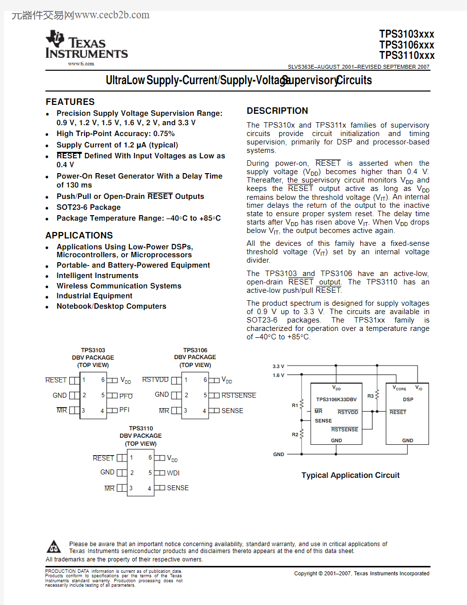
(TOP VIEW)
RESET
GND
MR
TPS3103
DBV PACKAGE
(TOP VIEW)
RSTVDD
GND
MR
TPS3106
DBV PACKAGE
(TOP VIEW)
V
DD
SENSE
TPS3110
DBV PACKAGE
WDI Typical Application Circuit
3.3 V
1.6 V
GND
TPS3103xxx
TPS3106xxx
TPS3110xxx
SLVS363E–AUGUST2001–REVISED SEPTEMBER2007 https://www.doczj.com/doc/9b10254544.html,
UltraLow Supply-Current/Supply-Voltage Supervisory Circuits
?Precision Supply Voltage Supervision Range:
0.9V,1.2V,1.5V,1.6V,2V,and3.3V The TPS310x and TPS311x families of supervisory
circuits provide circuit initialization and timing ?High Trip-Point Accuracy:0.75%
supervision,primarily for DSP and processor-based ?Supply Current of1.2μA(typical)
systems.
?RESET Defined With Input Voltages as Low as
During power-on,RESET is asserted when the
0.4V
supply voltage(V DD)becomes higher than0.4V.
?Power-On Reset Generator With a Delay Time Thereafter,the supervisory circuit monitors V
DD
and of130ms keeps the RESET output active as long as V
DD ?Push/Pull or Open-Drain RESET Outputs remains below the threshold voltage(V IT).An internal
timer delays the return of the output to the inactive ?SOT23-6Package
state to ensure proper system reset.The delay time ?Package Temperature Range:–40°C to+85°C starts after V
DD
has risen above V IT.When V DD drops
below V IT,the output becomes active again.
All the devices of this family have a fixed-sense ?Applications Using Low-Power DSPs,
threshold voltage(V IT)set by an internal voltage Microcontrollers,or Microprocessors
divider.
?Portable-and Battery-Powered Equipment
The TPS3103and TPS3106have an active-low,?Intelligent Instruments
open-drain RESET output.The TPS3110has an ?Wireless Communication Systems active-low push/pull RESET.
?Industrial Equipment
The product spectrum is designed for supply voltages ?Notebook/Desktop Computers
of0.9V up to3.3V.The circuits are available in
SOT23-6packages.The TPS31xx family is
characterized for operation over a temperature range
of–40°C to+85°C.
Please be aware that an important notice concerning availability,standard warranty,and use in critical applications of
Texas Instruments semiconductor products and disclaimers thereto appears at the end of this data sheet.
元器件交易网https://www.doczj.com/doc/9b10254544.html,
https://www.doczj.com/doc/9b10254544.html,
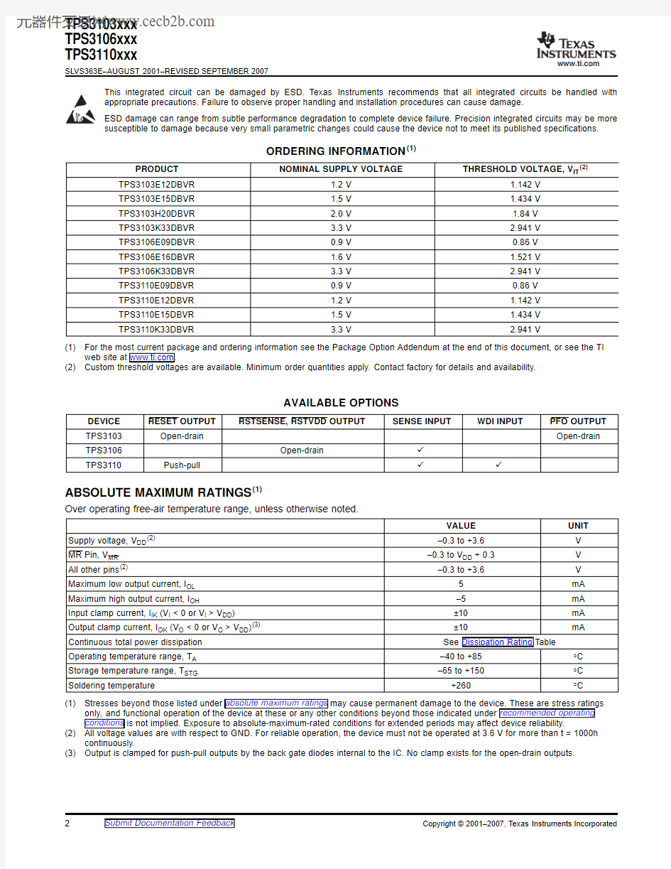
ABSOLUTE MAXIMUM RATINGS (1)
TPS3103xxx
TPS3106xxx TPS3110xxx
SLVS363E–AUGUST 2001–REVISED SEPTEMBER 2007
This integrated circuit can be damaged by ESD.Texas Instruments recommends that all integrated circuits be handled with appropriate precautions.Failure to observe proper handling and installation procedures can cause damage.
ESD damage can range from subtle performance degradation to complete device failure.Precision integrated circuits may be more susceptible to damage because very small parametric changes could cause the device not to meet its published specifications.
ORDERING INFORMATION (1)
PRODUCT NOMINAL SUPPLY VOLTAGE
THRESHOLD VOLTAGE,V IT (2)
TPS3103E12DBVR 1.2V 1.142V TPS3103E15DBVR 1.5V 1.434V TPS3103H20DBVR 2.0V 1.84V TPS3103K33DBVR 3.3V 2.941V TPS3106E09DBVR 0.9V 0.86V TPS3106E16DBVR 1.6V 1.521V TPS3106K33DBVR 3.3V 2.941V TPS3110E09DBVR 0.9V 0.86V TPS3110E12DBVR 1.2V 1.142V TPS3110E15DBVR 1.5V 1.434V TPS3110K33DBVR
3.3V
2.941V
(1)For the most
current package and ordering information see the Package Option Addendum at the end of this document,or see the TI web site at https://www.doczj.com/doc/9b10254544.html, .
(2)
Custom are available.Minimum order quantities apply.Contact factory for details and availability.
AVAILABLE OPTIONS
DEVICE RESET OUTPUT RSTSENSE,RSTVDD OUTPUT
SENSE INPUT
WDI INPUT
PFO OUTPUT TPS3103Open-drain
Open-drain
TPS3106Open-drain
üTPS3110
Push-pull ü
ü
Over operating free-air temperature range,unless otherwise noted.
(1)Stresses beyond those listed under absolute maximum ratings may cause permanent damage to the device.These are stress ratings only,and functional operation of the conditions beyond those indicated under recommended operating conditions is not implied.Exposure to absolute-maximum-rated conditions for extended periods may affect (2)values are with respect to GND.For reliable operation,the device must not be operated at 3.6V for more than t =1000h continuously.
(3)
Output is clamped for push-pull outputs by the back gate diodes internal to the IC.No clamp exists for the open-drain outputs.
元器件交易网https://www.doczj.com/doc/9b10254544.html,
https://www.doczj.com/doc/9b10254544.html,
DISSIPATION RATINGS
RECOMMENDED OPERATING CONDITIONS ELECTRICAL CHARACTERISTICS
TPS3103xxx
TPS3106xxx
TPS3110xxx SLVS363E–AUGUST2001–REVISED SEPTEMBER2007
T A≤+25°C DERATING FACTOR T A=+70°C T A=+85°C PACKAGE POWER RATING ABOVE T A=+25°C POWER RATING POWER RATING DBV437mW 3.5mW/°C280mW227mW
Over operating free-air temperature range,unless otherwise noted.
MIN MAX UNIT Supply voltage,V DD(1)0.4 3.3V
Input voltage,V I0V DD+0.3V
High-level input voltage,V IH at MR,WDI0.7×V DD V
Low-level input voltage,V IL at MR,WDI0.3×V DD V
Input transition rise and fall rate atΔt/ΔV at MR,WDI100ns/V
Operating temperature range,T A–40+85°C
(1)For proper operation of SENSE,PFI,and WDI functions:V DD≥0.8V.
Over operating free-air temperature range(unless otherwise noted).
PARAMETER TEST CONDITIONS MIN TYP MAX UNIT
V DD=3.3V,I OH=–3mA
V DD=1.8V,I OH=–2mA
0.8×V DD V
V OH High-level output voltage V DD=1.5V,I OH=–1mA
V DD=0.9V,I OH=–0.4mA
V DD=0.5V,I OH=–5μA0.7×V DD V
V DD=3.3V,I OL=3mA
V DD=1.5V,I OL=2mA
V OL Low-level output voltage0.3V
V DD=1.2V,I OL=1mA
V DD=0.9V,I OL=500μA
V OL Low-level output voltage RESET only V DD=0.4V,I OL=5μA0.1V
TPS31xxE090.8540.8600.866
TPS31xxE12 1.133 1.142 1.151
TPS31xxE15 1.423 1.434 1.445 Negative-going input
V IT–T A=+25°C V threshold voltage(1)TPS31xxE16 1.512 1.523 1.534
TPS31xxH20 1.829 1.843 1.857
TPS31xxK33 2.919 2.941 2.963
Negative-going input
V IT–(S)SENSE,PFI V DD≥0.8V,T A=+25°C0.5420.5510.559V threshold voltage(1)
0.8V≤V IT<1.5V20
V HYS Hysteresis at V DD input 1.6V≤V IT<2.4V30mV
2.5V≤V IT<
3.3V50
Temperature coefficient of V IT?,PFI,
T(K)T A=–40°C to+85°C–0.012–0.019%/K SENSE
V HYS Hysteresis at SENSE,PFI input V DD≥0.8V15mV
MR MR=V DD,V DD=3.3V–2525
I IH High-level input current nA
SENSE,PFI,SENSE,PFI,WDI=V DD,
–2525
WDI V DD=3.3V
(1)To ensure the best stability of the threshold voltage,a bypass capacitor(ceramic,0.1μF)should be placed close to the supply
元器件交易网https://www.doczj.com/doc/9b10254544.html,
https://www.doczj.com/doc/9b10254544.html,
SWITCHING CHARACTERISTICS
TIMING REQUIREMENTS
TPS3103xxx
TPS3106xxx TPS3110xxx
SLVS363E–AUGUST 2001–REVISED SEPTEMBER 2007
ELECTRICAL CHARACTERISTICS (continued)
Over operating free-air temperature range (unless otherwise noted).
PARAMETER
TEST CONDITIONS MIN TYP MAX UNIT MR
MR =0V,V DD =3.3V –47–33
–25μA I IL Low-level input current SENSE,PFI,SENSE,PFI,WDI =0V,–25
25nA WDI V DD =3.3V
High-level output current I OH
Open-drain
V DD =V IT +0.2V,V OH =3.3V 200nA
at RESET (2)
V DD >V IT (average current), 1.23V DD <1.8V
V DD >V IT (average current),2
4.5I DD
Supply current
μA V DD >1.8V
V DD
27Internal pull-up resistor at MR
70
100130
k ?C I Input capacitance at MR,SENSE,PFI,WDI V I =0V to V DD
1pF (2)
Also refers to RSTVDD and RSTSENSE.
At R L =1M ?,C L =50pF,and T A =–40°C to +85°C,unless otherwise noted.
PARAMETER
TEST CONDITIONS
MIN TYP MAX UNIT t D Delay time
V DD ≥1.1×V IT ,MR =0.7×V DD ,See Timing Diagrams 65
130
195ms Propagation delay time,V DD to RESET or t PHL V IH =1.1×V IT ,V IL =0.9×V IT 40μs high-to-low level output RSTVDD delay Propagation delay time,V DD to RESET or t PLH V IH =1.1×V IT ,V IL =0.9×V IT
40μs low-to-high level output RSTVDD delay Propagation delay time,SENSE to RESET or t PHL V DD ≥0.8V,V IH =1.1×V IT ,V IL =0.9×V IT 40μs high-to-low level output RSTSENSE delay Propagation delay time,SENSE to RESET or t PLH V DD ≥0.8V,V IH =1.1×V IT ,V IL =0.9×V IT 40μs high-to-low level output RSTSENSE delay Propagation delay time,t PHL PFI to PFO delay V DD ≥0.8V,V IH =1.1×V IT ,V IL =0.9×V IT 40μs high-to-low level output Propagation delay time,t PLH PFI to PFO delay V DD ≥0.8V,V IH =1.1×V IT ,V IL =0.9×V IT 300μs low-to-high level output MR to RESET.Propagation delay time,t PHL
RSTVDD,
V DD ≥1.1×V IT ,V IL =0.3×V DD ,V IH =0.7×V DD
1
5
μs
low-to-high level output RSTSENSE delay MR to RESET.Propagation delay time,t PLH RSTVDD,
V DD ≥1.1×V IT ,V IL =0.3×V DD ,V IH =0.7×V DD 15μs
low-to-high level output
RSTSENSE delay
At R L =1M ?,C L =50pF,and T A =–40°C to +85°C,unless otherwise noted.
PARAMETER
TEST CONDITIONS
MIN TYP MAX UNIT t T(OUT)
Time-out period
at WDI V DD ≥0.85V
0.55 1.1
1.65
s
at V DD V IH =1.1×V IT ,V IL =0.9×V IT–,V IT–=0.86V 20at MR
V DD ≥V IT +0.2V,V IL =0.3×V DD ,V IH =0.7×V DD 0.1t W
Pulse width
at SENSE V DD ≥V IT ,V IH =1.1×V IT ?(S),V IL =0.9×V IT ?(S)20μs
at PFI V DD ≥0.85V,V IH =1.1×V IT ?(S),V IL =0.9×V IT ?(S)20at WDI
V DD ≥V IT ,V IL =0.3×V DD ,V IH =0.7×V DD
0.3
元器件交易网https://www.doczj.com/doc/9b10254544.html,
https://www.doczj.com/doc/9b10254544.html,
FUNCTIONAL BLOCK DIAGRAMS
V DD MR
PFI GND
RESET
PFO TPS3103
V DD MR
SENSE
GND
RSTSENSE
TPS3106
TPS3103xxx
TPS3106xxx
TPS3110xxx
SLVS363E–AUGUST2001–REVISED SEPTEMBER2007
元器件交易网https://www.doczj.com/doc/9b10254544.html,
https://www.doczj.com/doc/9b10254544.html,
V DD
MR SENSE
GND RESET
WDI TPS3110
TPS3103xxx
TPS3106xxx
TPS3110xxx
SLVS363E–AUGUST2001–REVISED SEPTEMBER2007
Table1.TPS3103FUNCTION TABLE
MR V(PFI)>0.551V V DD>V IT RESET PFO
L0X(1)L L
L1X L H
H00L L
H01H L
H10L H
H11H H
(1)X=Don’t care.
Table2.TPS3106FUNCTION TABLE
MR V(SENSE)>0.551V V DD>V IT RSTVDD RSTSENSE
L X(1)X L L
H00L L
H01H L
H10L H
H11H H
(1)X=Don’t care.
Table3.TPS3110FUNCTION TABLE(1)
MR V(SENSE)>0.551V V DD>V IT RESET
L X(2)X L
H00L
H01L
H10L
H11H
(1)Function of watchdog-timer not shown.
(2)X=Don’t care.
元器件交易网https://www.doczj.com/doc/9b10254544.html,
https://www.doczj.com/doc/9b10254544.html,
PIN DESCRIPTIONS
(TOP VIEW)
RSTVDD
GND MR
V DD
SENSE
TPS3106DBV PACKAGE RSTSENSE 3
24
615(TOP VIEW)
V DD PFI
TPS3103DBV PACKAGE PFO (TOP VIEW)
RESET GND MR
V DD SENSE
TPS3110DBV PACKAGE WDI 3
24
615TPS3103xxx TPS3106xxx TPS3110xxx
SLVS363E–AUGUST 2001–REVISED SEPTEMBER 2007
TERMINAL FUNCTIONS
TERMINAL
DESCRIPTION NAME DEVICE NO.GND ALL 2GND
Manual-reset input.Pull low to force a reset.RESET remains low as long as MR is low and for MR ALL 3the timeout period after MR goes high.Leave unconnected or connect to V DD when unused.PFI TPS31034Power-fail input compares to 0.551V with no additional delay.Connect to V DD if not used.PFO TPS31035Power-fail output.Goes high when voltage at PFI rises above 0.551V.TPS3103,RESET 1Active-low reset output.Either push-pull or open-drain output stage.
TPS3110Active-low reset output.Logic level at RSTSENSE only depends on the voltage at SENSE and RSTSENSE TPS31065the status of MR.
Active-low reset output.Logic level at RSTVDD only depends on the voltage at V DD and the RSTVDD TPS31061status of MR.
TPS3106,A reset will be asserted if the voltage at SENSE is lower than 0.551V.Connect to V DD if SENSE 4TPS3110unused.
V DD ALL 6Supply voltage.Powers the device and monitors its own voltage.
Watchdog timer input.If WDI remains high or low longer than the time-out period,then reset is WDI
TPS3110
5
triggered.The timer clears when reset is asserted or when WDI sees a rising edge or a falling edge.
元器件交易网https://www.doczj.com/doc/9b10254544.html,
https://www.doczj.com/doc/9b10254544.html,
TIMING DIAGRAMS
Timing Diagrams for TPS3103
V
IT (S)-V IT (S)-TPS3103xxx
TPS3106xxx TPS3110xxx
SLVS363E–AUGUST 2001–REVISED SEPTEMBER 2007
元器件交易网https://www.doczj.com/doc/9b10254544.html,
https://www.doczj.com/doc/9b10254544.html,
Timing Diagram for TPS3106
t
V IT -TPS3103xxx TPS3106xxx TPS3110xxx
SLVS363E–AUGUST 2001–REVISED SEPTEMBER 2007
元器件交易网https://www.doczj.com/doc/9b10254544.html,
https://www.doczj.com/doc/9b10254544.html,
Timing Diagram for TPS3110
t
V IT (S)-
TYPICAL CHARACTERISTICS
02468101214161820I S u p p l y C u r r e n t --
m A
D D V Supply Voltage -V
-DD 0
0.05
0.10
0.15
0.20
0.25
0.30
0.20.40.60.8 1.0 1.2 1.4 1.6 1.8 2.0
V L o w -L e v e l O u t p u t V o l t a g e V
O L --I Low-Level Output Current OL --mA
TPS3103xxx
TPS3106xxx TPS3110xxx
SLVS363E–AUGUST 2001–REVISED SEPTEMBER 2007
TPS3110E09TPS3110E09
SUPPLY CURRENT
LOW-LEVEL OUTPUT VOLTAGE
vs
vs
SUPPLY VOLTAGE
LOW-LEVEL OUTPUT CURRENT
Figure 1.
Figure 2.
元器件交易网https://www.doczj.com/doc/9b10254544.html,
https://www.doczj.com/doc/9b10254544.html,
1.0V L o w -L e v e l O u t p u t V o l t a g e V
O L --I Low-Level Output Current OL --
mA
0.60
0.65
0.70
0.75
0.80
0.85
0.90
-0.5
-0.4-0.3
-0.2
-0.1
I High-Level Output Current --OH mA
V H i g h -L e v e l O u t p u t V o l t a g e V
O H --2.0
3.0
-25
-20
-15
-10
-5
V H i g h -L e v e l o u t p u t V o l t a g e V
O H --I Low-Level Output Current OH --mA
0.1
0.20.30.40.5
V Threshold Overdrive Voltage --V
DD t V M i n i m u m P u l s e D u r a t i o n a t --m s
W D D TPS3103xxx TPS3106xxx TPS3110xxx
SLVS363E–AUGUST 2001–REVISED SEPTEMBER 2007
TYPICAL CHARACTERISTICS (continued)
TPS3110E09
TPS3110E09
LOW-LEVEL OUTPUT VOLTAGE
HIGH-LEVEL OUTPUT VOLTAGE
vs
vs
LOW-LEVEL OUTPUT CURRENT
HIGH-LEVEL OUTPUT CURRENT
Figure 3.Figure 4.TPS3110K33
HIGH-LEVEL OUTPUT VOLTAGE
MINIMUM PULSE DURATION AT V DD
vs
vs
HIGH-LEVEL OUTPUT CURRENT
THRESHOLD OVERDRIVE VOLTAGE
Figure 5.
Figure 6.
元器件交易网https://www.doczj.com/doc/9b10254544.html,
https://www.doczj.com/doc/9b10254544.html,
0.992
0.9940.9960.9981.0001.0021.0041.0061.008-50
50100
V N o r m a l i z e d T h r e s h o l d V o l t a g e I T --V
T Free-Air T emperature A --°C
TPS3103xxx
TPS3106xxx TPS3110xxx
SLVS363E–AUGUST 2001–REVISED SEPTEMBER 2007
TYPICAL CHARACTERISTICS (continued)
NORMALIZED THRESHOLD VOLTAGE
vs
FREE-AIR TEMPERATURE
Figure 7.
元器件交易网https://www.doczj.com/doc/9b10254544.html,
https://www.doczj.com/doc/9b10254544.html,
APPLICATION INFORMATION
R1+R2 ǒ
V TRIP
V IT (S )
*1ǔ
(1)
2 Cell NiMH
Reset Output
TPS3103xxx TPS3106xxx TPS3110xxx
SLVS363E–AUGUST 2001–REVISED SEPTEMBER 2007
The TPS31xx family has a quiescent current in the 1-μA to 2-μA range.When RESET is active,triggered by the voltage monitored at V DD ,the quiescent current increases to about 20μA (see the Electrical Characteristics ).In some applications it is necessary to minimize the quiescent current even during the reset period.This is especially true when the voltage of a battery is supervised and the RESET is used to shut down the system or for an early warning.In this case the reset condition will last for a longer period of time.The current drawn from the battery should almost be zero,especially when the battery is discharged.
For this kind of application,either the TPS3103or TPS3106is a good fit.To minimize current consumption,select a version where the threshold voltage is lower than the voltage monitored at V DD .The TPS3106has two reset outputs.One output (RSTVDD)is triggered from the voltage monitored at V DD .The other output (RSTSENSE)is triggered from the voltage monitored at SENSE.In the application shown in Figure 8,the TPS3106E09is used to monitor the input voltage of two NiCd or NiMH cells.The threshold (TH)0.86V)was chosen as low as possible to ensure that the supply voltage is always higher than the threshold voltage at V DD .The voltage of the battery is monitored using the SENSE input.The voltage divider was calculated to assert a reset using the RSTSENSE output at 2×0.8V =1.6V.
where:
V TRIP is the voltage of the battery at which a reset is asserted and V IT(S)is the threshold voltage at SENSE =0.551V.R1was chosen for a resistor current in the 1-μA range.With V TRIP =1.6V:R1≡1.9×R2
R1=820k ?,R2=430k ?
Figure 8.Battery Monitoring with 3-μA Supply Current for Device and Resistor Divider
元器件交易网https://www.doczj.com/doc/9b10254544.html,
https://www.doczj.com/doc/9b10254544.html,
WATCHDOG
MANUAL RESET (MR)
PFI,PFO
SENSE
TPS3103xxx
TPS3106xxx TPS3110xxx
SLVS363E–AUGUST 2001–REVISED SEPTEMBER 2007
The TPS3110device integrates a watchdog timer that must be periodically triggered by a positive or negative transition of WDI.When the supervising system fails to retrigger the watchdog circuit within the time-out interval,RESET becomes active for the time period (t D ).This event also reinitializes the watchdog timer.
Many μC-based products require manual-reset capability,allowing an operator or logic circuitry to initiate a reset.Logic low at MR asserts reset.Reset remains asserted while MR is low and for a time period (t D )after MR returns high.The input has an internal 100-k ?pull-up resistor,so it can be left open if it is unused.
Connect a normally open momentary switch from MR to GND to create a manual reset function.External debounce is not required.If MR is driven from long cables or if the device is used in noisy environments,connecting a 0.1-μF capacitor from MR to GND provides additional noise immunity.
If there is a possibility of transient or DC conditions causing MR to rise above V DD ,a diode should be used to limit MR to a diode drop above V DD .
The TPS3103has an integrated power-fail (PFI)comparator with a separate open-drain (PFO)output.The PFI and PFO can be used for low-battery detection,power-fail warning,or for monitoring a power supply other than the main supply,and has no effect on RESET.
An additional comparator is provided to monitor voltages other than the nominal supply voltage.The power-fail input (PFI)will be compared with an internal voltage reference of 0.551V.If the input voltage falls below the power-fail threshold (V IT –(S)),the power-fail output (PFO)goes low.If it goes above 0.551V plus approximately 15-mV hysteresis,the output returns to high.By connecting two external resistors,it is possible to supervise any voltage above 0.551V.The sum of both resistors should be approximately 1M ?,to minimize power consumption and to assure that the current into the PFI pin can be neglected,compared with the current through the resistor network.The tolerance of the external resistors should be not more than 1%to ensure minimal variation of sensed voltage.If the power-fail comparator is unused,connect PFI to GND and leave PFO unconnected.For proper operation of the PFI-comparator,the supply voltage (V DD )must be higher than 0.8V.
The voltage at the SENSE input is compared with a reference voltage of 0.551V.If the voltage at SENSE falls below the sense-threshold (V IT ?(S)),reset is asserted.On the TPS3106,a dedicated RSTSENSE output is available.On the TPS3110,the logic signal from SENSE is OR-wired with the logic signal from V DD or MR.An internal timer delays the return of the output to the inactive state,once the voltage at SENSE goes above 0.551V plus about 15mV of hysteresis.For proper operation of the SENSE-comparator,the supply voltage must be higher than 0.8V.
元器件交易网https://www.doczj.com/doc/9b10254544.html,
https://www.doczj.com/doc/9b10254544.html,
(1) Resistor may be integrated in m C.
2 V
-2 V
V = 0.551 V (NEG_TH)
-R2R1(V 0.551 V)
DD -GND
V (CORE_TH)3.3 V 1.5 V
TPS3103xxx TPS3106xxx TPS3110xxx
SLVS363E–AUGUST 2001–REVISED SEPTEMBER 2007
Figure 9.TPS3103Monitoring a Negative Voltage
Figure 10.TPS3110in a DSP-System Monitoring Both Supply Voltages
元器件交易网https://www.doczj.com/doc/9b10254544.html,
PACKAGING INFORMATION
Orderable Device Status(1)Package
Type Package
Drawing
Pins Package
Qty
Eco Plan(2)Lead/Ball Finish MSL Peak Temp(3)
SN0402002DBVR ACTIVE SOT-23DBV6TBD Call TI Call TI
TPS3103E12DBVR ACTIVE SOT-23DBV63000Green(RoHS&
no Sb/Br)
CU NIPDAU Level-1-260C-UNLIM
TPS3103E12DBVRG4ACTIVE SOT-23DBV63000Green(RoHS&
no Sb/Br)
CU NIPDAU Level-1-260C-UNLIM
TPS3103E12DBVT ACTIVE SOT-23DBV6250Green(RoHS&
no Sb/Br)
CU NIPDAU Level-1-260C-UNLIM
TPS3103E12DBVTG4ACTIVE SOT-23DBV6250Green(RoHS&
no Sb/Br)
CU NIPDAU Level-1-260C-UNLIM
TPS3103E15DBVR ACTIVE SOT-23DBV63000Green(RoHS&
no Sb/Br)
CU NIPDAU Level-1-260C-UNLIM
TPS3103E15DBVRG4ACTIVE SOT-23DBV63000Green(RoHS&
no Sb/Br)
CU NIPDAU Level-1-260C-UNLIM
TPS3103E15DBVT ACTIVE SOT-23DBV6250Green(RoHS&
no Sb/Br)
CU NIPDAU Level-1-260C-UNLIM
TPS3103E15DBVTG4ACTIVE SOT-23DBV6250Green(RoHS&
no Sb/Br)
CU NIPDAU Level-1-260C-UNLIM
TPS3103H20DBVR ACTIVE SOT-23DBV63000Green(RoHS&
no Sb/Br)
CU NIPDAU Level-1-260C-UNLIM
TPS3103H20DBVRG4ACTIVE SOT-23DBV63000Green(RoHS&
no Sb/Br)
CU NIPDAU Level-1-260C-UNLIM
TPS3103H20DBVT ACTIVE SOT-23DBV6250Green(RoHS&
no Sb/Br)
CU NIPDAU Level-1-260C-UNLIM
TPS3103H20DBVTG4ACTIVE SOT-23DBV6250Green(RoHS&
no Sb/Br)
CU NIPDAU Level-1-260C-UNLIM
TPS3103K33DBVR ACTIVE SOT-23DBV63000Green(RoHS&
no Sb/Br)
CU NIPDAU Level-1-260C-UNLIM
TPS3103K33DBVRG4ACTIVE SOT-23DBV63000Green(RoHS&
no Sb/Br)
CU NIPDAU Level-1-260C-UNLIM
TPS3103K33DBVT ACTIVE SOT-23DBV6250Green(RoHS&
no Sb/Br)
CU NIPDAU Level-1-260C-UNLIM
TPS3103K33DBVTG4ACTIVE SOT-23DBV6250Green(RoHS&
no Sb/Br)
CU NIPDAU Level-1-260C-UNLIM
TPS3106E09DBVR ACTIVE SOT-23DBV63000Green(RoHS&
no Sb/Br)
CU NIPDAU Level-1-260C-UNLIM
TPS3106E09DBVRG4ACTIVE SOT-23DBV63000Green(RoHS&
no Sb/Br)
CU NIPDAU Level-1-260C-UNLIM
TPS3106E09DBVT ACTIVE SOT-23DBV6250Green(RoHS&
no Sb/Br)
CU NIPDAU Level-1-260C-UNLIM
TPS3106E09DBVTG4ACTIVE SOT-23DBV6250Green(RoHS&
no Sb/Br)
CU NIPDAU Level-1-260C-UNLIM
TPS3106E16DBVR ACTIVE SOT-23DBV63000Green(RoHS&
no Sb/Br)
CU NIPDAU Level-1-260C-UNLIM
TPS3106E16DBVRG4ACTIVE SOT-23DBV63000Green(RoHS&
no Sb/Br)
CU NIPDAU Level-1-260C-UNLIM
TPS3106E16DBVT ACTIVE SOT-23DBV6250Green(RoHS&
no Sb/Br)
CU NIPDAU Level-1-260C-UNLIM
TPS3106E16DBVTG4ACTIVE SOT-23DBV6250Green(RoHS&
no Sb/Br)
CU NIPDAU Level-1-260C-UNLIM
Orderable Device Status(1)Package
Type Package
Drawing
Pins Package
Qty
Eco Plan(2)Lead/Ball Finish MSL Peak Temp(3)
TPS3106K33DBVR ACTIVE SOT-23DBV63000Green(RoHS&
no Sb/Br)
CU NIPDAU Level-1-260C-UNLIM
TPS3106K33DBVRG4ACTIVE SOT-23DBV63000Green(RoHS&
no Sb/Br)
CU NIPDAU Level-1-260C-UNLIM
TPS3106K33DBVT ACTIVE SOT-23DBV6250Green(RoHS&
no Sb/Br)
CU NIPDAU Level-1-260C-UNLIM
TPS3106K33DBVTG4ACTIVE SOT-23DBV6250Green(RoHS&
no Sb/Br)
CU NIPDAU Level-1-260C-UNLIM
TPS3110E09DBVR ACTIVE SOT-23DBV63000Green(RoHS&
no Sb/Br)
CU NIPDAU Level-1-260C-UNLIM
TPS3110E09DBVRG4ACTIVE SOT-23DBV63000Green(RoHS&
no Sb/Br)
CU NIPDAU Level-1-260C-UNLIM
TPS3110E09DBVT ACTIVE SOT-23DBV6250Green(RoHS&
no Sb/Br)
CU NIPDAU Level-1-260C-UNLIM
TPS3110E09DBVTG4ACTIVE SOT-23DBV6250Green(RoHS&
no Sb/Br)
CU NIPDAU Level-1-260C-UNLIM
TPS3110E12DBVR ACTIVE SOT-23DBV63000Green(RoHS&
no Sb/Br)
CU NIPDAU Level-1-260C-UNLIM
TPS3110E12DBVRG4ACTIVE SOT-23DBV63000Green(RoHS&
no Sb/Br)
CU NIPDAU Level-1-260C-UNLIM
TPS3110E12DBVT ACTIVE SOT-23DBV6250Green(RoHS&
no Sb/Br)
CU NIPDAU Level-1-260C-UNLIM
TPS3110E12DBVTG4ACTIVE SOT-23DBV6250Green(RoHS&
no Sb/Br)
CU NIPDAU Level-1-260C-UNLIM
TPS3110E15DBVR ACTIVE SOT-23DBV63000Green(RoHS&
no Sb/Br)
CU NIPDAU Level-1-260C-UNLIM
TPS3110E15DBVRG4ACTIVE SOT-23DBV63000Green(RoHS&
no Sb/Br)
CU NIPDAU Level-1-260C-UNLIM
TPS3110E15DBVT ACTIVE SOT-23DBV6250Green(RoHS&
no Sb/Br)
CU NIPDAU Level-1-260C-UNLIM
TPS3110E15DBVTG4ACTIVE SOT-23DBV6250Green(RoHS&
no Sb/Br)
CU NIPDAU Level-1-260C-UNLIM
TPS3110K33DBVR ACTIVE SOT-23DBV63000Green(RoHS&
no Sb/Br)
CU NIPDAU Level-1-260C-UNLIM
TPS3110K33DBVRG4ACTIVE SOT-23DBV63000Green(RoHS&
no Sb/Br)
CU NIPDAU Level-1-260C-UNLIM
TPS3110K33DBVT ACTIVE SOT-23DBV6250Green(RoHS&
no Sb/Br)
CU NIPDAU Level-1-260C-UNLIM
TPS3110K33DBVTG4ACTIVE SOT-23DBV6250Green(RoHS&
no Sb/Br)
CU NIPDAU Level-1-260C-UNLIM
(1)The marketing status values are defined as follows:
ACTIVE:Product device recommended for new designs.
LIFEBUY:TI has announced that the device will be discontinued,and a lifetime-buy period is in effect.
NRND:Not recommended for new designs.Device is in production to support existing customers,but TI does not recommend using this part in a new design.
PREVIEW:Device has been announced but is not in production.Samples may or may not be available.
OBSOLETE:TI has discontinued the production of the device.
(2)Eco Plan-The planned eco-friendly classification:Pb-Free(RoHS),Pb-Free(RoHS Exempt),or Green(RoHS&no Sb/Br)-please check https://www.doczj.com/doc/9b10254544.html,/productcontent for the latest availability information and additional product content details.
TBD:The Pb-Free/Green conversion plan has not been defined.
Pb-Free(RoHS):TI's terms"Lead-Free"or"Pb-Free"mean semiconductor products that are compatible with the current RoHS requirements for all6substances,including the requirement that lead not exceed0.1%by weight in homogeneous materials.Where designed to be soldered
at high temperatures,TI Pb-Free products are suitable for use in specified lead-free processes.
Pb-Free(RoHS Exempt):This component has a RoHS exemption for either1)lead-based flip-chip solder bumps used between the die and package,or2)lead-based die adhesive used between the die and leadframe.The component is otherwise considered Pb-Free(RoHS compatible)as defined above.
Green(RoHS&no Sb/Br):TI defines"Green"to mean Pb-Free(RoHS compatible),and free of Bromine(Br)and Antimony(Sb)based flame retardants(Br or Sb do not exceed0.1%by weight in homogeneous material)
(3)MSL,Peak Temp.--The Moisture Sensitivity Level rating according to the JEDEC industry standard classifications,and peak solder temperature.
Important Information and Disclaimer:The information provided on this page represents TI's knowledge and belief as of the date that it is provided.TI bases its knowledge and belief on information provided by third parties,and makes no representation or warranty as to the accuracy of such information.Efforts are underway to better integrate information from third parties.TI has taken and continues to take reasonable steps to provide representative and accurate information but may not have conducted destructive testing or chemical analysis on incoming materials and chemicals.TI and TI suppliers consider certain information to be proprietary,and thus CAS numbers and other limited information may not be available for release.
In no event shall TI's liability arising out of such information exceed the total purchase price of the TI part(s)at issue in this document sold by TI to Customer on an annual basis.
TAPE AND REEL INFORMATION
*All dimensions are nominal
Device
Package Type Package Drawing Pins SPQ
Reel Diameter (mm)Reel Width W1(mm)A0(mm)B0(mm)K0(mm)
P1(mm)W (mm)Pin1Quadrant TPS3103E12DBVR SOT-23DBV 63000179.08.4 3.2 3.2 1.4 4.08.0Q3TPS3103E12DBVT SOT-23DBV 6250179.08.4 3.2 3.2 1.4 4.08.0Q3TPS3103E15DBVR SOT-23DBV 63000179.08.4 3.2 3.2 1.4 4.08.0Q3TPS3103E15DBVT SOT-23DBV 6250179.08.4 3.2 3.2 1.4 4.08.0Q3TPS3103H20DBVR SOT-23DBV 63000179.08.4 3.2 3.2 1.4 4.08.0Q3TPS3103H20DBVT SOT-23DBV 6250179.08.4 3.2 3.2 1.4 4.08.0Q3TPS3103K33DBVR SOT-23DBV 63000180.09.0 3.15 3.2 1.4 4.08.0Q3TPS3103K33DBVR SOT-23DBV 63000179.08.4 3.2 3.2 1.4 4.08.0Q3TPS3103K33DBVT SOT-23DBV 6250180.09.0 3.15 3.2 1.4 4.08.0Q3TPS3103K33DBVT SOT-23DBV 6250179.08.4 3.2 3.2 1.4 4.08.0Q3TPS3106E09DBVR SOT-23DBV 63000180.09.0 3.15 3.2 1.4 4.08.0Q3TPS3106E09DBVT SOT-23DBV 6250180.09.0 3.15 3.2 1.4 4.08.0Q3TPS3106E16DBVR SOT-23DBV 63000180.09.0 3.15 3.2 1.4 4.08.0Q3TPS3106E16DBVT SOT-23DBV 6250180.09.0 3.15 3.2 1.4 4.08.0Q3TPS3106K33DBVR SOT-23DBV 63000180.09.0 3.15 3.2 1.4 4.08.0Q3TPS3106K33DBVT SOT-23DBV 6250180.09.0 3.15 3.2 1.4 4.08.0Q3TPS3110E09DBVR SOT-23DBV 63000180.09.0 3.15 3.2 1.4 4.08.0Q3TPS3110E09DBVT
SOT-23
DBV
6
250
180.0
9.0
3.15
3.2
1.4
4.0
8.0
Q3
Device Package
Type Package
Drawing
Pins SPQ Reel
Diameter
(mm)
Reel
Width
W1(mm)
A0(mm)B0(mm)K0(mm)P1
(mm)
W
(mm)
Pin1
Quadrant
TPS3110E12DBVR SOT-23DBV63000180.09.0 3.15 3.2 1.4 4.08.0Q3 TPS3110E12DBVT SOT-23DBV6250180.09.0 3.15 3.2 1.4 4.08.0Q3 TPS3110E15DBVR SOT-23DBV63000180.09.0 3.15 3.2 1.4 4.08.0Q3 TPS3110E15DBVT SOT-23DBV6250180.09.0 3.15 3.2 1.4 4.08.0Q3 TPS3110K33DBVR SOT-23DBV63000180.09.0 3.15 3.2 1.4 4.08.0Q3 TPS3110K33DBVT SOT-23DBV6250180.09.0 3.15 3.2 1.4 4.08.0Q3
*All dimensions are nominal
Device Package Type Package Drawing Pins SPQ Length(mm)Width(mm)Height(mm) TPS3103E12DBVR SOT-23DBV63000195.0200.045.0
TPS3103E12DBVT SOT-23DBV6250195.0200.045.0
TPS3103E15DBVR SOT-23DBV63000195.0200.045.0
TPS3103E15DBVT SOT-23DBV6250195.0200.045.0
TPS3103H20DBVR SOT-23DBV63000195.0200.045.0
TPS3103H20DBVT SOT-23DBV6250195.0200.045.0
TPS3103K33DBVR SOT-23DBV63000182.0182.020.0
TPS3103K33DBVR SOT-23DBV63000195.0200.045.0
TPS3103K33DBVT SOT-23DBV6250182.0182.020.0
TPS3103K33DBVT SOT-23DBV6250195.0200.045.0
TPS3106E09DBVR SOT-23DBV63000182.0182.020.0