
April 2011Doc ID 13587 Rev 131/99
STM32F103x8STM32F103xB
Medium-density performance line ARM-based 32-bit MCU with 64 or 128 KB Flash, USB, CAN, 7 timers, 2 ADCs, 9 communication interfaces
Features
■
ARM 32-bit Cortex?-M3 CPU Core –72 MHz maximum frequency,
1.25 DMIPS/MHz (Dhrystone
2.1) performance at 0 wait state memory access
–Single-cycle multiplication and hardware division ■
Memories
–64 or 128 Kbytes of Flash memory –20 Kbytes of SRAM
■
Clock, reset and supply management
– 2.0 to 3.6V application supply and I/Os –POR, PDR, and programmable voltage detector (PVD)
–4-to-16 MHz crystal oscillator
–Internal 8 MHz factory-trimmed RC –Internal 40 kHz RC –PLL for CPU clock
–32 kHz oscillator for RTC with calibration ■
Low power
–Sleep, Stop and Standby modes
–V BAT supply for RTC and backup registers ■
2 x 12-bit, 1 μs A/D converters (up to 16 channels)
–Conversion range: 0 to 3.6 V –Dual-sample and hold capability –Temperature sensor
■
DMA
–7-channel DMA controller
–Peripherals supported: timers, ADC, SPIs, I 2Cs and USARTs ■
Up to 80 fast I/O ports
–26/37/51/80 I/Os, all mappable on 16 external interrupt vectors and almost all 5V-tolerant
■Debug mode
–Serial wire debug (SWD) & JTAG interfaces ■
7 timers
–Three 16-bit timers, each with up to 4 IC/OC/PWM or pulse counter and
quadrature (incremental) encoder input –16-bit, motor control PWM timer with dead-time generation and emergency stop – 2 watchdog timers (Independent and Window)
–SysTick timer 24-bit downcounter
■
Up to 9 communication interfaces
–Up to 2 x I 2C interfaces (SMBus/PMBus)–Up to 3 USARTs (ISO 7816 interface, LIN, IrDA capability, modem control)–Up to 2 SPIs (18 Mbit/s)–CAN interface (2.0B Active)–USB 2.0 full-speed interface ■CRC calculation unit, 96-bit unique ID ■
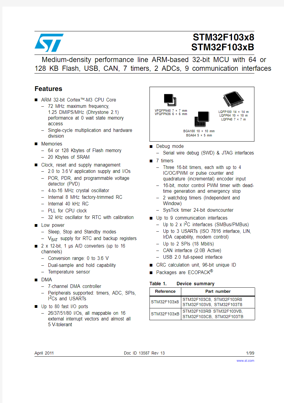
Packages are ECOPACK ?
Table 1.
Device summary
Reference
Part number
STM32F103x8STM32F103C8, STM32F103R8 STM32F103V8, STM32F103T8STM32F103xB
STM32F103RB STM32F103VB, STM32F103CB, STM32F103TB
https://www.doczj.com/doc/989666176.html,
Contents STM32F103x8, STM32F103xB
Contents
1Introduction . . . . . . . . . . . . . . . . . . . . . . . . . . . . . . . . . . . . . . . . . . . . . . . . 9
2Description . . . . . . . . . . . . . . . . . . . . . . . . . . . . . . . . . . . . . . . . . . . . . . . . . 9
2.1Device overview . . . . . . . . . . . . . . . . . . . . . . . . . . . . . . . . . . . . . . . . . . . . 10
2.2Full compatibility throughout the family . . . . . . . . . . . . . . . . . . . . . . . . . . 13
2.3Overview . . . . . . . . . . . . . . . . . . . . . . . . . . . . . . . . . . . . . . . . . . . . . . . . . 14
2.3.1ARM? Cortex?-M3 core with embedded Flash and SRAM . . . . . . . . . 14
2.3.2Embedded Flash memory . . . . . . . . . . . . . . . . . . . . . . . . . . . . . . . . . . . 14
2.3.3CRC (cyclic redundancy check) calculation unit . . . . . . . . . . . . . . . . . . 14
2.3.4Embedded SRAM . . . . . . . . . . . . . . . . . . . . . . . . . . . . . . . . . . . . . . . . . 14
2.3.5Nested vectored interrupt controller (NVIC) . . . . . . . . . . . . . . . . . . . . . . 14
2.3.6External interrupt/event controller (EXTI) . . . . . . . . . . . . . . . . . . . . . . . 15
2.3.7Clocks and startup . . . . . . . . . . . . . . . . . . . . . . . . . . . . . . . . . . . . . . . . . 15
2.3.8Boot modes . . . . . . . . . . . . . . . . . . . . . . . . . . . . . . . . . . . . . . . . . . . . . . 15
2.3.9Power supply schemes . . . . . . . . . . . . . . . . . . . . . . . . . . . . . . . . . . . . . 15
2.3.10Power supply supervisor . . . . . . . . . . . . . . . . . . . . . . . . . . . . . . . . . . . . 15
2.3.11Voltage regulator . . . . . . . . . . . . . . . . . . . . . . . . . . . . . . . . . . . . . . . . . . 16
2.3.12Low-power modes . . . . . . . . . . . . . . . . . . . . . . . . . . . . . . . . . . . . . . . . . 16
2.3.13DMA . . . . . . . . . . . . . . . . . . . . . . . . . . . . . . . . . . . . . . . . . . . . . . . . . . . . 17
2.3.14RTC (real-time clock) and backup registers . . . . . . . . . . . . . . . . . . . . . . 17
2.3.15Timers and watchdogs . . . . . . . . . . . . . . . . . . . . . . . . . . . . . . . . . . . . . . 17
2.3.16I2C bus . . . . . . . . . . . . . . . . . . . . . . . . . . . . . . . . . . . . . . . . . . . . . . . . . . 19
2.3.17Universal synchronous/asynchronous receiver transmitter (USART) . . 19
2.3.18Serial peripheral interface (SPI) . . . . . . . . . . . . . . . . . . . . . . . . . . . . . . . 19
2.3.19Controller area network (CAN) . . . . . . . . . . . . . . . . . . . . . . . . . . . . . . . 19
2.3.20Universal serial bus (USB) . . . . . . . . . . . . . . . . . . . . . . . . . . . . . . . . . . . 19
2.3.21GPIOs (general-purpose inputs/outputs) . . . . . . . . . . . . . . . . . . . . . . . . 20
2.3.22ADC (analog-to-digital converter) . . . . . . . . . . . . . . . . . . . . . . . . . . . . . 20
2.3.23Temperature sensor . . . . . . . . . . . . . . . . . . . . . . . . . . . . . . . . . . . . . . . . 20
2.3.24Serial wire JT AG debug port (SWJ-DP) . . . . . . . . . . . . . . . . . . . . . . . . . 20 3Pinouts and pin description . . . . . . . . . . . . . . . . . . . . . . . . . . . . . . . . . . 21 4Memory mapping . . . . . . . . . . . . . . . . . . . . . . . . . . . . . . . . . . . . . . . . . . 32 2/99 Doc ID 13587 Rev 13
STM32F103x8, STM32F103xB Contents
5Electrical characteristics . . . . . . . . . . . . . . . . . . . . . . . . . . . . . . . . . . . . 33
5.1Parameter conditions . . . . . . . . . . . . . . . . . . . . . . . . . . . . . . . . . . . . . . . . 33
5.1.1Minimum and maximum values . . . . . . . . . . . . . . . . . . . . . . . . . . . . . . . 33
5.1.2Typical values . . . . . . . . . . . . . . . . . . . . . . . . . . . . . . . . . . . . . . . . . . . . . 33
5.1.3Typical curves . . . . . . . . . . . . . . . . . . . . . . . . . . . . . . . . . . . . . . . . . . . . 33
5.1.4Loading capacitor . . . . . . . . . . . . . . . . . . . . . . . . . . . . . . . . . . . . . . . . . 33
5.1.5Pin input voltage . . . . . . . . . . . . . . . . . . . . . . . . . . . . . . . . . . . . . . . . . . 33
5.1.6Power supply scheme . . . . . . . . . . . . . . . . . . . . . . . . . . . . . . . . . . . . . . 34
5.1.7Current consumption measurement . . . . . . . . . . . . . . . . . . . . . . . . . . . 35
5.2Absolute maximum ratings . . . . . . . . . . . . . . . . . . . . . . . . . . . . . . . . . . . . 35
5.3Operating conditions . . . . . . . . . . . . . . . . . . . . . . . . . . . . . . . . . . . . . . . . 36
5.3.1General operating conditions . . . . . . . . . . . . . . . . . . . . . . . . . . . . . . . . . 36
5.3.2Operating conditions at power-up / power-down . . . . . . . . . . . . . . . . . . 37
5.3.3Embedded reset and power control block characteristics . . . . . . . . . . . 37
5.3.4Embedded reference voltage . . . . . . . . . . . . . . . . . . . . . . . . . . . . . . . . . 39
5.3.5Supply current characteristics . . . . . . . . . . . . . . . . . . . . . . . . . . . . . . . . 39
5.3.6External clock source characteristics . . . . . . . . . . . . . . . . . . . . . . . . . . . 49
5.3.7Internal clock source characteristics . . . . . . . . . . . . . . . . . . . . . . . . . . . 53
5.3.8PLL characteristics . . . . . . . . . . . . . . . . . . . . . . . . . . . . . . . . . . . . . . . . 55
5.3.9Memory characteristics . . . . . . . . . . . . . . . . . . . . . . . . . . . . . . . . . . . . . 55
5.3.10EMC characteristics . . . . . . . . . . . . . . . . . . . . . . . . . . . . . . . . . . . . . . . . 56
5.3.11Absolute maximum ratings (electrical sensitivity) . . . . . . . . . . . . . . . . . 58
5.3.12I/O current injection characteristics . . . . . . . . . . . . . . . . . . . . . . . . . . . . 59
5.3.13I/O port characteristics . . . . . . . . . . . . . . . . . . . . . . . . . . . . . . . . . . . . . . 60
5.3.14NRST pin characteristics . . . . . . . . . . . . . . . . . . . . . . . . . . . . . . . . . . . . 65
5.3.15TIM timer characteristics . . . . . . . . . . . . . . . . . . . . . . . . . . . . . . . . . . . . 66
5.3.16Communications interfaces . . . . . . . . . . . . . . . . . . . . . . . . . . . . . . . . . . 67
5.3.17CAN (controller area network) interface . . . . . . . . . . . . . . . . . . . . . . . . . 72
5.3.1812-bit ADC characteristics . . . . . . . . . . . . . . . . . . . . . . . . . . . . . . . . . . . 73
5.3.19Temperature sensor characteristics . . . . . . . . . . . . . . . . . . . . . . . . . . . . 77
6Package characteristics . . . . . . . . . . . . . . . . . . . . . . . . . . . . . . . . . . . . . 78
6.1Package mechanical data . . . . . . . . . . . . . . . . . . . . . . . . . . . . . . . . . . . . 78
6.2Thermal characteristics . . . . . . . . . . . . . . . . . . . . . . . . . . . . . . . . . . . . . . 88
6.2.1Reference document . . . . . . . . . . . . . . . . . . . . . . . . . . . . . . . . . . . . . . . 88
6.2.2Selecting the product temperature range . . . . . . . . . . . . . . . . . . . . . . . . 89
Doc ID 13587 Rev 133/99
Contents STM32F103x8, STM32F103xB 7Ordering information scheme . . . . . . . . . . . . . . . . . . . . . . . . . . . . . . . . 91 8Revision history . . . . . . . . . . . . . . . . . . . . . . . . . . . . . . . . . . . . . . . . . . . 92
4/99 Doc ID 13587 Rev 13
STM32F103x8, STM32F103xB List of tables List of tables
Table 1.Device summary. . . . . . . . . . . . . . . . . . . . . . . . . . . . . . . . . . . . . . . . . . . . . . . . . . . . . . . . . . 1 Table 2.STM32F103xx medium-density device features and peripheral counts. . . . . . . . . . . . . . . 10 Table 3.STM32F103xx family . . . . . . . . . . . . . . . . . . . . . . . . . . . . . . . . . . . . . . . . . . . . . . . . . . . . . 13 Table 4.Timer feature comparison. . . . . . . . . . . . . . . . . . . . . . . . . . . . . . . . . . . . . . . . . . . . . . . . . . 17 Table 5.Medium-density STM32F103xx pin definitions. . . . . . . . . . . . . . . . . . . . . . . . . . . . . . . . . . 27 Table 6.Voltage characteristics . . . . . . . . . . . . . . . . . . . . . . . . . . . . . . . . . . . . . . . . . . . . . . . . . . . . 35 Table 7.Current characteristics . . . . . . . . . . . . . . . . . . . . . . . . . . . . . . . . . . . . . . . . . . . . . . . . . . . . 36 Table 8.Thermal characteristics. . . . . . . . . . . . . . . . . . . . . . . . . . . . . . . . . . . . . . . . . . . . . . . . . . . . 36 Table 9.General operating conditions . . . . . . . . . . . . . . . . . . . . . . . . . . . . . . . . . . . . . . . . . . . . . . . 36 Table 10.Operating conditions at power-up / power-down . . . . . . . . . . . . . . . . . . . . . . . . . . . . . . . . 37 Table 11.Embedded reset and power control block characteristics. . . . . . . . . . . . . . . . . . . . . . . . . . 38 Table 12.Embedded internal reference voltage. . . . . . . . . . . . . . . . . . . . . . . . . . . . . . . . . . . . . . . . . 39 Table 13.Maximum current consumption in Run mode, code with data processing
running from Flash . . . . . . . . . . . . . . . . . . . . . . . . . . . . . . . . . . . . . . . . . . . . . . . . . . . . . . . 40 Table 14.Maximum current consumption in Run mode, code with data processing
running from RAM. . . . . . . . . . . . . . . . . . . . . . . . . . . . . . . . . . . . . . . . . . . . . . . . . . . . . . . . 40 Table 15.Maximum current consumption in Sleep mode, code running from Flash or RAM. . . . . . . 42 Table 16.Typical and maximum current consumptions in Stop and Standby modes . . . . . . . . . . . . 43 Table 17.Typical current consumption in Run mode, code with data processing
running from Flash . . . . . . . . . . . . . . . . . . . . . . . . . . . . . . . . . . . . . . . . . . . . . . . . . . . . . . . 46 Table 18.Typical current consumption in Sleep mode, code running from Flash or
RAM . . . . . . . . . . . . . . . . . . . . . . . . . . . . . . . . . . . . . . . . . . . . . . . . . . . . . . . . . . . . . . . . . . 47 Table 19.Peripheral current consumption . . . . . . . . . . . . . . . . . . . . . . . . . . . . . . . . . . . . . . . . . . . . . 48 Table 20.High-speed external user clock characteristics. . . . . . . . . . . . . . . . . . . . . . . . . . . . . . . . . . 49 Table 21.Low-speed external user clock characteristics. . . . . . . . . . . . . . . . . . . . . . . . . . . . . . . . . . 49 Table 22.HSE 4-16 MHz oscillator characteristics . . . . . . . . . . . . . . . . . . . . . . . . . . . . . . . . . . . . . . 51 Table 23.LSE oscillator characteristics (f LSE = 32.768 kHz) . . . . . . . . . . . . . . . . . . . . . . . . . . . . . . . 52 Table 24.HSI oscillator characteristics. . . . . . . . . . . . . . . . . . . . . . . . . . . . . . . . . . . . . . . . . . . . . . . . 53 Table 25.LSI oscillator characteristics . . . . . . . . . . . . . . . . . . . . . . . . . . . . . . . . . . . . . . . . . . . . . . . 54 Table 26.Low-power mode wakeup timings . . . . . . . . . . . . . . . . . . . . . . . . . . . . . . . . . . . . . . . . . . . 55 Table 27.PLL characteristics. . . . . . . . . . . . . . . . . . . . . . . . . . . . . . . . . . . . . . . . . . . . . . . . . . . . . . . 55 Table 28.Flash memory characteristics. . . . . . . . . . . . . . . . . . . . . . . . . . . . . . . . . . . . . . . . . . . . . . . 55 Table 29.Flash memory endurance and data retention. . . . . . . . . . . . . . . . . . . . . . . . . . . . . . . . . . . 56 Table 30.EMS characteristics . . . . . . . . . . . . . . . . . . . . . . . . . . . . . . . . . . . . . . . . . . . . . . . . . . . . . . 57 Table 31.EMI characteristics. . . . . . . . . . . . . . . . . . . . . . . . . . . . . . . . . . . . . . . . . . . . . . . . . . . . . . . 57 Table 32.ESD absolute maximum ratings. . . . . . . . . . . . . . . . . . . . . . . . . . . . . . . . . . . . . . . . . . . . . 58 Table 33.Electrical sensitivities . . . . . . . . . . . . . . . . . . . . . . . . . . . . . . . . . . . . . . . . . . . . . . . . . . . . . 58 Table 34.I/O current injection susceptibility. . . . . . . . . . . . . . . . . . . . . . . . . . . . . . . . . . . . . . . . . . . . 59 Table 35.I/O static characteristics . . . . . . . . . . . . . . . . . . . . . . . . . . . . . . . . . . . . . . . . . . . . . . . . . . . 60 Table 36.Output voltage characteristics . . . . . . . . . . . . . . . . . . . . . . . . . . . . . . . . . . . . . . . . . . . . . . 63 Table 37.I/O AC characteristics. . . . . . . . . . . . . . . . . . . . . . . . . . . . . . . . . . . . . . . . . . . . . . . . . . . . . 64 Table 38.NRST pin characteristics . . . . . . . . . . . . . . . . . . . . . . . . . . . . . . . . . . . . . . . . . . . . . . . . . . 65 Table 39.TIMx characteristics . . . . . . . . . . . . . . . . . . . . . . . . . . . . . . . . . . . . . . . . . . . . . . . . . . . . . . 66 Table 40.I2C characteristics. . . . . . . . . . . . . . . . . . . . . . . . . . . . . . . . . . . . . . . . . . . . . . . . . . . . . . . . 67 Table 41.SCL frequency (f PCLK1= 36 MHz.,V DD = 3.3 V) . . . . . . . . . . . . . . . . . . . . . . . . . . . . . . . . . 68 Table 42.SPI characteristics . . . . . . . . . . . . . . . . . . . . . . . . . . . . . . . . . . . . . . . . . . . . . . . . . . . . . . . 69 Table https://www.doczj.com/doc/989666176.html,B startup time. . . . . . . . . . . . . . . . . . . . . . . . . . . . . . . . . . . . . . . . . . . . . . . . . . . . . . . . . 71 Table https://www.doczj.com/doc/989666176.html,B DC electrical characteristics. . . . . . . . . . . . . . . . . . . . . . . . . . . . . . . . . . . . . . . . . . . . 72
Doc ID 13587 Rev 135/99
List of tables STM32F103x8, STM32F103xB Table https://www.doczj.com/doc/989666176.html,B: Full-speed electrical characteristics. . . . . . . . . . . . . . . . . . . . . . . . . . . . . . . . . . . . . . 72 Table 46.ADC characteristics . . . . . . . . . . . . . . . . . . . . . . . . . . . . . . . . . . . . . . . . . . . . . . . . . . . . . . 73 Table 47.R AIN max for f ADC = 14 MHz. . . . . . . . . . . . . . . . . . . . . . . . . . . . . . . . . . . . . . . . . . . . . . . . 74 Table 48.ADC accuracy - limited test conditions . . . . . . . . . . . . . . . . . . . . . . . . . . . . . . . . . . . . . . . 74 Table 49.ADC accuracy . . . . . . . . . . . . . . . . . . . . . . . . . . . . . . . . . . . . . . . . . . . . . . . . . . . . . . . . . . 75 Table 50.TS characteristics. . . . . . . . . . . . . . . . . . . . . . . . . . . . . . . . . . . . . . . . . . . . . . . . . . . . . . . . 77 Table 51.VFQFPN36 6 x 6 mm, 0.5 mm pitch, package mechanical data . . . . . . . . . . . . . . . . . . . . 79 Table 52.VFQFPN48 7 x 7 mm, 0.5 mm pitch, package mechanical data . . . . . . . . . . . . . . . . . . . . 80 Table 53.LFBGA100 - 10 x 10 mm low profile fine pitch ball grid array package
mechanical data . . . . . . . . . . . . . . . . . . . . . . . . . . . . . . . . . . . . . . . . . . . . . . . . . . . . . . . . . 81 Table 54.LQPF100, 14 x 14 mm 100-pin low-profile quad flat package mechanical data. . . . . . . . . 83 Table 55.LQFP64, 10 x 10 mm, 64-pin low-profile quad flat package mechanical data . . . . . . . . . . 84 Table 56.TFBGA64 - 8 x 8 active ball array, 5 x 5 mm, 0.5 mm pitch, package mechanical data. . . 85 Table 57.LQFP48, 7 x 7 mm, 48-pin low-profile quad flat package mechanical data . . . . . . . . . . . . 87 Table 58.Package thermal characteristics. . . . . . . . . . . . . . . . . . . . . . . . . . . . . . . . . . . . . . . . . . . . . 88 Table 59.Ordering information scheme. . . . . . . . . . . . . . . . . . . . . . . . . . . . . . . . . . . . . . . . . . . . . . . 91 6/99 Doc ID 13587 Rev 13
STM32F103x8, STM32F103xB List of figures List of figures
Figure 1.STM32F103xx performance line block diagram. . . . . . . . . . . . . . . . . . . . . . . . . . . . . . . . . 11 Figure 2.Clock tree . . . . . . . . . . . . . . . . . . . . . . . . . . . . . . . . . . . . . . . . . . . . . . . . . . . . . . . . . . . . . . 12 Figure 3.STM32F103xx performance line LFBGA100 ballout . . . . . . . . . . . . . . . . . . . . . . . . . . . . . 21 Figure 4.STM32F103xx performance line LQFP100 pinout. . . . . . . . . . . . . . . . . . . . . . . . . . . . . . . 22 Figure 5.STM32F103xx performance line LQFP64 pinout. . . . . . . . . . . . . . . . . . . . . . . . . . . . . . . . 23 Figure 6.STM32F103xx performance line TFBGA64 ballout . . . . . . . . . . . . . . . . . . . . . . . . . . . . . . 24 Figure 7.STM32F103xx performance line LQFP48 pinout. . . . . . . . . . . . . . . . . . . . . . . . . . . . . . . . 25 Figure 8.STM32F103xx performance line VFQFPN48 pinout . . . . . . . . . . . . . . . . . . . . . . . . . . . . . 25 Figure 9.STM32F103xx performance line VFQFPN36 pinout . . . . . . . . . . . . . . . . . . . . . . . . . . . . . 26 Figure 10.Memory map. . . . . . . . . . . . . . . . . . . . . . . . . . . . . . . . . . . . . . . . . . . . . . . . . . . . . . . . . . . . 32 Figure 11.Pin loading conditions. . . . . . . . . . . . . . . . . . . . . . . . . . . . . . . . . . . . . . . . . . . . . . . . . . . . . 34 Figure 12.Pin input voltage. . . . . . . . . . . . . . . . . . . . . . . . . . . . . . . . . . . . . . . . . . . . . . . . . . . . . . . . . 34 Figure 13.Power supply scheme. . . . . . . . . . . . . . . . . . . . . . . . . . . . . . . . . . . . . . . . . . . . . . . . . . . . . 34 Figure 14.Current consumption measurement scheme . . . . . . . . . . . . . . . . . . . . . . . . . . . . . . . . . . . 35 Figure 15.Typical current consumption in Run mode versus frequency (at 3.6 V) -
code with data processing running from RAM, peripherals enabled. . . . . . . . . . . . . . . . . . 41 Figure 16.Typical current consumption in Run mode versus frequency (at 3.6 V) -
code with data processing running from RAM, peripherals disabled . . . . . . . . . . . . . . . . . 41 Figure 17.Typical current consumption on V BAT with RTC on versus temperature at different V BAT values . . . . . . . . . . . . . . . . . . . . . . . . . . . . . . . . . . . . . . . . . . . . . . . . . . . . . . . . . . . . 43 Figure 18.Typical current consumption in Stop mode with regulator in Run mode versus
temperature at V DD = 3.3 V and 3.6V . . . . . . . . . . . . . . . . . . . . . . . . . . . . . . . . . . . . . . . . 44 Figure 19.Typical current consumption in Stop mode with regulator in Low-power mode versus temperature at V DD = 3.3 V and 3.6V . . . . . . . . . . . . . . . . . . . . . . . . . . . . . . . . . . . . . . . . 44 Figure 20.Typical current consumption in Standby mode versus temperature at
V DD = 3.3 V and 3.6 V . . . . . . . . . . . . . . . . . . . . . . . . . . . . . . . . . . . . . . . . . . . . . . . . . . . . 45 Figure 21.High-speed external clock source AC timing diagram . . . . . . . . . . . . . . . . . . . . . . . . . . . . 50 Figure 22.Low-speed external clock source AC timing diagram. . . . . . . . . . . . . . . . . . . . . . . . . . . . . 50 Figure 23.Typical application with an 8 MHz crystal. . . . . . . . . . . . . . . . . . . . . . . . . . . . . . . . . . . . . . 51 Figure 24.Typical application with a 32.768 kHz crystal. . . . . . . . . . . . . . . . . . . . . . . . . . . . . . . . . . . 53 Figure 25.Standard I/O input characteristics - CMOS port. . . . . . . . . . . . . . . . . . . . . . . . . . . . . . . . . 61 Figure 26.Standard I/O input characteristics - TTL port . . . . . . . . . . . . . . . . . . . . . . . . . . . . . . . . . . . 61 Figure 27.5V tolerant I/O input characteristics - CMOS port . . . . . . . . . . . . . . . . . . . . . . . . . . . . . . . 62 Figure 28.5V tolerant I/O input characteristics - TTL port . . . . . . . . . . . . . . . . . . . . . . . . . . . . . . . . . 62 Figure 29.I/O AC characteristics definition . . . . . . . . . . . . . . . . . . . . . . . . . . . . . . . . . . . . . . . . . . . . . 65 Figure 30.Recommended NRST pin protection . . . . . . . . . . . . . . . . . . . . . . . . . . . . . . . . . . . . . . . . . 66 Figure 31.I2C bus AC waveforms and measurement circuit. . . . . . . . . . . . . . . . . . . . . . . . . . . . . . . . 68 Figure 32.SPI timing diagram - slave mode and CPHA = 0 . . . . . . . . . . . . . . . . . . . . . . . . . . . . . . . . 70 Figure 33.SPI timing diagram - slave mode and CPHA = 1(1) . . . . . . . . . . . . . . . . . . . . . . . . . . . . . . 70 Figure 34.SPI timing diagram - master mode(1) . . . . . . . . . . . . . . . . . . . . . . . . . . . . . . . . . . . . . . . . . 71 Figure https://www.doczj.com/doc/989666176.html,B timings: definition of data signal rise and fall time . . . . . . . . . . . . . . . . . . . . . . . . . . . 72 Figure 36.ADC accuracy characteristics. . . . . . . . . . . . . . . . . . . . . . . . . . . . . . . . . . . . . . . . . . . . . . . 75 Figure 37.Typical connection diagram using the ADC . . . . . . . . . . . . . . . . . . . . . . . . . . . . . . . . . . . . 76 Figure 38.Power supply and reference decoupling (V REF+ not connected to V DDA). . . . . . . . . . . . . . 76 Figure 39.Power supply and reference decoupling (V REF+ connected to V DDA). . . . . . . . . . . . . . . . . 77 Figure 40.VFQFPN36 6 x 6 mm, 0.5 mm pitch, package outline(1). . . . . . . . . . . . . . . . . . . . . . . . . . . . . . . . . .79 Figure 41.Recommended footprint (dimensions in mm)(1)(2). . . . . . . . . . . . . . . . . . . . . . . . . . . . . . . . . . . . . . . .79 Figure 42.VFQFPN48 7 x 7 mm, 0.5 mm pitch, package outline(1). . . . . . . . . . . . . . . . . . . . . . . . . . . . . . . . . .80
Doc ID 13587 Rev 137/99
List of figures STM32F103x8, STM32F103xB Figure 43.Recommended footprint (dimensions in mm)(1)(2). . . . . . . . . . . . . . . . . . . . . . . . . . . . . . . . . . . . . . . .80 Figure 44.LFBGA100 - 10 x 10 mm low profile fine pitch ball grid array package
outline. . . . . . . . . . . . . . . . . . . . . . . . . . . . . . . . . . . . . . . . . . . . . . . . . . . . . . . . . . . . . . . . . 81 Figure 45.Recommended PCB design rules (0.80/0.75 mm pitch BGA) . . . . . . . . . . . . . . . . . . . . . . 82 Figure 46.LQFP100, 14 x 14 mm 100-pin low-profile quad flat package outline . . . . . . . . . . . . . . . . 83 Figure 47.Recommended footprint(1) . . . . . . . . . . . . . . . . . . . . . . . . . . . . . . . . . . . . . . . . . . . . . . . . . 83 Figure 48.LQFP64, 10 x 10 mm, 64-pin low-profile quad flat package outline. . . . . . . . . . . . . . . . . . 84 Figure 49.Recommended footprint(1) . . . . . . . . . . . . . . . . . . . . . . . . . . . . . . . . . . . . . . . . . . . . . . . . . 84 Figure 50.TFBGA64 - 8 x 8 active ball array, 5 x 5 mm, 0.5 mm pitch, package outline . . . . . . . . . . 85 Figure 51.Recommended PCB design rules for pads (0.5 mm pitch BGA) . . . . . . . . . . . . . . . . . . . . 86 Figure 52.LQFP48, 7 x 7 mm, 48-pin low-profile quad flat package outline. . . . . . . . . . . . . . . . . . . . 87 Figure 53.Recommended footprint(1) . . . . . . . . . . . . . . . . . . . . . . . . . . . . . . . . . . . . . . . . . . . . . . . . . 87 Figure 54.LQFP100 P D max vs. T A . . . . . . . . . . . . . . . . . . . . . . . . . . . . . . . . . . . . . . . . . . . . . . . . . . 90 8/99 Doc ID 13587 Rev 13
STM32F103x8, STM32F103xB Introduction 1 Introduction
This datasheet provides the ordering information and mechanical device characteristics of
the STM32F103x8 and STM32F103xB medium-density performance line microcontrollers.
For more details on the whole STMicroelectronics STM32F103xx family, please refer to
Section2.2: Full compatibility throughout the family.
The medium-density STM32F103xx datasheet should be read in conjunction with the low-,
medium- and high-density STM32F10xxx reference manual.
The reference and Flash programming manuals are both available from the
STMicroelectronics website https://www.doczj.com/doc/989666176.html,.
For information on the Cortex?-M3 core please refer to the Cortex?-M3 Technical
Reference Manual, available from the https://www.doczj.com/doc/989666176.html, website at the following address:
https://www.doczj.com/doc/989666176.html,/help/index.jsp?topic=/com.arm.doc.ddi0337e/.
2 Description
The STM32F103xx medium-density performance line family incorporates the high-
performance ARM Cortex?-M3 32-bit RISC core operating at a 72MHz frequency, high-
speed embedded memories (Flash memory up to 128Kbytes and SRAM up to 20 Kbytes),
and an extensive range of enhanced I/Os and peripherals connected to two APB buses. All
devices offer two 12-bit ADCs, three general purpose 16-bit timers plus one PWM timer, as
well as standard and advanced communication interfaces: up to two I2Cs and SPIs, three
USARTs, an USB and a CAN.
The devices operate from a 2.0 to 3.6V power supply. They are available in both the –40 to
+85 °C temperature range and the –40 to +105°C extended temperature range. A
comprehensive set of power-saving mode allows the design of low-power applications.
The STM32F103xx medium-density performance line family includes devices in six different
package types: from 36 pins to 100 pins. Depending on the device chosen, different sets of
peripherals are included, the description below gives an overview of the complete range of
peripherals proposed in this family.
These features make the STM32F103xx medium-density performance line microcontroller
family suitable for a wide range of applications such as motor drives, application control,
medical and handheld equipment, PC and gaming peripherals, GPS platforms, industrial
applications, PLCs, inverters, printers, scanners, alarm systems, video intercoms, and
HVACs.
Doc ID 13587 Rev 139/99
Description STM32F103x8, STM32F103xB
10/99 Doc ID 13587 Rev 13
2.1 Device overview
Table 2.
STM32F103xx medium-density device features and peripheral counts
Peripheral
STM32F103Tx STM32F103Cx STM32F103Rx STM32F103Vx Flash - Kbytes 64
128
64
128
64
128
64
128
SRAM - Kbytes 20202020T i m e r s General-purpose 3333Advanced-control 1111C o m m u n i c a t i o n
SPI 1222I 2C 1222USART 2333USB 1111CAN
1111GPIOs
2637518012-bit synchronized ADC Number of channels 2
10 channels
2
10 channels
2
16 channels
2
16 channels
CPU frequency 72 MHz Operating voltage 2.0 to 3.6 V
Operating temperatures Ambient temperatures: –40 to +85 °C /–40 to +105 °C (see Table 9)Junction temperature: –40 to + 125 °C (see Table 9)Packages
VFQFPN36
LQFP48,VFQFPN48
LQFP64,TFBGA64
LQFP100, LFBGA100
STM32F103x8, STM32F103xB Description
1.T A = –40 °C to +105 °C (junction temperature up to 125 °C).
2.AF = alternate function on I/O port pin.
Doc ID 13587 Rev 1311/99
Description
STM32F103x8, STM32F103xB
12/99 Doc ID 13587 Rev 13
Figure 2.
Clock tree
1.When the HSI is used as a PLL clock input, the maximum system clock frequency that can be achieved is
64 MHz.2.For the USB function to be available, both HSE and PLL must be enabled, with USBCLK running at 48
MHz.3.To have an ADC conversion time of 1 μs, APB2 must be at 14 MHz, 28 MHz or 56 MHz.
HSE OSC
4-16 MHz OSC_IN
OSC_OUT OSC32_IN OSC32_OUT
LSE OSC 32.768 kHz
HSI RC
8 MHz LSI RC 40 kHz
to Independent Watchdog (IWDG)
PLL
x2, x3, x4 PLLMUL Legend:
MCO
Clock Output
Main
PLLXTPRE
/2
..., x16AHB Prescaler /1, 2..512/2PLLCLK HSI HSE APB1
Prescaler /1, 2, 4, 8, 16
ADC Prescaler /2, 4, 6, 8
ADCCLK
PCLK1HCLK
PLLCLK
to AHB bus, core, memory and DMA USBCLK
to USB interface to TIM2, 3
and 4USB Prescaler /1, 1.5
to ADC
LSE
LSI
HSI
/128
/2
HSI HSE
peripherals to APB1Peripheral Clock
Enable (13 bits)
Enable (3 bits)
Peripheral Clock
APB2Prescaler /1, 2, 4, 8, 16
PCLK2to TIM1 peripherals
to APB2Peripheral Clock Enable (11 bits)
Enable (1 bit)
Peripheral Clock
48 MHz
72 MHz max 72 MHz
72 MHz max 36 MHz max
to RTC
PLLSRC
SW
MCO
CSS
to Cortex System timer /8
Clock
Enable (3 bits)
SYSCLK
max
RTCCLK
RTCSEL[1:0]
TIM1CLK TIMXCLK IWDGCLK
SYSCLK
FCLK Cortex
free running clock TIM2,3, 4If (APB1 prescaler =1) x1else x2TIM1 timer If (APB2 prescaler =1) x1else x2HSE = high-speed external clock signal HSI = high-speed internal clock signal LSI = low-speed internal clock signal LSE = low-speed external clock signal
ai14903
FLITFCLK
to Flash programming interface
STM32F103x8, STM32F103xB Description
Doc ID 13587 Rev 1313/99
2.2 Full compatibility throughout the family
The STM32F103xx is a complete family whose members are fully pin-to-pin, software and
feature compatible. In the reference manual, the STM32F103x4 and STM32F103x6 are identified as low-density devices, the STM32F103x8 and STM32F103xB are referred to as medium-density devices, and the STM32F103xC, STM32F103xD and STM32F103xE are referred to as high-density devices.
Low- and high-density devices are an extension of the STM32F103x8/B devices, they are specified in the STM32F103x4/6 and STM32F103xC/D/E datasheets, respectively. Low-density devices feature lower Flash memory and RAM capacities, less timers and
peripherals. High-density devices have higher Flash memory and RAM capacities, and additional peripherals like SDIO, FSMC, I 2S and DAC, while remaining fully compatible with the other members of the STM32F103xx family.
The STM32F103x4, STM32F103x6, STM32F103xC, STM32F103xD and STM32F103xE are a drop-in replacement for STM32F103x8/B medium-density devices, allowing the user to try different memory densities and providing a greater degree of freedom during the development cycle.
Moreover, the STM32F103xx performance line family is fully compatible with all existing STM32F101xx access line and STM32F102xx USB access line devices.
Table 3.
STM32F103xx family
Pinout
Low-density devices
Medium-density devices High-density devices 16 KB Flash 32 KB Flash (1)
1.For orderable part numbers that do not show the A internal code after the temperature range code (6 or 7),
the reference datasheet for electrical characteristics is that of the STM32F103x8/B medium-density devices.
64 KB Flash
128 KB Flash
256 KB Flash
384 KB Flash
512 KB Flash
6 KB RAM 10 KB RAM 20 KB RAM 20 KB RAM 48 KB RAM 64 KB RAM 64 KB RAM
144 5 × USARTs
4 × 16-bit timers, 2 × basic timers 3 × SPIs, 2 × I 2Ss, 2 × I2Cs
USB, CAN, 2 × PWM timers 3 × ADCs, 2 × DACs, 1 × SDIO FSMC (100 and 144 pins)100 3 × USARTs 3 × 16-bit timers 2 × SPIs, 2 × I 2Cs, USB, CAN, 1 × PWM timer 2 × ADCs
64 2 × USARTs 2 × 16-bit timers
1 × SPI, 1 × I 2C, USB, CAN, 1 × PWM timer
2 × ADCs
4836
Description STM32F103x8, STM32F103xB
14/99 Doc ID 13587 Rev 13
2.3 Overview
2.3.1 ARM ? Cortex?-M3 core with embedded Flash and SRAM
The ARM Cortex?-M3 processor is the latest generation of ARM processors for embedded systems. It has been developed to provide a low-cost platform that meets the needs of MCU implementation, with a reduced pin count and low-power consumption, while delivering outstanding computational performance and an advanced system response to interrupts.The ARM Cortex?-M3 32-bit RISC processor features exceptional code-efficiency,
delivering the high-performance expected from an ARM core in the memory size usually associated with 8- and 16-bit devices.
The STM32F103xx performance line family having an embedded ARM core, is therefore compatible with all ARM tools and software.
Figure 1 shows the general block diagram of the device family.
2.3.2 Embedded Flash memory
64 or 128 Kbytes of embedded Flash is available for storing programs and data.
2.3.3 CRC (cyclic redundancy check) calculation unit
The CRC (cyclic redundancy check) calculation unit is used to get a CRC code from a 32-bit
data word and a fixed generator polynomial.
Among other applications, CRC-based techniques are used to verify data transmission or storage integrity. In the scope of the EN/IEC 60335-1 standard, they offer a means of
verifying the Flash memory integrity. The CRC calculation unit helps compute a signature of the software during runtime, to be compared with a reference signature generated at link-time and stored at a given memory location.
2.3.4 Embedded SRAM
Twenty Kbytes of embedded SRAM accessed (read/write) at CPU clock speed with 0 wait
states.
2.3.5 Nested vectored interrupt controller (NVIC)
The STM32F103xx performance line embeds a nested vectored interrupt controller able to handle up to 43 maskable interrupt channels (not including the 16 interrupt lines of Cortex?-M3) and 16 priority levels.
●Closely coupled NVIC gives low-latency interrupt processing ●Interrupt entry vector table address passed directly to the core ●Closely coupled NVIC core interface ●Allows early processing of interrupts
●Processing of late arriving higher priority interrupts ●Support for tail-chaining
●Processor state automatically saved
●
Interrupt entry restored on interrupt exit with no instruction overhead
STM32F103x8, STM32F103xB Description
Doc ID 13587 Rev 1315/99
This hardware block provides flexible interrupt management features with minimal interrupt latency.
2.3.6 External interrupt/event controller (EXTI)
The external interrupt/event controller consists of 19 edge detector lines used to generate
interrupt/event requests. Each line can be independently configured to select the trigger event (rising edge, falling edge, both) and can be masked independently. A pending register maintains the status of the interrupt requests. The EXTI can detect an external line with a pulse width shorter than the Internal APB2 clock period. Up to 80 GPIOs can be connected to the 16 external interrupt lines.
2.3.7 Clocks and startup
System clock selection is performed on startup, however the internal RC 8 MHz oscillator is selected as default CPU clock on reset. An external 4-16 MHz clock can be selected, in which case it is monitored for failure. If failure is detected, the system automatically switches back to the internal RC oscillator. A software interrupt is generated if enabled. Similarly, full interrupt management of the PLL clock entry is available when necessary (for example on failure of an indirectly used external crystal, resonator or oscillator).
Several prescalers allow the configuration of the AHB frequency, the high-speed APB
(APB2) and the low-speed APB (APB1) domains. The maximum frequency of the AHB and the high-speed APB domains is 72 MHz. The maximum allowed frequency of the low-speed APB domain is 36 MHz. See Figure 2 for details on the clock tree.
2.3.8 Boot modes
At startup, boot pins are used to select one of three boot options:
●Boot from User Flash ●Boot from System Memory ●
Boot from embedded SRAM
The boot loader is located in System Memory. It is used to reprogram the Flash memory by
using USART1. For further details please refer to AN2606.
2.3.9 Power supply schemes
●V DD = 2.0 to 3.6 V: external power supply for I/Os and the internal regulator. Provided externally through V DD pins.
●
V SSA , V DDA = 2.0 to 3.6 V: external analog power supplies for ADC, reset blocks, RCs and PLL (minimum voltage to be applied to V DDA is 2.4 V when the ADC is used).V DDA and V SSA must be connected to V DD and V SS , respectively.
●
V BAT = 1.8 to 3.6 V: power supply for RTC, external clock 32 kHz oscillator and backup registers (through power switch) when V DD is not present.
For more details on how to connect power pins, refer to Figure 13: Power supply scheme .
2.3.10 Power supply supervisor
The device has an integrated power-on reset (POR)/power-down reset (PDR) circuitry. It is always active, and ensures proper operation starting from/down to 2 V. The device remains
Description STM32F103x8, STM32F103xB
16/99 Doc ID 13587 Rev 13
in reset mode when V DD is below a specified threshold, V POR/PDR , without the need for an external reset circuit.
The device features an embedded programmable voltage detector (PVD) that monitors the V DD /V DDA power supply and compares it to the V PVD threshold. An interrupt can be
generated when V DD /V DDA drops below the V PVD threshold and/or when V DD /V DDA is higher than the V PVD threshold. The interrupt service routine can then generate a warning message and/or put the MCU into a safe state. The PVD is enabled by software.
Refer to Table 11: Embedded reset and power control block characteristics for the values of V POR/PDR and V PVD .
2.3.11 Voltage regulator
The regulator has three operation modes: main (MR), low power (LPR) and power down.
●MR is used in the nominal regulation mode (Run) ●LPR is used in the Stop mode
●
Power down is used in Standby mode: the regulator output is in high impedance: the
kernel circuitry is powered down, inducing zero consumption (but the contents of the registers and SRAM are lost)
This regulator is always enabled after reset. It is disabled in Standby mode, providing high impedance output.
2.3.12 Low-power modes
The STM32F103xx performance line supports three low-power modes to achieve the best
compromise between low power consumption, short startup time and available wakeup sources:
●
Sleep mode
In Sleep mode, only the CPU is stopped. All peripherals continue to operate and can wake up the CPU when an interrupt/event occurs.
●
Stop mode
The Stop mode achieves the lowest power consumption while retaining the content of SRAM and registers. All clocks in the 1.8 V domain are stopped, the PLL, the HSI RC and the HSE crystal oscillators are disabled. The voltage regulator can also be put either in normal or in low power mode.
The device can be woken up from Stop mode by any of the EXTI line. The EXTI line source can be one of the 16 external lines, the PVD output, the RTC alarm or the USB wakeup.
●
Standby mode
The Standby mode is used to achieve the lowest power consumption. The internal voltage regulator is switched off so that the entire 1.8 V domain is powered off. The PLL, the HSI RC and the HSE crystal oscillators are also switched off. After entering Standby mode, SRAM and register contents are lost except for registers in the Backup domain and Standby circuitry.
The device exits Standby mode when an external reset (NRST pin), an IWDG reset, a rising edge on the WKUP pin, or an RTC alarm occurs.
Note:
The RTC, the IWDG, and the corresponding clock sources are not stopped by entering Stop or Standby mode.
STM32F103x8, STM32F103xB Description
Doc ID 13587 Rev 1317/99
2.3.13 DMA
The flexible 7-channel general-purpose DMA is able to manage memory-to-memory, peripheral-to-memory and memory-to-peripheral transfers. The DMA controller supports circular buffer management avoiding the generation of interrupts when the controller reaches the end of the buffer.
Each channel is connected to dedicated hardware DMA requests, with support for software trigger on each channel. Configuration is made by software and transfer sizes between source and destination are independent.
The DMA can be used with the main peripherals: SPI, I 2C, USART , general-purpose and advanced-control timers TIMx and ADC.
2.3.14 RTC (real-time clock) and backup registers
The RTC and the backup registers are supplied through a switch that takes power either on V DD supply when present or through the V BAT pin. The backup registers are ten 16-bit registers used to store 20 bytes of user application data when V DD power is not present.The real-time clock provides a set of continuously running counters which can be used with suitable software to provide a clock calendar function, and provides an alarm interrupt and a periodic interrupt. It is clocked by a 32.768 kHz external crystal, resonator or oscillator, the internal low-power RC oscillator or the high-speed external clock divided by 128. The
internal low-power RC has a typical frequency of 40 kHz. The RTC can be calibrated using an external 512 Hz output to compensate for any natural crystal deviation. The RTC features a 32-bit programmable counter for long-term measurement using the Compare register to generate an alarm. A 20-bit prescaler is used for the time base clock and is by default configured to generate a time base of 1 second from a clock at 32.768 kHz.
2.3.15 Timers and watchdogs
The medium-density STM32F103xx performance line devices include an advanced-control timer, three general-purpose timers, two watchdog timers and a SysTick timer.Table 4 compares the features of the advanced-control and general-purpose timers.
Table 4.
Timer feature comparison
Timer
Counter resolution Counter type Prescaler factor DMA request generation Capture/compare channels Complementary outputs TIM116-bit
Up, down, up/down Any integer between 1 and 65536Y es
4
Y es
TIM2, TIM3, TIM4
16-bit Up, down, up/down
Any integer between 1 and 65536
Y es 4No
Description STM32F103x8, STM32F103xB
Advanced-control timer (TIM1)
The advanced-control timer (TIM1) can be seen as a three-phase PWM multiplexed on 6
channels. It has complementary PWM outputs with programmable inserted dead-times. It
can also be seen as a complete general-purpose timer. The 4 independent channels can be
used for
●Input capture
●Output compare
●PWM generation (edge- or center-aligned modes)
●One-pulse mode output
If configured as a general-purpose 16-bit timer, it has the same features as the TIMx timer. If
configured as the 16-bit PWM generator, it has full modulation capability (0-100%).
In debug mode, the advanced-control timer counter can be frozen and the PWM outputs
disabled to turn off any power switch driven by these outputs.
Many features are shared with those of the general-purpose TIM timers which have the
same architecture. The advanced-control timer can therefore work together with the TIM
timers via the Timer Link feature for synchronization or event chaining.
General-purpose timers (TIMx)
There are up to three synchronizable general-purpose timers embedded in the
STM32F103xx performance line devices. These timers are based on a 16-bit auto-reload
up/down counter, a 16-bit prescaler and feature 4 independent channels each for input
capture/output compare, PWM or one-pulse mode output. This gives up to 12 input
captures/output compares/PWMs on the largest packages.
The general-purpose timers can work together with the advanced-control timer via the Timer
Link feature for synchronization or event chaining. Their counter can be frozen in debug
mode. Any of the general-purpose timers can be used to generate PWM outputs. They all
have independent DMA request generation.
These timers are capable of handling quadrature (incremental) encoder signals and the
digital outputs from 1 to 3 hall-effect sensors.
Independent watchdog
The independent watchdog is based on a 12-bit downcounter and 8-bit prescaler. It is
clocked from an independent 40 kHz internal RC and as it operates independently of the
main clock, it can operate in Stop and Standby modes. It can be used either as a watchdog
to reset the device when a problem occurs, or as a free-running timer for application timeout
management. It is hardware- or software-configurable through the option bytes. The counter
can be frozen in debug mode.
Window watchdog
The window watchdog is based on a 7-bit downcounter that can be set as free-running. It
can be used as a watchdog to reset the device when a problem occurs. It is clocked from the
main clock. It has an early warning interrupt capability and the counter can be frozen in
debug mode.
18/99 Doc ID 13587 Rev 13
STM32F103x8, STM32F103xB Description
Doc ID 13587 Rev 1319/99
SysTick timer
This timer is dedicated for OS, but could also be used as a standard downcounter. It features:
● A 24-bit downcounter ●Autoreload capability
●Maskable system interrupt generation when the counter reaches 0●
Programmable clock source
2.3.16 I2C bus
Up to two I2C bus interfaces can operate in multimaster and slave modes. They can support
standard and fast modes.
They support dual slave addressing (7-bit only) and both 7/10-bit addressing in master mode. A hardware CRC generation/verification is embedded.They can be served by DMA and they support SM Bus 2.0/PM Bus.
2.3.17 Universal synchronous/asynchronous receiver transmitter (USART)
One of the USART interfaces is able to communicate at speeds of up to 4.5 Mbit/s. The
other available interfaces communicate at up to 2.25 Mbit/s. They provide hardware management of the CTS and RTS signals, IrDA SIR ENDEC support, are ISO 7816 compliant and have LIN Master/Slave capability.
All USART interfaces can be served by the DMA controller.
2.3.18 Serial peripheral interface (SPI)
Up to two SPIs are able to communicate up to 18 Mbits/s in slave and master modes in full-duplex and simplex communication modes. The 3-bit prescaler gives 8 master mode
frequencies and the frame is configurable to 8 bits or 16 bits. The hardware CRC generation/verification supports basic SD Card/MMC modes. Both SPIs can be served by the DMA controller.
2.3.19 Controller area network (CAN)
The CAN is compliant with specifications 2.0A and B (active) with a bit rate up to 1 Mbit/s. It
can receive and transmit standard frames with 11-bit identifiers as well as extended frames with 29-bit identifiers. It has three transmit mailboxes, two receive FIFOs with 3 stages and 14 scalable filter banks.
2.3.20 Universal serial bus (USB)
The STM32F103xx performance line embeds a USB device peripheral compatible with the
USB full-speed 12 Mbs. The USB interface implements a full-speed (12 Mbit/s) function interface. It has software-configurable endpoint setting and suspend/resume support. The dedicated 48 MHz clock is generated from the internal main PLL (the clock source must use a HSE crystal oscillator).
Description STM32F103x8, STM32F103xB
20/99 Doc ID 13587 Rev 13
2.3.21 GPIOs (general-purpose inputs/outputs)
Each of the GPIO pins can be configured by software as output (push-pull or open-drain), as
input (with or without pull-up or pull-down) or as peripheral alternate function. Most of the GPIO pins are shared with digital or analog alternate functions. All GPIOs are high-current-capable except for analog inputs.
The I/Os alternate function configuration can be locked if needed following a specific sequence in order to avoid spurious writing to the I/Os registers.I/Os on APB2 with up to 18 MHz toggling speed
2.3.22 ADC (analog-to-digital converter)
Two 12-bit analog-to-digital converters are embedded into STM32F103xx performance line
devices and each ADC shares up to 16 external channels, performing conversions in single-shot or scan modes. In scan mode, automatic conversion is performed on a selected group of analog inputs.
Additional logic functions embedded in the ADC interface allow:
●Simultaneous sample and hold ●Interleaved sample and hold ●
Single shunt
The ADC can be served by the DMA controller.
An analog watchdog feature allows very precise monitoring of the converted voltage of one, some or all selected channels. An interrupt is generated when the converted voltage is outside the programmed thresholds.
The events generated by the general-purpose timers (TIMx) and the advanced-control timer (TIM1) can be internally connected to the ADC start trigger, injection trigger, and DMA trigger respectively, to allow the application to synchronize A/D conversion and timers.
2.3.23 Temperature sensor
The temperature sensor has to generate a voltage that varies linearly with temperature. The
conversion range is between 2 V < V DDA < 3.6 V. The temperature sensor is internally connected to the ADC12_IN16 input channel which is used to convert the sensor output voltage into a digital value.
2.3.24 Serial wire JTAG debug port (SWJ-DP)
The ARM SWJ-DP Interface is embedded. and is a combined JT AG and serial wire debug port that enables either a serial wire debug or a JTAG probe to be connected to the target. The JTAG TMS and TCK pins are shared with SWDIO and SWCLK, respectively, and a specific sequence on the TMS pin is used to switch between JTAG-DP and SW-DP .
Rev 21.11.01, Page 1/13 current of 100mA pulse current of 100mA Fig. 2: Signal patterns for Example 1 -pulse current of 100mA APPLICATION NOTES Setting the laser current When switching DC currents of up to 150mA or pulse currents of up to 700mA one channel is sufficient (Example 1). Input ENx of the unused channel should be jumpered to GND and pin AGNDx left open. Higher currents or several different current levels can be obtained by using both channels (Example 2 and 3).Example 1:Switching a current of 100mA 1. 100mA < 150mA | one channel 2. Switching on and off only | RK can be omitted (RK = 0S ) 3. As shown in Figure 1 (cf. data sheet, Figures 2..4), the required voltage V(CI) for RK = 0S is read off at I(LDK) = 100mA as V(CI) =1.75V With the circuit shown in Figure 3 and a voltage of 1.75V at pin CI the laser current can be switched between typically 0mA and 100mA by applying an appropriate pulse pattern to EN1.
芯片数据手册Datasheet热门问题 ?如何正确的阅读Datasheet? 不仅仅是芯片,包括工具、设备几乎任何电子产品,都需要去阅读它的datasheet,除了包括最低、最高要求,特点,建议和用途及其兼容的设备等等,更重要的是原厂商以一个成功者的身份去告诉你一些注意事项。 Datasheet一般组成的字段:(LM317举例) ①日期:首先检查发布日期,是预备版还是修正版 ②厂商:检查厂商,因为相同型号不同厂商的器件,性能或许不同 ③描述(Description):往往会告诉你一些一般地方没有提到的功能或者用法。比如:你可能需要保持一个特殊的引脚为低电平才能完成某个操作。 ④特点(Features):告诉你常规特征。确认电器特征相应的条件 ⑤应用(Application):通常简洁的告诉你该器件是否在你的应用领域;如果这个芯片有你需要的功能,它可以给予你很好的提示。但是这里给出的功能往往都是很一般(常用)的功能 ⑥封装图:不同的封装引脚的位置一般不同,但引脚的总是一般是相同的,需要注意不同位置的引脚及其每个引脚的功能 ⑦性能坐标图:通常描述电流测量与电压的变化曲线,通常会标明25℃(室温) ⑧电气特性表格:通常是芯片参数-条件-变化范围的表格,即相同参数条件不同,输出范围在Min-Typ-Max 之间 ?是不是所有芯片都有Datasheet? 理论上所有芯片都有它对应的datasheet,但是有些芯片是属于定制器件,例如:手机、PC、PAD里面的芯片。往往原厂商只公开它的一般描述、一般特点、一般应用,少许的会公开参数,所以像这样的datasheet 我们正常是拿不到的,这就是为什么有时候一款芯片我们翻江倒海,翻山越岭也没找到的原因了,不过也有些芯片可以通过向原厂商提交申请,审核通过后会提供给你。 ?职业不同如何避轻就重去读Datasheet? 当我们用到datasheet时,有时候没必要从头读到尾,那样会花费大量的时间。Datasheet中涉及到芯片的方方面面,硬件、软件、工艺、制程技术、封装等等,学会抓住关键字词,了解我们所需要的信息,比如:我们想了解AO4459这款P沟道场效应MOSFET ①如果咱们是做硬件,需主要关注Drain-Source Voltage(漏源电压), Gate-Source Voltage(门源电压), Continuous Drain Current(连续漏电流),Pulsed Drain Current(漏电流脉冲)等等,能够看懂热特性曲线图(TYPICAL ELECTRICAL AND THERMAL CHARACTERISTICS);
How to Read a Datasheet Prepared for the WIMS outreach program 5/6/02, D. Grover In order to use a PIC microcontroller, a flip-flop, a photodetector, or practically any electronic device, you need to consult a datasheet. This is the to. Where do you find datasheets? Nowadays you can find almost any datasheet on the internet, often in PDF (Acrobat) form. For example, the LM555 datasheet from National Semiconductor is on their website at https://www.doczj.com/doc/989666176.html,.
LM555Timer General Description The LM555is a highly stable device for generating accurate time delays or oscillation.Additional terminals are provided for triggering or resetting if desired.In the time delay mode of operation,the time is precisely controlled by one external re-sistor and capacitor.For astable operation as an oscillator,the free running frequency and duty cycle are accurately controlled with two external resistors and one capacitor.The circuit may be triggered and reset on falling waveforms,and the output circuit can source or sink up to 200mA or drive TTL circuits. Features n Direct n Timing n Operates n Adjustable n Output n Output n Temperature n Normally n Available Applications n Precision n Pulse n Sequential DS007851-1 有时常规描述(General Description )会给出一些其它地方没提到的特性或者用法。特性(确认电气特性所在的条件以及特殊情况。 通常叫做等效原理图,该原理不是该芯片中必须的,但是该芯片将按照里面的来运作。它能帮助解释在数据手册中未被描述的行为。能把这个电路在面包板上搭出来吗?除非您知道那些并未给出参数的晶体管的参数。 总会有一个日期。数据手册变动,尤其是预备版或者修正版,核对一下日期。
常用的十大电子元器件Datasheet 元器件数据表(datasheet)是电子工程师项目开发时经常使用到的手册。Datasheet(数据手册)包含了电子芯片的各项参数,电性参数,物理参数,甚至制造材料,使用建议等,一般由厂家编写,内容形式一般为说明文字,各种特性曲线,图表,数据表等。下面介绍一下常用的十大电子元件: 1、DS18B20温度传感器273W百度收录总数 常用指数:★★★★★ DS18B20是Dallas公司生产的数字温度传感器,具有体积小、适用电压宽、经济灵活的特点。它内部使用了onboard专利技术,全部 传感元件及转换电路集成在一个形如三极管的集成电路内。DS18B20有电源线、地线及数据线3根引脚线,工作电压范围为3~5.5 V ,支持单总线接口。 免费下载:DS18B20 2、TL431可控精密稳压源244W 常用指数:★★★★ TL431是由德州仪器生产,所谓TL431就是一个有良好的热稳定性能的三端可调分流基准源。它的输出电压用两个电阻就可以任意地 设置到从Vref(2.5V)到36V范围内的任何值(如图1)。该器件的典型动态阻抗为0.2Ω,在很多应用中可以用它代替齐纳二极管,例如, 数字电压表,运放电路、可调压电源,开关电源等等。 免费下载:TL431
LM358双运算放大器238W 常用指数:★★★★ LM358双运算放大器,适合于电源电压范围很宽的单电源使用,也适用于双电源工作模式,在推荐的工作条件下,电源电流与电源电压无关。它的使用范围包括传感放大器、直流增益模块和其他所有可用单电源供电的使用运算放大器的场合。 免费下载:LM358 4、LM324四路运算放大器236W 常用指数:★★★★ LM324系列是低成本的四路运算放大器,具有真正的差分输入。在单电源应用中,它们与标准运算放大器类型相比具有几个明显的优 势。该四路放大器可以工作于低至3.0 V或高达32 V的电源电压,静态电流是MC1741的五分之一左右(每个放大器)。共模输入范围 包括负电源,因此在众多应用中无需外部偏置元器件。输出电压范围也包括负电源电压。免费下载:LM324 5、DAC0832数模转换芯片157W 常用指数:★★★ DAC0832是8分辨率的D/A转换集成芯片。与微处理器完全兼容。这个DA芯片以其价格低廉、接口简单、转换控制容易等优点,在单 片机应用系统中得到广泛的应用。D/A转换器由8位输入锁存器、8位DAC寄存器、8位D/A转换电路及转换控制电路构成。 免费下载:DAC0832
IP178D
Preliminary Data Sheet
8 Port 10/100 Ethernet Integrated Switch
(Port Mirror, TCP/UDP QoS & VIP Port QoS)
Features
Wide operating temperature range IP178D LF (0°C to 70°C) IP178D LFI (-40°C to 85°C) IP178C pin to pin compatible Support 2k MAC address Support auto-polarity for 10 Mbps Support filter/forward special DA option Support broadcast storm protection Auto MDI-MDIX option Two queues per port for QoS purposes Support Port based QoS Support 802.1p & DiffServ based QoS QoS Port base 802.1p IP DiffServ IPV4/IPV6 TCP/UDP port number Pins configure ports priority (VIP port) Support max forwarding packet length 1552/1536 bytes option Support port mirror function Support two dynamic fiber ports for Hot Plug Built in linear regulator control circuit Support Lead Free package (Please refer to the Order Information) 0.16um Process
General Description
IP178D integrates an 8-port switch controller, SSRAM, and 8 10/100 Ethernet transceivers. Each of the transceivers complies with the IEEE 802.3, IEEE 802.3u, and IEEE 802.3x specifications. The transceivers are designed in DSP approach in 0.16um technology; they have high noise immunity and robust performance. IP178D supports a lot of QoS function, including 802.1p, DiffServ, TCP/UDP port number and High priority port. User could enable QoS function from Pin or EEPROM. IP178D also supports port mirror function for each port. User could monitor RX and TX port. There are two fiber ports, port 6 and port 7, could be enable and disable from pin.
1 / 56 Copyright ? 2007, IC Plus Corp.
December 23, 2008 IP178D-DS-R01
ALLDATASHEET是全球电子元器件数据手册库,在这里你可以搜索到近两千万个电子元器件型号的数据。万联芯城是国内知名的电子元器件采购网,专为客户提供一站式电子元器件配单服务,所售电子元器件均为原装现货,满足客户所有物料需求。点击进入万联芯城 点击进入万联芯城
ALLDATASHEET是全球电子元器件数据手册库,提供了近2000万个元器件型号的PDF数据手册,声称“如果在本站没有找到,那么别的地方不可能再有”。ALLDATASHEET强大的资源搜集能力让它成为电子工程师的必备网站,在这里他们可以找到他们想要的一切资料,并完成他们的研发。 ALLDATASHEET每一份数据手册对应的型号出自其原厂,不管是固件工程师、硬件研发人员亦或者板子维修员,想要用最快、最省时间的方法去了解一个芯片,那么,无疑是从ALLDATASHEET去寻找。ALLDATASHEET内的芯片手册,会因为从事的行业不同,而关注不同的点。当然,如果你还没正式工作,只是一名学生的话,这本科技英语非常的适合你阅读。 一般ALLDATASHEET会先从芯片特性到应用场合,最后到内部框架去了解。当然,这里所指的了解是宏观的,对于芯片这种注重细节的物件,微观上才是让我们兴奋的点。芯片参数、管脚定义、内部寄存器任何一个都要研究透彻。连手册中的注意部分都不要放过。 我更偏向于将你们所称谓的ALLDATASHEET当作是一个说明书来读,一般的芯片指导书太过拗口,而说明书为了让使用者看懂,除了专业词汇,都尽量的使用了通俗易懂的语句。尽管如此,想要看懂一个元
器件厂商所写的数据手册,首先你还是要具备一定的英语、电气技术(电子技术、电气)、微机原理技能。一个不懂OC的人是无法看懂数 据手册的。 假设,你在犹豫入手某一块MOS管芯片,你在ALLDATASHEET下载好 对应的数据手册后,首先,要浏览的是简介!很多人以为简介只是介 绍厂家信息及芯片数据,从简介中你能够知道该芯片功能及应用范围,包括输入输出的电流电压、功率大小、工作温度等。MOS管芯片一般涉及电源及驱动,也就是电气特性,你需要从手册中了解这方面的信息,看是否符合你所使用的范围,这些在ALLDATASHEET网站中都能 帮到你。
NK51 产品特征 ● 300MHz 到440MHz 的频率范围 ● 工作电压:2.2V-3.6V ● 接受灵敏度高:-110dBm ● 数据传输速率达10kbps (固定模式) ● 低功耗 ? 315MHz 下,最大工作电流2mA 433MHZ 下,最大工作电流2.5mA ? 关闭时的电流为0.9uA ? 扫描操作时(10:1任务周期操作) 电流为300uA ● 唤醒输出标记用来启动解码器和微处理器 ● 天线处的射频辐射非常低 ● 集成度高,外部器件需求少 应用领域 ● 汽车远程无钥匙进入(RKE ) ● 远程控制 ● 远程风扇和电灯控制 ● 车库门和门禁控制 0是一个ASK/OOK (开关键控)的单晶片射频接收集成电路设备。它是一个真正的“从天线接收到数据输出”的单片电路。所有的射频和中频的调谐都在集成电路里完成,这样可以无须手动调整并且降低成本。实现了一个高度可靠且低成本的解决方案。是一个采用16引脚封装且功能齐全的芯片,A/B/C/DL 采用了8引脚封装,功能稍有减少。 提供了两种附加的功能,(1)一个关闭引脚,在任务周期操作时可以用来关闭设备;(2)一个唤醒输出引脚,当接收到射频信号时,它可以提供一个输出标记。这些特点使得可以用在低功耗的应用上,比如RKE 和远程控制。 上提供了所有的中频滤波和数据解调滤波器,所以,不需要外部的滤波器了。四个解调滤波器的带宽可以由用户从外部控制。 提供了两种工作模式:固定模式(FIX )和扫描模式(SWP )。在固 定模式中,用作传统的超外差接收器。在扫描模式下,在一个较宽的射频范围内进行扫描。固定模式提供了更有选择性和针对性的工作模式,并且使得可以与低成本,精确度较低的发射器一起使用。 NK51 0 NK51 0NK51 0NK51 0NK51 0NK51 0NK51 0NK51 0NK51 0NK51 0
PIN ASSIGNMENT SS EN COMP FB BS IN SW GND SOP-8L PIN DESCRIPTION Name No. Description BS 1 Bootstrap. This pin acts as the positive rail for the high-side switch’s gate driver. Connect a 0.01uF capacitor between BS and SW. IN 2 Input Supply. Bypass this pin to G with a low ESR capacitor. See Input Capacitor in the Application Information section. SW 3 Switch Output. Connect this pin to the switching end of the inductor. GND 4 Ground. FB 5 Feedback Input. The voltage at this pin is regulated to 0.925V. Connect to the resistor divider between output and ground to set output voltage. COMP 6 Compensation Pin. See Stability Compensation in the Application Information section. EN 7 Enable Input. When higher than 2.5V, this pin turns the IC on. When lower than 1.3V, this pin turns the IC off. Output voltage is discharged when the IC is off. This pin should not be left open. SS 8 Soft-Start Control Input. SS controls the soft-start period. Connect a capacitor from SS to GND to set the soft-start period. A 0.1μF capacitor sets the soft-start period to 15ms. To disable the soft-start feature, leave SS unconnected. TYPICAL APPLICATION Distributed Power Systems Networking Systems FPGA, DSP, ASIC Power Supplies Green Electronics/ Appliances Notebook Computers GENERAL DESCRIPTION The LSP5502 is a monolithic synchronous buck regulator. The device integrates 120m ? MOSFETS that provide 2A continuous load current over a wide operating input voltage of 4.5V to 27V. Current mode control provides fast transient response and cycle-by-cycle current limit. An adjustable soft-start prevents inrush current at turn on. In shutdown mode, the supply current drops below 1μA. This device, available in an 8-pin SOP package,provides a very compact system solution with minimal reliance on external components. FEATURES 2A Output Current Wide 4.5V to 27V Operating Input Range Integrated 120m ? Power MOSFET Switches Output Adjustable from 0.925V to 24V Up to 96% Efficiency Programmable Soft-Start Stable with Low ESR Ceramic Output Capacitors Fixed 400KHz Frequency Cycle-by-Cycle Over Current Protection Input Under Voltage Lockout 8-Pin SOP Package
UC1861-1868UC2861-2868UC3861-3868 FEATURES ?Controls Zero Current Switched (ZCS)or Zero Voltage Switched (ZVS)Quasi-Resonant Converters ?Zero-Crossing Terminated One-Shot Timer ?Precision 1%, Soft-Started 5V Reference ?Programmable Restart Delay Following Fault ?Voltage-Controlled Oscillator (VCO) with Programmable Minimum and Maximum Frequencies from 10kHz to 1MHz ?Low Start-Up Current (150μA typical) ?Dual 1 Amp Peak FET Drivers ?UVLO Option for Off-Line or DC/DC Applications DESCRIPTION The UC1861-1868family of ICs is optimized for the control of Zero Current Switched and Zero Voltage Switched quasi-resonant converters.Differ-ences between members of this device family result from the various com-binations of UVLO thresholds and output options.Additionally,the one-shot pulse steering logic is configured to program either on-time for ZCS systems (UC1865-1868),or off-time for ZVS applications (UC1861-1864).The primary control blocks implemented include an error amplifier to com-pensate the overall system loop and to drive a voltage controlled oscillator (VCO),featuring programmable minimum and maximum frequencies.Trig-gered by the VCO,the one-shot generates pulses of a programmed maxi-mum width,which can be modulated by the Zero Detection comparator.This circuit facilitates “true”zero current or voltage switching over various line,load,and temperature changes,and is also able to accommodate the resonant components' initial tolerances. Under-Voltage Lockout is incorporated to facilitate safe starts upon power-up.The supply current during the under-voltage lockout period is typically less than 150μA,and the outputs are actively forced to the low state. (continued)BLOCK DIAGRAM Resonant-Mode Power Supply Controllers Device 18611862186318641865186618671868UVLO 16.5/10.516.5/10.5360143601416.5/10.516.5/10.53601436014Outputs Alternating Parallel Alternating Parallel Alternating Parallel Alternating Parallel “Fixed” Off Time Off Time Off Time Off Time On Time On Time On Time On Time
1. 确定阅读目标 为绘制TMS320C6713的最小系统,因此,主要关注核心的硬件,比如供电、复位、时钟以及启动方式配置等。如果不添加相关的外设,则数据手册中有关外设的讲解可以略过。 2. 阅读数据手册首页的关于芯片功能的基本信息 数据手册上的第一页很重要,比如从上面很容易就可以看出6713为浮点DSP,主频、指令速度等。 还有启动的配置方式,封装方式,供电方式,这些是在设计最小系统时都需要考虑的问题。比如我们从中可以看出,6713分别需要3.3V和1.2给IO口和DSP内核供电,因此我们必需设计电源电路能同时产生1.2V和3.3V的稳定供电电压。 3. 熟悉最小系统的构成 TMS320C6713最小系统由7部分组成,
熟悉了最小系统我们就知道电路设计过程中要完成哪些功能呢,在继续阅读数据手册时也知道要关注哪些功能了。 我们要关注电源的设计,功能设置一般包括启动方式配置,下载方式配置,存储器访问方式配置等等,关注复位的方法(高电平复位?低电平复位),关注需要哪几种时钟,是否需要外扩存储器、存储器的映射关系(如果要外扩存储器需要知道映射关系)。JTAG电路一般比较固定,可以在网络上查找近乎固定的电路模式,但不同芯片的JTAG 电路略有不同,注意区分。DSP6713使用14脚的JTAG接口。 4. 快速阅览数据手册 如果这是第一次阅读该数据手册,强烈建议先不要直接大范围地跳着阅读,而应该“阅览”,阅览指快速的往下读,觉得与最小系统设计无关的部分可以直接很快跳过。 阅读时对芯片整体系统的描述最好仔细阅读,比如下面的描写6713处理器特性的表格和功能图(对存在的外设要知道外设是干嘛用的,但不用知道用法),其它相关的内容应该形成一个框架,需要知道大致的位置,需要时再详细阅读。
Datasheet网站,datasheet下载网全面搜罗! 从在大学开始做比赛到现在作为一名电子工程师,各种MCU、ADC、驱动器等等都在手头玩转着,当然芯片的datasheet每天都要接触。 从一块器件到一块开发板的一般流程: 1.查找芯片的datasheet,下载datasheet 2.根据芯片设计电路图,原理图 3.画原理图、到制作成PCB板,再到一块开发板 以下整理了有关电子工程师开发的专业网站: 芯片datasheet下载网: 1.(中国)集成电路查询网:https://www.doczj.com/doc/989666176.html, 特点:芯片资料最全面,支持中、英文搜索,拥有官方中文数据手册及器件参考设计,还有PC客户端 2.(韩国)alldatasheet:https://www.doczj.com/doc/989666176.html, 特点:芯片资料较全面,支持前、中、后型号端搜索,同时支持英文描述搜索 3.(中国)datasheetdir:https://www.doczj.com/doc/989666176.html, 特点:芯片资料相对全面:可收藏器件,可注册登录,有应用笔记文档 4.(中国)IC37网:https://www.doczj.com/doc/989666176.html, 特点:可提供器件的购买信息 5.(中国)datasheetschina:https://www.doczj.com/doc/989666176.html, 特点:具有器件对比功能,但需要注册 6.(美国)https://www.doczj.com/doc/989666176.html, 及https://www.doczj.com/doc/989666176.html, 电路图、及原理图参考网站(含论坛): 1.电子电路图网:https://www.doczj.com/doc/989666176.html, 特点:涵盖各种电路图,从小玩具到机器人,乃至于无人飞行器,各类DIY,拥有一批学生、工程师群体 2.电子发烧友网:https://www.doczj.com/doc/989666176.html, 特点:可以说资料比较全面,拥有巨大的学生群体 3.21IC网:https://www.doczj.com/doc/989666176.html, 特点:资料相对不错,拥有工程师及学生群体 4.eeworld网:https://www.doczj.com/doc/989666176.html, 及eepw网:https://www.doczj.com/doc/989666176.html,
Datasheet手册阅读笔记 一、Function 拿到一款芯片的数据手册,首先要明白你为什么要选这款芯片?那就得先熟悉它的功能,一般数据手册的第一部分就是features,这个环节会把芯片的主要功能介绍出来,而且是分条阐述,真正做到了精炼,让人一目了然。其次,一般数字芯片都有function table,此处也应留心观察。 二、Pining 了解了芯片的功能之后,我们要开始弄明白这款芯片该怎么接入电路中,数据手册中一般会有Pining这个表格,里面至少有三个分类: pin:引脚的标号 symbol:引脚的符号,如VCC,GND等等 description:引脚的功能,如data input,data output,clock input等等 根据引脚的功能,我们可以将芯片引脚分为三大类: 电源引脚:包括VCC和GND 输入输出引脚:主要是数据口 功能引脚:主要芯片的控制引脚
三、Recommended operating conditions 这个选项会告诉你芯片的一些参数,推荐的使用范围,如果芯片中没有,则留意absolute maximum ratings,将AMR 乘以90%,通常也可作为Recommended值。 四、输入、输出条件 注意在什么温度,什么输入电压下,会得到什么输出,留意limiting values,还有DC characters & AC characters,这几个部分,会说明一些输入、输出情况,会告诉你,测试这个芯片的某些值要在什么情况下测才能得到,一般会指明厂家测出这些值时测试芯片的容量,但不是所有的芯片都这样。 五、封装 正规芯片都会有封装尺寸,有利于画PCB,通常在画PCB 时,使用这些尺寸时要视情况而定,不一定非得要拿到实物才能开始画,但是一定要留有余地,不能刚刚和那个尺寸一样。也有些芯片没有这个环节。 一些英文单词: t PHL:从高电平到低电平的传输时间 t PLH:从高电平到低电平的传输时间
1 DS8802A-00 May 2006 https://www.doczj.com/doc/989666176.html, All brandname or trademark belong to their owner respectively 2/3/4/5-Phase PWM Controller for High-Density Power Supply General Description The RT8802A is a 2/3/4/5-phase synchronous buck controller specifically designed to power Intel ? / AMD next generation microprocessors. It implements an internal 8-bit DAC that is identified by VID code of microprocessor directly. RT8802A generates VID table that conform to Intel ? VRD10.x and VRD11 core power with 6.25mV increments and 0.5%accuracy. RT8802A adopts innovative time-sharing DCR current sensing technique to sense phase currents for phase current balance,load line setting and over current protection. Using a common GM to sense all phase currents eliminates offset and linearity variation between GMs in conventional current sensing methods. As sub-milli-ohm-grade inductors are widely used in modern motherboards, slight offset and linearity mismatch will cause considerable current shift between phases. This technique ensures good current balan ce in ma ss production.Other features include over current protection, programmable soft start, over voltage protection, and output offset setting.RT8802A comes to a small footprint package with VQFN-40L 6x6. Features z 5V Power Supply z 2/3/4/5-Phase Power Conversion with Automatic Phase Selection z 8-bit VID Interface, Supporting Intel VRD11/VRD10.x and AMD K8, K8_M2 CPUs z VR_HOT and VR_FAN Indication z Precision Core Voltage Regulation z Power Stage Thermal Balance by DCR Current Sensing z Adjustable Soft-start z Over-Voltage Protection z Adjustable Frequency and Typical at 300kHz per Phase z Power Good Indication z 40-Lead VQFN Package z RoHS Compliant and 100% Lead (Pb)-Free Applications z Intel ? /AMD New generation microprocessor for Desktop PC and Motherboard z Low Output Voltage, High power density DC-DC Converters z Voltage Regulator Modules Ordering Information Pin Configurations (TOP VIEW) VQFN-40L 6x6 Note : RichTek Pb-free products are : `RoHS compliant and compatible with the current require- ments of IPC/JEDEC J-STD-020. `Suitable for use in SnPb or Pb-free soldering processes.`100% matte tin (Sn) plating. VTT/EN FBRTN FB SS QRSEL VR_FAN TSEN I O U T D V D R T O F S A D J T C O C I M A X I S N 1 I S N 24 I S N 35 V I D _S E L V I D 0 V I D 1 V I D 2 V I D 3V I D 4 V I D 5 V I D 6 V I D 7V D D P : Pb Free with Commercial Standard RT8802A
2N6660, VQ1004J/P Vishay Siliconix Document Number: 70222S-04379—Rev . E, 16-Jul-01 https://www.doczj.com/doc/989666176.html, 11-1 N-Channel 60-V (D-S) Single and Quad MOSFETs FEATURES BENEFITS APPLICATIONS D Low On-Resistance: 1.3 W D Low Threshold: 1.7 V D Low Input Capacitance: 35 pF D Fast Switching Speed: 8 ns D Low Input and Output Leakage D Low Offset Voltage D Low-Voltage Operation D Easily Driven Without Buffer D High-Speed Circuits D Low Error Voltage D Direct Logic-Level Interface: TTL/CMOS D Drivers: Relays, Solenoids, Lamps, Hammers,Displays, Memories, Transistors, etc.D Battery Operated Systems D Solid-State Relays TO-205AD (TO-39) Top View Plastic:VQ1004J Sidebraze: VQ1004P Top View Dual-In-Line D 1D 4S 1S 4G 1G 4NC NC G 2G 3S 2S 3D 2 D 3 N N N N 2N6660 Device Marking Top View VQ1004J “S” fllxxyy “S” = Siliconix Logo f = Factory Code ll = Lot Traceability xxyy = Date Code VQ1004P “S” fllxxyy Device Marking Side View 2N6660“S” fllxxyy “S” = Siliconix Logo f = Factory Code ll = Lot Traceability xxyy = Date Code Notes a.Pulse width limited by maximum junction temperature. b.This parameter not registered with JEDEC.