________________General Description
The MAX1649 evaluation kit (EV kit) provides a regulat-ed 5V output voltage from a 5.5V to 16.5V source. The circuit is configured to deliver up to 1.5A of output cur-rent using all surface-mount components. The MAX1649’s low quiescent current and unique current-limited PFM control scheme provide high efficiency over a wide range of load currents.
The MAX1649 EV kit can also be used to evaluate the MAX1651 (3.3V output), MAX649, MAX651, and MAX652. However, the MAX1649/MAX1651 are improved versions of the MAX649/MAX651, and are recommended for new designs.
____________________________Features
o +5.5V to +16.5V Input Supply Range
o Over 90% Efficiency for 10mA to 1.5A Loads o 100μA (max) Quiescent Supply Current
o Fixed 5V or Optional Adjustable Output Voltage o 1.5A Output Current Capability o Fully Assembled and Tested
Evaluates: MAX649/MAX651/MAX652/MAX1649/MAX1651
MAX1649 Evaluation Kit
________________________________________________________________Maxim Integrated Products
1
19-1293; Rev 0; 10/97
QTY
DESCRIPTION
C1, C62C21C3, C420.1μF ceramic capacitors C5, C70D11Schottky diode
Nihon NSQ03A03 (3A) or
SGS Thomson STP52L25L (2A)JU11L11P1
1
R110.05?, 5% resistor (SMT) IRC LR2010-01-R050-J or Dale WSL-2010-R050-J R2, R30Not installed U11MAX1649ESA None 1Shunt
None
1
MAX1649/MAX1651 data sheet
Not installed
330μF, 10V, low-ESR tantalum capacitor AVX TPSE337K010R0060 or Sprague 595D337X0010R 68μF, 20V, low-ESR tantalum capacitors AVX TPSE686M020R0150
DESIGNATION 3-pin header
47μH inductor (SMT) Sumida CDRH125-470
P-channel MOSFET (SO-8)
International Rectifier IRF7416 or Fairchild NDS8435A ____________________Component List
______________Ordering Information
For free samples & the latest literature: https://www.doczj.com/doc/958995266.html,, or phone 1-800-998-8800.For small orders, phone 408-737-7600 ext. 3468.
________________________Quick Start
The MAX1649 evaluation kit (EV) kit is fully assembled and tested. Follow the steps below to verify board operation. Do not turn on the power supply until all connections are completed.
1)Connect a +5.5V to +16.5V power supply to the
pad marked VIN.
2)Connect ground to the GND pad.
3)Connect a voltmeter and load (if any) to the VOUT
pad.
4)For normal operation, place the shunt across pins
1 and
2 of jumper JU1.
5)Turn on the power supply and verify that the output
voltage is 5V.
Note: Please indicate that you are using the MAX1649 when contacting these component suppliers.
E v a l u a t e s : M A X 649/M A X 651/M A X 652/M A X 1649/M A X 1651
MAX1649 Evaluation Kit 2
_______________________________________________________________________________________
_______________Detailed Description
Shutdown Control
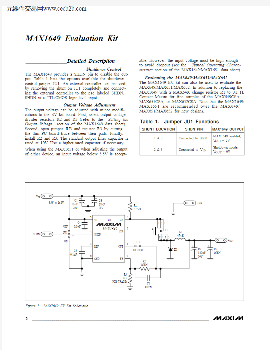
The MAX1649 provides a SHDN pin to disable the out-put. Table 1 lists the options available for shutdown control jumper JU1. An external controller can be used by removing the shunt on JU1 completely and connect-ing the external controller to the pad labeled SHDN.SHDN is a TTL/CMOS logic-level input.
Output Voltage Adjustment
The output voltage can be adjusted with minor modifi-cations to the EV kit board. First, select output voltage divider resistors R2 and R3 (refer to the Setting the Output Voltage section of the MAX1649 data sheet).Second, open jumper JU3 and resistor R3 by cutting the thin PC board trace between their pads. Finally,install R2 and R3. The standard output filter capacitor is rated at 10V. Use a higher-rated capacitor if necessary.When using the MAX1651 or when adjusting the output of either device, an input voltage below 5.5V is accept-
able. However, the input voltage must be high enough to avoid dropout (see the Typical Operating Charac-teristics section of the MAX1649/MAX1651 data sheet).
Evaluating the MAX649/MAX651/MAX652
The MAX1649 EV kit can also be used to evaluate the MAX649/MAX651/MAX652. In addition to replacing the MAX1649 with a MAX649, change resistor R1 to 0.1?.Contact Maxim for free samples of the MAX649CSA,MAX651CSA, or MAX652CSA. Note that the MAX1649/MAX1651 are recommended over the MAX649/MAX651/MAX652 for new designs.
Figure 1. MAX1649 EV Kit Schematic
Evaluates: MAX649/MAX651/MAX652/MAX1649/MAX1651
MAX1649 Evaluation Kit
_______________________________________________________________________________________3
Figure 2. MAX1649 EV Kit Component Placement Guide—Component Side
Figure 3. MAX1649 EV Kit PC Board Layout—Component Side
Figure 4. MAX1649 EV Kit PC Board Layout—Solder Side
E v a l u a t e s : M A X 649/M A X 651/M A X 652/M A X 1649/M A X 1651
MAX1649 Evaluation Kit NOTES
Maxim cannot assume responsibility for use of any circuitry other than circuitry entirely embodied in a Maxim product. No circuit patent licenses are implied. Maxim reserves the right to change the circuitry and specifications without notice at any time.
4_____________________Maxim Integrated Products, 120 San Gabriel Drive, Sunnyvale, CA 94086 408-737-7600?1997 Maxim Integrated Products
Printed USA
is a registered trademark of Maxim Integrated Products.