CY7C68013A-128AXC中文资料
- 格式:pdf
- 大小:1.84 MB
- 文档页数:55
cy7c68013编程方法(最新版4篇)目录(篇1)I.引言A.介绍cy7c68013芯片及其应用领域B.本文将介绍如何对cy7c68011芯片进行编程II.cy7c68013芯片概述A.简介cy7c68013芯片的主要特点B.cy7c68013芯片的应用场景III.cy7c68013编程方法A.编程工具和开发环境介绍B.编程步骤和注意事项C.编程实例IV.总结A.总结cy7c68013编程方法B.展望未来正文(篇1)一、引言随着物联网和智能家居的普及,cy7c68013芯片作为一种低功耗、高性能的微控制器,被广泛应用于各种智能设备中。
本文将介绍如何对cy7c68013芯片进行编程,以实现各种智能控制功能。
二、cy7c68013芯片概述cy7c68013芯片是一款基于ARM Cortex-M3内核的微控制器,具有低功耗、高性能、高集成度等特点。
它支持多种通信接口,如SPI、I2C等,可广泛应用于智能家居、物联网等领域。
三、cy7c68013编程方法1.编程工具和开发环境介绍:使用Keil C51编译环境,下载cy7c68013芯片驱动程序和相关库文件。
2.编程步骤和注意事项:A.编写程序代码,包括初始化时钟、外设等。
B.配置cy7c68013芯片的寄存器,设置中断优先级、GPIO口等功能。
C.编译程序代码,下载到cy7c68013芯片中。
D.进行调试和测试,根据需要进行参数设置和功能扩展。
E.注意事项:i.使用适当的晶振频率,确保系统运行稳定。
ii.注意IO口资源的分配和使用,避免冲突。
iii.注意中断管理,避免中断嵌套导致系统崩溃。
3.编程实例:设计一个基于cy7c68013芯片的智能家居控制系统,实现灯光控制、温度调节等功能。
四、总结本文介绍了如何对cy7c68013芯片进行编程,包括编程工具、开发环境、编程步骤和注意事项等。
通过编程实例,展示了如何将cy7c68013芯片应用于智能家居领域,实现灯光控制、温度调节等功能。
基于FPGA和CY7C68013A的数据采集系统2900字摘要:为了解决计算机和基于FPGA的数据采集系统的数据传输速率的问题,本文设计一种基于CY7C68013A芯片的USB2.0接口方案,设计采用FPGA为主控芯片,实现对USB芯片的控制。
介绍了该系统的硬件设计以及软件工作流程。
实验表明:FPGA通过USB 接口实现了高速可靠的数据传输。
毕业关键词:FPGA;USB2.0;CY7C68013A;数据传输由于USB接口的高速、即插即用,易于扩展等特点其得到广泛应用。
USB2.0高速模式下,数据传输速率可达480Mbps[1-2],是目前电脑中的标准扩展接口。
本系统设计的目的在于基于FPGA控制多路数据采集系统和计算机之间提供一个高速通信接口。
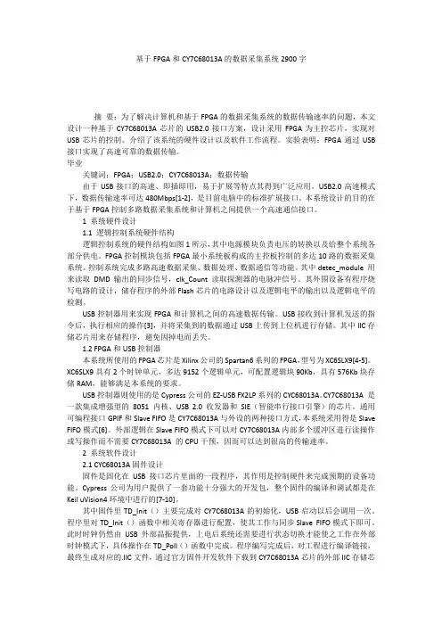
1 系统硬件设计1.1 逻辑控制系统硬件结构逻辑控制系统的硬件结构如图1所示,其中电源模块负责电压的转换以及给整个系统各部分供电。
FPGA控制模块包括FPGA最小系统板构成的主控板控制的多达10路的数据采集系统。
控制系统完成多路高速数据采集、数据处理、数据通信等功能。
其中detec_module 用来读取DMD输出的同步信号,clk_Count 读取探测器的电脉冲信号。
其外围设备有程序烧写电路的设计,储存程序的外部Flash芯片的电路设计以及逻辑电平的输出以及逻辑电平的检测。
USB控制器用来实现FPGA和计算机之间的高速数据传输。
USB接收到计算机发送的指令后,执行相应的操作[3],并将采集到的数据通过USB上传到上位机进行存储。
其中IIC存储芯片用来存储程序,避免因掉电而丢失。
1.2 FPGA和USB控制器本系统所使用的FPGA芯片是Xilinx公司的Spartan6系列的FPGA,型号为XC6SLX9[4-5]。
XC6SLX9具有2个时钟单元,多达9152个逻辑单元,可配置逻辑块90Kb,具有576Kb块存储RAM,能够满足本系统的要求。
USB控制器则使用的是Cypress公司的EZ-USB FX2LP系列的CYC68013A。
USB2.0控制器CY7C68013特点与应用
扈啸;张连起;等
【期刊名称】《单片机与嵌入式系统应用》
【年(卷),期】2002(000)010
【摘要】介绍USB2.0协议以及Cypress公司推出的USB2.0控制器
CY7C680313。
USB2.0协议提供480Mb/s的传输速度,向下完全兼容流行的USB1.1协议。
CY7C68013是USB2.0的完整解决方案,该芯片包括带
8.5KB片上RAM的高速8051单片机,4KB FIFO存储器以及通用可编程接口(GPIF0,串行接口引擎(SIE)和USB2.0收发器,无需外加芯片即可完成高速USB传输,性价比较高。
【总页数】4页(P48-50,54)
【作者】扈啸;张连起;等
【作者单位】长沙国防科学技术大学;长沙国防科学技术大学
【正文语种】中文
【中图分类】TP334.7
【相关文献】
B
2.0微控制器CY7C68013的数据采集系统的设计 [J], 张华洋;周建平;梁楚华
B2.0控制器CY7C68013特点与应用 [J], 扈啸;张玘;张连超
B2.0微控制器CY7C68013与外部FIFO通信发送过程的GPIF接口设计 [J], 白海亮
B2.0控制器CY7C68013在lon总线技术中的应用 [J], 徐进;朱剑雄
B2.0控制器CY7C68013与FPGA接口的Verilog HDL实现 [J], 谭安菊;龚彬
因版权原因,仅展示原文概要,查看原文内容请购买。
基于CY7C68013A芯片的USB键盘的设计陈喜春【期刊名称】《山西电子技术》【年(卷),期】2012(000)001【摘要】Because the characteristics of high transmission speed, small package, and the ability of power supply, the USB inter- face has been widely used in computer peripheral equipment. In this paper, the principle of IC CYTC68013A made by Cypress is discussed, and also it discusses how to design an USB keyboard using CY7C68013A.%由于具备传输速率高、体积小等特点,USB接口广泛地应用于计算机外部硬件设计。
针对此介绍了Cypress 公司的CYTC68013A芯片的基本原理,以及使用CY7C68013A芯片进行USB键盘设计的方法。
【总页数】3页(P6-7,12)【作者】陈喜春【作者单位】石家庄机械化步兵学院军事模拟训练中心,河北石家庄050083【正文语种】中文【中图分类】TP319【相关文献】1.基于MC68HC(9)08JB8芯片的USB产品--键盘设计 [J], 廉德亮;张莹2.基于CY7C68013A的USB2.0高速接口设计 [J], 赵林;孟令军;于磊;张园3.基于CY7C68013A的USB引导启动系统设计和实现 [J], 段建波;杨鸣;吴正管4.基于CY7C68013A的USB通信接口设计 [J], 余亚刚5.基于STM32F103RBT6芯片的USB键盘设计与实现 [J], 张淼;赵冒童因版权原因,仅展示原文概要,查看原文内容请购买。
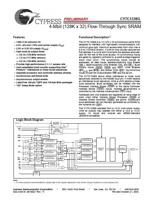
PRELIMINARY4-Mbit (128K x 32) Flow-Through Sync SRAMCY7C1338GFeatures•128K X 32 common I/O•3.3V –5% and +10% core power supply (V DD)•2.5V or 3.3V I/O supply (V DDQ)•Fast clock-to-output times—6.5 ns (133-MHz version)—7.5 ns (117-MHz version)—8.0 ns (100-MHz version)•Provide high-performance 2-1-1-1 access rate •User-selectable burst counter supporting Intel®Pentium® interleaved or linear burst sequences •Separate processor and controller address strobes •Synchronous self-timed write•Asynchronous output enable•Lead-Free 100-pin TQFP and 119-ball BGA packages •“ZZ” Sleep Mode option Functional Description[1]The CY7C1338G is a 131,072 x 32 synchronous cache RAM designed to interface with high-speed microprocessors with minimum glue logic. Maximum access delay from clock rise is 6.5 ns (133-MHz version). A 2-bit on-chip counter captures the first address in a burst and increments the address automati-cally for the rest of the burst access. All synchronous inputs are gated by registers controlled by a positive-edge-triggered Clock Input (CLK). The synchronous inputs include all addresses, all data inputs, address-pipelining Chip Enable (CE1), depth-expansion Chip Enables (CE2 and CE3), Burst Control inputs (ADSC, ADSP, and ADV), Write Enables(BW[A:D], and BWE), and Global Write (GW). Asynchronous i nputs include the Output Enable (OE) and the ZZ pin.The CY7C1338G allows either interleaved or linear burst sequences, selected by the MODE input pin. A HIGH selects an interleaved burst sequence, while a LOW selects a linear burst sequence. Burst accesses can be initiated with the Processor Address Strobe (ADSP) or the cache Controller Address Strobe (ADSC) inputs. Address advancement is controlled by the Address Advancement (ADV) input. Addresses and chip enables are registered at rising edge of clock when either Address Strobe Processor (ADSP) or Address Strobe Controller (ADSC) are active. Subsequent burst addresses can be internally generated as controlled by the Advance pin (ADV).The CY7C1338G operates from a +3.3V core power supply while all outputs may operate with either a +2.5 or +3.3V supply. All inputs and outputs are JEDEC-standard JESD8-5-compatible.Note:1.For best–practices recommendations, please refer to the Cypress application note System Design Guidelines on .Selection Guide133 MHz 117 MHz 100 MHz Unit Maximum Access Time6.57.58.0ns Maximum Operating Current 225220205mA Maximum Standby Current404040mAShaded areas contain advance information. Please contact your local Cypress sales representative for availability of these parts.Pin Configurations100-Pin TQFPAAAAA 1A 0N C N CV S SV D DN C A AAAA ANC DQ B V DDQ V SSQ DQ B DQ B DQ B DQ B V SSQ V DDQ DQ B DQ B V SS NC V DD DQ A DQ A V DDQ V SSQ DQ A DQ A DQ A DQ A V SSQ V DDQ DQ A DQ A NCNC DQ C DQ C V DDQ V SSQ DQ C DQ CDQ C DQ C V SSQ V DDQ DQ C DQ C NC V DD NC V SS DQ D DQ D V DDQ V SSQ DQ D DQ D DQ D DQ D V SSQ V DDQ DQ D DQ D NCAAC E 1C E 2B W DB W CB W BB W AC E 3V D DV S SC L KG WB W EO E A D S P A A123456789101112131415161718192021222324252627282930313233343536373839404142434445464748495080797877767574737271706968676665646362616059585756555453525110099989796959493929190898887868584838281BYTE ABYTE CAA D V A D S C ZZ M O D E N C BYTE BDQ B BYTE DCY7C1338GPin DefinitionsName I/O DescriptionA0, A1, A Input-Synchronous Address Inputs used to select one of the 128K address location s. Sampled at the rising edge of the CLK if ADSP or ADSC is active LOW, and CE1,CE2, and CE3 are sampled active. A[1:0] feed the 2-bit counter.BW A,BW B BW C,BW DInput-SynchronousByte Write Select Inputs, active LOW. Qualified with BWE to conduct byte writes to the SRAM.Sampled on the rising edge of CLK.GW Input-Synchronous Global Write Enable Input, active LOW. When asserted LOW on the rising edge of CLK, a global write is conducted (ALL bytes are written, regardless of the values on BW[A:D] and BWE).BWE Input-Synchronous Byte Write Enable Input, active LOW. Sampled on the rising edge of CLK. This signal must be asserted LOW to conduct a byte write.CLK Input-Clock Clock Input. Used to capture all synchronous inputs to the device. Also used to increment the burst counter when ADV is asserted LOW, during a burst operation.CE1Input-Synchronous Chip Enable 1 Input, active LOW. Sampled on the rising edge of CLK. Used in conjunction with CE2 and CE3 to select/deselect the device. ADSP is ignored if CE1 is HIGH.CE1 is sampled only when a new external address is loaded.CE2Input-Synchronous Chip Enable 2 Input, active HIGH. Sampled on the rising edge of CLK. Used in conjunction with CE1 and CE3 to select/deselect the device. CE2 is sampled only when a new external address is loaded.CE3Input-Synchronous Chip Enable 3 Input, active LOW. Sampled on the rising edge of CLK. Used in conjunction with CE1 and CE2 to select/deselect the device. CE3 is sampled only when a new external address is loaded.OE Input-Asynchronous Output Enable, asynchronous input, active LOW. Controls the direction of the I/O pins. When LOW, the I/O pins behave as outputs. When deasserted HIGH, I/O pins are tri-stated, and act as input data pins. OE is masked during the first clock of a read cycle when emerging from a deselected state.ADV Input-Synchronous Advance Input signal, sampled on the rising edge of CLK. When asserted, it automatically increments the address in a burst cycle.Pin Configurations (continued)2345671A B C D E F G H J K L M N P R T U V DDQNCNCNCDQ CDQ DDQ CDQ DA A A AADSP V DDQ CE2ADQ CV DDQDQ CV DDQV DDQV DDQDQ DDQ DNCNCV DDQV DDCLKV DDV SSV SSV SSV SSV SSV SSV SSV SSNCNCNCNCNCNCNCNCNCNCNCV DDQV DDQV DDQA A AANCAAAAAAA0A1DQ A DQ CDQ ADQ ADQ ADQ BDQ BDQ BDQ BDQ BDQ BDQ BDQ ADQ ADQ ADQ ADQ BV DDDQ CDQ CDQ CV DDDQ DDQ DDQ DDQ DADSCNCCE1OEADVGWV SSV SSV SSV SSV SSV SSV SSV SS NCMODENCNCBW BBW CNC V DD NCBW ANCBWEBW DZZ119-Ball BGAFunctional OverviewAll synchronous inputs pass through input registers controlled by the rising edge of the clock. Maximum access delay from the clock rise (t C0) is 6.5 ns (133-MHz device).The CY7C1338G supports secondary cache in systems utilizing either a linear or interleaved burst sequence. The interleaved burst order supports Pentium ® and i486™processors. The linear burst sequence is suited for processors that utilize a linear burst sequence. The burst order is user-selectable, and is determined by sampling the MODE input. Accesses can be initiated with either the Processor Address Strobe (ADSP) or the Controller Address Strobe (ADSC). Address advancement through the burst sequence is controlled by the ADV input. A two-bit on-chip wraparound burst counter captures the first address in a burst sequence and automatically increments the address for the rest of the burst access.Byte write operations are qualified with the Byte Write Enable (BWE) and Byte Write Select (BW [A:D]) inputs. A Global Write Enable (GW) overrides all byte write inputs and writes data to all four bytes. All writes are simplified with on-chip synchronous self-timed write circuitry.Three synchronous Chip Selects (CE 1, CE 2, CE 3) and an asynchronous Output Enable (OE) provide for easy bank selection and output tri-state control. ADSP is ignored if CE 1is HIGH.Single Read AccessesA single read access is initiated when the following conditions are satisfied at clock rise: (1) CE 1, CE 2, and CE 3 are all asserted active, and (2) ADSP or ADSC is asserted LOW (if the access is initiated by ADSC, the write inputs must be deasserted during this first cycle). The address presented to the address inputs is latched into the address register and the burst counter/control logic and presented to the memory core.If the OE input is asserted LOW, the requested data will be available at the data outputs a maximum to t CDV after clock rise. ADSP is ignored if CE 1 is HIGH.Single Write Accesses Initiated by ADSPThis access is initiated when the following conditions are satisfied at clock rise: (1) CE 1, CE 2, CE 3 are all asserted active, and (2) ADSP is asserted LOW. The addresses presented are loaded into the address register and the burst inputs (GW, BWE, and BW[A:D ])are ignored during this first clock cycle. If the write inputs are asserted active (see Write Cycle Descriptions table for appropriate states that indicate a write) on the next clock rise, the appropriate data will be latched and written into the device. Byte writes are allowed.During byte writes, BW A controls DQ A and BWB controls DQ B .BWC controls DQ C , and BW D controls DQ D . All I/Os are tri-stated during a byte write.Since this is a common I/O device, the asynchronous OE input signal must be deasserted and the I/Os must be tri-stated prior to the presentation of data to DQs. As a safety precaution, the data lines are tri-stated once a write cycle is detected, regardless of the state of OE.ADSPInput-Synchronous Address Strobe from Processor, sampled on the rising edge of CLK, active LOW . Whenasserted LOW, addresses presented to the device are captured in the address registers. A [1:0] arealso loaded into the burst counter. When ADSP and ADSC are both asserted, only ADSP is recog-nized. ASDP is ignored when CE 1 is deasserted HIGHADSC Input-Synchronous Address Strobe from Controller, sampled on the rising edge of CLK, active LOW . When assertedLOW, addresses presented to the device are captured in the address registers. A [1:0] are also loadedinto the burst counter. When ADSP and ADSC are both asserted, only ADSP is recognized.ZZInput-Asynchronous ZZ “sleep” Input, active HIGH . When asserted HIGH places the device in a non-time-critical “sleep”condition with data integrity preserved. For normal operation, this pin has to be LOW or left floating.ZZ pin has an internal pull-down.DQsI/O-Synchronous Bidirectional Data I/O lines . As inputs, they feed into an on-chip data register that is triggered bythe rising edge of CLK. As outputs, they deliver the data contained in the memory location specifiedby the addresses presented during the previous clock rise of the read cycle. The direction of the pins is controlled by OE . When OE is asserted LOW, the pins behave as outputs. When HIGH, DQs are placed in a tri-state condition.V DD Power Supply Power supply inputs to the core of the device .V SS GroundGround for the core of the device .V DDQ I/O Power SupplyPower supply for the I/O circuitry . V SSQ I/O Ground Ground for the I/O circuitry . MODEInput-StaticSelects Burst Order . When tied to GND selects linear burst sequence. When tied to V DD or left floating selects interleaved burst sequence. This is a strap pin and should remain static during device operation. Mode Pin has an internal pull-up.NCNo Connects . Not Internally connected to the die.Pin Definitions (continued)Name I/ODescriptionSingle Write Accesses Initiated by ADSCThis write access is initiated when the following conditions are satisfied at clock rise: (1) CE1, CE2, and CE3 are all asserted active, (2) ADSC is asserted LOW, (3) ADSP is deasserted HIGH, and (4) the write input signals (GW, BWE, and BW[A:D]) indicate a write access. ADSC is ignored if ADSP is active LOW.The addresses presented are loaded into the address register and the burst counter/control logic and delivered to the memory core. The information presented to DQ[A:D] will be written into the specified address location. Byte writes are allowed. During byte writes, BW A controls DQ A, BW B controls DQ B, BW C controls DQ C, and BW D controls DQ D. All I/Os are tri-stated when a write is detected, even a byte write. Since this is a common I/O device, the asynchronous OE input signal must be deasserted and the I/Os must be tri-stated prior to the presentation of data to DQs. As a safety precaution, the data lines are tri-stated once a write cycle is detected, regardless of the state of OE.Burst SequencesThe CY7C1338G provides an on-chip two-bit wraparound burst counter inside the SRAM. The burst counter is fed by A[1:0], and can follow either a linear or interleaved burst order. The burst order is determined by the state of the MODE input.A LOW on MODE will select a linear burst sequence. A HIGH on MODE will select an interleaved burst order. Leaving MODE unconnected will cause the device to default to a inter-leaved burst sequence.Sleep ModeThe ZZ input pin is an asynchronous input. Asserting ZZ places the SRAM in a power conservation “sleep” mode. Two clock cycles are required to enter into or exit from this “sleep”mode. While in this mode, data integrity is guaranteed. Accesses pending when entering the “sleep” mode are not considered valid nor is the completion of the operation guaranteed. The device must be deselected prior to entering the “sleep” mode. CEs, ADSP, and ADSC must remain inactive for the duration of t ZZREC after the ZZ input returns LOW.Interleaved Burst Address Table(MODE = Floating or V DD)FirstAddressA1, A0SecondAddressA1, A0ThirdAddressA1, A0FourthAddressA1, A0 00011011010011101011000111100100 Linear Burst Address Table (MODE = GND) FirstAddressA1,A0SecondAddressA1,A0ThirdAddressA1,A0FourthAddressA1,A0 00011011011011001011000111000110ZZ Mode Electrical CharacteristicsParameter Description Test Conditions Min.Max.Unit I DDZZ Snooze mode standby current ZZ > V DD– 0.2V40mA t ZZS Device operation to ZZ ZZ > V DD – 0.2V2t CYC ns t ZZREC ZZ recovery time ZZ < 0.2V2t CYC ns t ZZI ZZ active to snooze current This parameter is sampled2t CYC ns t RZZI ZZ Inactive to exit snooze current This parameter is sampled0nsTruth Table[2, 3, 4, 5, 6]Cycle Description AddressUsed CE1CE2CE3ZZ ADSP ADSC ADV WRITE OE CLK DQDeselected Cycle, Power-down None H X X L X L X X X L-H tri-state Deselected Cycle, Power-down None L L X L L X X X X L-H tri-state Deselected Cycle, Power-down None L X H L L X X X X L-H tri-state Deselected Cycle, Power-down None L L X L H L X X X L-H tri-state Deselected Cycle, Power-down None X X X L H L X X X L-H tri-state Snooze Mode, Power-down None X X X H X X X X X X tri-state Read Cycle, Begin Burst External L H L L L X X X L L-H QRead Cycle, Begin Burst External L H L L L X X X H L-H tri-state Write Cycle, Begin Burst External L H L L H L X L X L-H DRead Cycle, Begin Burst External L H L L H L X H L L-H QRead Cycle, Begin Burst External L H L L H L X H H L-H tri-state Read Cycle, Continue Burst Next X X X L H H L H L L-H QRead Cycle, Continue Burst Next X X X L H H L H H L-H tri-state Read Cycle, Continue Burst Next H X X L X H L H L L-H QRead Cycle, Continue Burst Next H X X L X H L H H L-H tri-state Write Cycle, Continue Burst Next X X X L H H L L X L-H DWrite Cycle, Continue Burst Next H X X L X H L L X L-H DRead Cycle, Suspend Burst Current X X X L H H H H L L-H QRead Cycle, Suspend Burst Current X X X L H H H H H L-H tri-state Read Cycle, Suspend Burst Current H X X L X H H H L L-H QRead Cycle, Suspend Burst Current H X X L X H H H H L-H tri-state Write Cycle, Suspend Burst Current X X X L H H H L X L-H DWrite Cycle, Suspend Burst Current H X X L X H H L X L-H D Notes:2.X = “Don't Care.” H = Logic HIGH, L = Logic LOW.3.WRITE = L when any one or more Byte Write enable signals (BW A, BW B, BW C, BW D) and BWE = L or GW= L. WRITE = H when all Byte write enable signalsA B C D4.The DQ pins are controlled by the current cycle and the OE signal. OE is asynchronous and is not sampled with the clock.5.The SRAM always initiates a read cycle when ADSP is asserted, regardless of the state of GW, BWE, or BW X. Writes may occur only on subsequent clocksafter the or with the assertion of ADSC. As a result, OE must be driven HIGH prior to the start of the write cycle to allow the outputs to tri-state. OE is a don't care for the remainder of the write cycle.6.OE is asynchronous and is not sampled with the clock rise. It is masked internally during write cycles. During a read cycle all data bits are tri-state when OE isinactive or when the device is deselected, and all data bits behave as output when OE is active (LOW).Partial Truth Table for Read/Write[2, 7]Function GW BWE BW D BW C BW B BW A Read H H X X X X Read H L H H H H Write Byte A H L H H H L Write Byte B H L H H L H Write Bytes B, A H L H H L L Write Byte C H L H L H H Write Bytes C, A H L H L H L Write Bytes C, B H L H L L H Write Bytes C, B, A H L H L L L Write Byte D H L L H H H Write Bytes D, A H L L H H L Write Bytes D, B H L L H L H Write Bytes D, B, A H L L H L L Write Bytes D, B H L L L H H Write Bytes D, B, A H L L L H L Write Bytes D,C,A H L L L L H Write All Bytes H L L L L L Write All Bytes L X X X X X Note:7.Table only lists a partial listing of the byte write combinations. Any combination of BW X is valid. Appropriate write will be done based on which byte write is active.Maximum Ratings(Above which the useful life may be impaired. For user guide-lines, not tested.)Storage Temperature .................................–65°C to +150°C Ambient Temperature withPower Applied.............................................–55°C to +125°C Supply Voltage on V DD Relative to GND........–0.5V to +4.6V DC Voltage Applied to Outputsin tri-state............................................–0.5V to V DDQ + 0.5V DC Input Voltage....................................–0.5V to V DD + 0.5V Current into Outputs (LOW).........................................20 mA Static Discharge Voltage........................................... >2001V (per MIL-STD-883, Method 3015)Latch-up Current..................................................... >200 mA Operating RangeRangeAmbientTemperature]V DD V DDQ Commercial0°C to +70°C 3.3V −5%/+10% 2.5V –5%to V DD Industrial–40°C to +85°CElectrical Characteristics Over the Operating Range[8, 9]Parameter Description Test ConditionsCY7C1338GUnit Min.Max.V DD Power Supply Voltage 3.135 3.6V V DDQ I/O Supply Voltage 2.375V DD V V OH Output HIGH Voltage V DDQ = 3.3V, V DD = Min., I OH = –4.0 mA 2.4VV DDQ = 2.5V, V DD = Min., I OH = –1.0 mA 2.0V V OL Output LOW Voltage V DDQ = 3.3V, V DD = Min., I OL = 8.0 mA0.4VV DDQ = 2.5V, V DD = Min., I OL = 1.0 mA0.4V V IH Input HIGH Voltage V DDQ = 3.3V 2.0V DD + 0.3V VV DDQ = 2.5V 1.7V DD + 0.3V V V IL Input LOW Voltage[8]V DDQ = 3.3V–0.30.8VV DDQ = 2.5V–0.30.7V I X Input Load Current (except ZZ andMODE)GND ≤ V I≤ V DDQ−55µA Input Current of MODE Input = V SS–30µAInput = V DD5µA Input Current of ZZ Input = V SS–5µAInput = V DD30µA I OZ Output Leakage Current GND ≤ V I≤ V DD, Output Disabled–55µA I OS Output Short Circuit Current V DD = Max., V OUT = GND–300µAI DD V DD Operating Supply Current V DD = Max., I OUT = 0 mA,f = f MAX= 1/t CYC 7.5-ns cycle, 133 MHz225mA8.0-ns cycle, 117 MHz220mA 10-ns cycle, 100 MHz205mAI SB1Automatic CE Power-DownCurrent—TTL Inputs Max. V DD, Device Deselected,V IN≥ V IH or V IN≤ V IL, f = f MAX,inputs switching7.5-ns cycle, 133 MHz90mA8.0-ns cycle, 117 MHz85mA10-ns cycle, 100 MHz80mAI SB2Automatic CE Power-DownCurrent—CMOS Inputs Max. V DD, Device Deselected,V IN≥ V DD – 0.3V or V IN≤ 0.3V,f = 0, inputs staticAll speeds40mAI SB3Automatic CE Power-DownCurrent—CMOS Inputs Max. V DD, Device Deselected,V IN≥V DDQ – 0.3V or V IN≤ 0.3V,f = f MAX, inputs switching7.5-ns cycle, 133 MHz75mA8.0-ns cycle, 117 MHz70mA10-ns cycle, 100 MHz65mAI SB4Automatic CE Power-DownCurrent—TTL Inputs Max. V DD, Device Deselected,V IN≥ V DD – 0.3V or V IN≤ 0.3V,f=0, inputs staticAll speeds45mAShaded areas contain advance information.Notes:8.Overshoot: V IH(AC) < V DD +1.5V (Pulse width less than t CYC/2), undershoot: V IL(AC) > -2V (Pulse width less than t CYC/2).9.TPower-up: Assumes a linear ramp from 0v to V DD(min.) within 200ms. During this time V IH < V DD and V DDQ < V DD.Thermal Resistance [10]Parameter DescriptionTest ConditionsTQFP PackageBGA PackageUnit ΘJAThermal Resistance (Junction to Ambient)Test conditions follow standard test methods and procedures formeasuring thermal impedance, per EIA / JESD51.TBD TBD °C/W ΘJC Thermal Resistance(Junction to Case)TBDTBD°C/WCapacitance [10]Parameter DescriptionTest Conditions TQFP PackageBGA Package UnitC IN Input Capacitance T A = 25°C, f = 1 MHz,V DD = 3.3V. V DDQ = 3.3V55pF C CLK Clock Input Capacitance 55pF C I/OInput/Output Capacitance57pFAC Test Loads and WaveformsSwitching Characteristics Over the Operating Range [11, 12, 13, 14, 15, 16]Parameter Description133 MHz117 MHz 100 MHz Unit Min.Max.Min.Max.Min.Max.t POWER V DD (Typical) to the first Access [11]111msClock t CYC Clock Cycle Time 7.58.510ns t CH Clock HIGH 2.5 3.0 4.0ns t CLClock LOW2.53.04.0nsOutput Times t CDV Data Output Valid After CLK Rise 6.57.58.0ns t DOHData Output Hold After CLK Rise2.02.02.0nsShaded areas contain advance information.Notes:10.Tested initially and after any design or process change that may affect these parameters.11.This part has a voltage regulator internally; t POWER is the time that the power needs to be supplied above V DD (minimum) initially before a read or write operationcan be initiated.12.t CHZ , t CLZ ,t OELZ , and t OEHZ are specified with AC test conditions shown in part (b) of AC Test Loads. Transition is measured ± 200 mV from steady-state voltage.13.At any given voltage and temperature, t OEHZ is less than t OELZ and t CHZ is less than t CLZ to eliminate bus contention between SRAMs when sharing the samedata bus. These specifications do not imply a bus contention condition, but reflect parameters guaranteed over worst case user conditions. Device is designed to achieve High-Z prior to Low-Z under the same system conditions.14.This parameter is sampled and not 100% tested.15.Timing reference level is 1.5V when V DDQ = 3.3V and is 1.25V when V DDQ = 2.5V.16.Test conditions shown in (a) of AC Test Loads unless otherwise noted.OUTPUTR = 317ΩR = 351Ω5pFINCLUDING JIG AND SCOPE (a)(b)OUTPUTR L = 50ΩZ 0= 50ΩV T = 1.5V3.3VALL INPUT PULSESV DDQ GND90%10%90%10%≤1ns≤1ns(c)OUTPUTR = 1667ΩR =1538Ω5pFINCLUDING JIG AND SCOPE(a)(b)OUTPUTR L = 50ΩZ 0= 50ΩV T = 1.25V2.5VALL INPUT PULSES V DDQGND90%10%90%10%≤1ns≤1ns(c)3.3V I/O Test Load2.5V I/O Test Loadt CLZ Clock to Low-Z [12, 13, 14]0ns t CHZ Clock to High-Z [12, 13, 14] 3.5 3.5 3.5ns t OEV OE LOW to Output Valid3.53.5 3.5ns t OELZ OE LOW to Output Low-Z [12, 13, 14]0ns t OEHZOE HIGH to Output High-Z [12, 13, 14]3.53.53.5ns Setup Times t AS Address Set-up Before CLK Rise 1.5 2.0 2.0ns t ADS ADSP , ADSC Set-up Before CLK Rise 1.5 2.0 2.0ns t ADVS ADV Set-up Before CLK Rise1.52.0 2.0ns t WES GW, BWE, BW X Set-up Before CLK Rise 1.5 2.0 2.0ns t DS Data Input Set-up Before CLK Rise 1.5 1.5 1.5ns t CESChip Enable Set-up1.52.02.0ns Hold Times t AH Address Hold After CLK Rise 0.50.50.5ns t ADH ADSP , ADSC Hold After CLK Rise 0.50.50.5ns t WEH GW ,BWE , BW X Hold After CLK Rise 0.50.50.5ns t ADVH ADV Hold After CLK Rise 0.50.50.5ns t DH Data Input Hold After CLK Rise 0.50.50.5ns t CEHChip Enable Hold After CLK Rise0.50.50.5nsSwitching Characteristics Over the Operating Range (continued)[11, 12, 13, 14, 15, 16]Parameter Description133 MHz117 MHz 100 MHz Unit Min.Max.Min.Max.Min.Max.Timing Diagrams[17]Timing Diagrams (continued)[17, 18]Timing Diagrams (continued)[17, 19, 20]ZZ Mode Timing [21, 22]Ordering InformationSpeed (MHz)Ordering Code Package Name Package TypeOperating Range 133CY7C1338G-133AXC A101Lead-Free 100-Lead Thin Quad Flat Pack (14 x 20 x 1.4mm)CommercialCY7C1338G-133BGC BG119119-Ball PBGA (14 x 22 x 2.4mm)CY7C1338G-133BGXC BG119Lead-Free 119-Ball PBGA (14 x 22 x 2.4mm)CY7C1338G-133AXI A101Lead-Free 100-Lead Thin Quad Flat Pack (14 x 20 x 1.4mm)Industrial CY7C1338G-133BGI BG119119-Ball PBGA (14 x 22 x 2.4mm)CY7C1338G-133BGXIBG119Lead-Free 119-Ball PBGA (14 x 22 x 2.4mm)117CY7C1338G-117AXC A101Lead-Free 100-Lead Thin Quad Flat Pack (14 x 20 x 1.4mm)Commercial CY7C1338G-117BGC BG119119-Ball PBGA (14 x 22 x 2.4mm)CY7C1338G-117BGXCBG119Lead-Free 119-Ball PBGA (14 x 22 x 2.4mm)CY7C1338G-117AXI A101Lead-Free 100-Lead Thin Quad Flat Pack (14 x 20 x 1.4mm)Industrial CY7C1338G-117BGI BG119119-Ball PBGA (14 x 22 x 2.4mm)CY7C1338G-117BGXIBG119Lead-Free 119-Ball PBGA (14 x 22 x 2.4mm)100CY7C1338G-100AXC A101Lead-Free 100-Lead Thin Quad Flat Pack (14 x 20 x 1.4mm)Commercial CY7C1338G-100BGC BG119119-Ball PBGA (14 x 22 x 2.4mm)CY7C1338G-100BGXC BG119Lead-Free 119-Ball PBGA (14 x 22 x 2.4mm)CY7C1338G-100AXI A101Lead-Free 100-Lead Thin Quad Flat Pack (14 x 20 x 1.4mm)Industrial CY7C1338G-100BGI BG119119-Ball PBGA (14 x 22 x 2.4mm)CY7C1338G-100BGXIBG119Lead-Free 119-Ball PBGA (14 x 22 x 2.4mm)Shaded areas contain advance information. Please contact your local Cypress sales representative for availability of these parts. Lead-Free BGX package will be available in 2005.Notes:21.Device must be deselected when entering ZZ mode. See Cycle Descriptions table for all possible signal conditions to deselect the device.22.DQs are in high-Z when exiting ZZ sleep mode.Timing Diagrams (continued)Package DiagramsDocument #: 38-05521 Rev. *A Page 16 of 17Intel and Pentium are registered trademarks of Intel Corporation. All product and company names mentioned in this document may be the trademarks of their respective holders.Package Diagrams(continued)Document History PageDocument Title: CY7C1338G 4-Mbit (128K x 32) Flow-Through Sync SRAM Document Number: 38-05521REV.ECN NO.Issue Date Orig. ofChange Description of Change**224369See ECN RKF New data sheet*A278513See ECN VBL Deleted 66 MHzChanged TQFP to PB-Free TQFP in Ordering Info sectionAdded PB-Free BG package。
CY7C68013EZ-USB® FX2™ USB MicrocontrollerHigh-Speed USB Peripheral ControllerTABLE OF CONTENTS1.0 EZ-USB® FX2™ FEATURES (6)2.0 APPLICATIONS (7)3.0 FUNCTIONAL OVERVIEW (7)3.1 USB Signaling Speed (7)3.2 8051 Microprocessor (7)3.3 I2C-compatible Bus (8)3.4 Buses (8)3.5 USB Boot Methods (9)3.6 ReNumeration™ (9)3.7 Interrupt System (9)3.8 Reset and Wakeup (11)3.9 Program/Data RAM (11)3.10 Register Addresses (14)3.11 Endpoint RAM (14)3.12 External FIFO interface (16)3.13 GPIF (16)3.14 USB Uploads and Downloads (17)3.15 Autopointer Access (17)3.16 I2C-compatible Controller (17)4.0 PIN ASSIGNMENTS (18)4.1 CY7C68013 Pin Descriptions (23)5.0 REGISTER SUMMARY (30)6.0 ABSOLUTE MAXIMUM RATINGS (36)7.0 OPERATING CONDITIONS (36)8.0 DC CHARACTERISTICS (36)9.0 AC ELECTRICAL CHARACTERISTICS (37)9.1 USB Transceiver (37)9.2 Program Memory Read (37)9.3 Data Memory Read (38)9.4 Data Memory Write (39)9.5 GPIF Synchronous Signals (40)9.6 Slave FIFO Synchronous Read (41)9.7 Slave FIFO Asynchronous Read (42)9.8 Slave FIFO Synchronous Write (42)9.9 Slave FIFO Asynchronous Write (43)9.10 Slave FIFO Synchronous Packet End Strobe (43)9.11 Slave FIFO Asynchronous Packet End Strobe (44)9.12 Slave FIFO Output Enable (44)9.13 Slave FIFO Address to Flags/Data (44)9.14 Slave FIFO Synchronous Address (45)9.15 Slave FIFO Asynchronous Address (45)10.0 ORDERING INFORMATION (45)11.0 PACKAGE DIAGRAMS (46)LIST OF FIGURESFigure 1-1. Block Diagram (5)Figure 3-1. Internal Code Memory, EA = 0 (11)Figure 3-2. External Code Memory, EA = 1 (12)Figure 3-3. Endpoint Configuration (14)Figure 4-1. Signals (18)Figure 4-2. CY7C68013 128-pin TQFP Pin Assignment (19)Figure 4-3. CY7C68013 100-pin TQFP Pin Assignment (20)Figure 4-4. CY7C68013 56-pin SSOP Pin Assignment (21)Figure 9-1. Program Memory Read Timing Diagram (36)Figure 9-2. Data Memory Read Timing Diagram (37)Figure 9-3. Data Memory Write Timing Diagram (38)Figure 9-4. GPIF Synchronous Signals Timing Diagram[12] (39)Figure 9-5. Slave FIFO Synchronous Read Timing Diagram[12] (40)Figure 9-6. Slave FIFO Asynchronous Read Timing Diagram[12] (41)Figure 9-7. Slave FIFO Synchronous Write Timing Diagram[12] (41)Figure 9-8. Slave FIFO Asynchronous Write Timing Diagram[12] (42)Figure 9-9. Slave FIFO Synchronous Packet End Strobe Timing Diagram[12] (42)Figure 9-10. Slave FIFO Asynchronous Packet End Strobe Timing Diagram[12] (43)Figure 9-11. Slave FIFO Output Enable Timing Diagram[12] (43)Figure 9-12. Slave FIFO Address to Flags/Data Timing Diagram[12] (43)Figure 9-13. Slave FIFO Synchronous Address Timing Diagram (44)Figure 9-14. Slave FIFO Asynchronous Address Timing Diagram[12] (44)Figure 11-1. 56-lead Shrunk Small Outline Package O56 (45)Figure 11-2. 100-Pin Thin Plastic Quad Flatpack (14 x 20 x 1.4 mm) A101 (46)Figure 11-3. 128-Lead Thin Plastic Quad Flatpack (14 x 20 x 1.4 mm) A128 (47)LIST OF TABLESTable 3-1. Default ID Values for FX2 (8)Table 3-2. INT2 USB Interrupts (9)Table 3-3. Individual FIFO/GPIF Interrupt Sources (10)Table 3-4. Default Full-Speed Alternate Settings[1, 2] (14)Table 3-5. Default High-Speed Alternate Settings[1, 2] (15)Table 3-6. Strap Boot EEPROM Address Lines to These Values (17)Table 4-1. FX2 Pin Descriptions[5] (22)Table 5-1. FX2 Register Summary (29)Table 8-1. DC Characteristics (35)Table 8-2. USB Transceiver (35)Table 9-1. Program Memory Read Parameters (36)Table 9-2. Data Memory Read Parameters (37)Table 9-3. Data Memory Write Parameters (38)Table 9-4. GPIF Synchronous Signals Parameters with Internally Sourced IFCLK[13, 14] (39)Table 9-5. GPIF Synchronous Signals Parameters with Externally Sourced IFCLK[14] (39)Table 9-6. Slave FIFO Synchronous Read Parameters with Internally Sourced IFCLK[14] (40)Table 9-7. Slave FIFO Synchronous Read Parameters with Externally Sourced IFCLK[14] (40)Table 9-8. Slave FIFO Asynchronous Read Parameters[15] (41)Table 9-9. Slave FIFO Synchronous Write Parameters with Internally Sourced IFCLK [14] (41)Table 9-10. Slave FIFO Synchronous Write Parameters with Externally Sourced IFCLK [14] (42)Table 9-11. Slave FIFO Asynchronous Write Parameters with Internally Sourced IFCLK [15] (42)Table 9-12. Slave FIFO Synchronous Packet End Strobe Parameterswith Internally Sourced IFCLK [14] (42)Table 9-13. Slave FIFO Synchronous Packet End Strobe Parameterswith Externally Sourced IFCLK [14] (43)Table 9-14. Slave FIFO Asynchronous Packet End Strobe Parameters[15] (43)Table 9-15. Slave FIFO Output Enable Parameters (43)Table 9-16. Slave FIFO Address to Flags/Data Parameters (44)Table 9-17. Slave FIFO Synchronous Address Parameters [14] (44)Table 9-18. Slave FIFO Asynchronous Address Parameters[15] (44)Table 10-1. Ordering Information (44)1.0EZ-USB ® FX2™ FeaturesCypress’s EZ-USB ® FX2™ is the world ’s first USB 2.0 integrated microcontroller. By integrating the USB 2.0 transceiver, SIE,enhanced 8051 microcontroller, and a programmable peripheral interface in a single chip, Cypress has created a very cost-effective solution that provides superior time-to-market advantages. The ingenious architecture of FX2 results in data transfer rates of 56 Mbytes per second, the maximum allowable USB 2.0 bandwidth, while still using a low-cost 8051 microcontroller in a package as small as a 56 SSOP . Because it incorporates the USB 2.0 transceiver, the FX2 is more economical, providing a smaller footprint solution than USB 2.0 SIE or external transceiver implementations. With EZ-USB FX2, the Cypress Smart SIE handles most of the USB 1.1 and 2.0 protocol in hardware, freeing the embedded microcontroller for application-specific functions and decreasing development time to ensure USB compatibility. The General Programmable Interface (GPIF) and Master/Slave Endpoint FIFO (8- or 16-bit data bus) provides an easy and glueless interface to popular interfaces such as ATA, UTOPIA, EPP ,PCMCIA, and most DSP/processors.Three packages are defined for the family: 56 SSOP , 100 TQFP , and 128 TQFP .•Single-chip integrated USB 2.0 Transceiver, Serial Interface Engine (SIE), and Enhanced 8051 Microprocessor •Software: 8051 runs from internal RAM, which is:—Downloaded via USB, or —Loaded from EEPROM—External memory device (128-pin configuration only)•Four programmable BULK/INTERRUPT/ISOCHRONOUS endpoints —Buffering options: double, triple and quad •8- or 16-bit external data interface•General Programmable Interface (GPIF)—Allows direct connection to most parallel interfaces; 8- and 16-bit—Programmable waveform descriptors and configuration registers to define waveforms —Supports multiple Ready (RDY) inputs and Control (CTL) outputs •Integrated, industry standard 8051 with enhanced features:—Up to 48-MHz clock rate —Four clocks per instruction cycle —Two USARTSA d d r e s s (16)x20PLL/0.5/1.0/2.08051 Core 12/24/48 MHz,four clocks/cycleI 2C Compatible V CC1.5kD+D –A d d r e s s (16) / D a t aB u s (8)FX2GPIFCY Smart USB 1.1/2.0EngineUSB 2.0XCVR8.5 kB RAM4 kB FIFOIntegrated full- and high-speedXCVRAdditional I/Os (24)ADDR (9)CTL (6)RDY (6)8/16D a t a (8)24 MHz Ext. XTALEnhanced USB core Simplifies 8051 core “Soft Configuration ”Easy firmware changes FIFO and endpoint memory (master or slave operation)Up to 96 MBytes/s burst rateGeneralprogrammable I/F to ASIC/DSP or bus standards such as ATAPI, EPP, etc.Abundant I/Oincluding two USARTS High-performance micro using standard toolswith lower-power optionsMasterFigure 1-1. Block Diagramconnected for full speed—Three counter/timers—Expanded interrupt system—Two data pointers•3.3V operation•Smart Serial Interface Engine•Vectored USB interrupts•Separate data buffers for the SETUP and DATA portions of a CONTROL transfer•Integrated I2C-compatible controller, runs at 100 or 400 kHz•48-MHz, 24-MHz, or 12-MHz 8051 operation•Four integrated FIFOs—Brings glue and FIFOs inside for lower system cost—Automatic conversion to and from 16-bit buses—Master or slave operation—FIFOs can use externally supplied clock or asynchronous strobes—Easy interface to ASIC and DSP ICs•Special autovectors for FIFO and GPIF interrupts•Up to 40 general purpose I/Os•Three package options—128-pin TQFP, 100-pin TQFP, and 56-pin SSOP.2.0 Applications•DSL modems•ATA interface•Memory card readers•Legacy conversion devices•Cameras•Scanners•Home PNA•Wireless LAN•MP3 players•Networking.The “Reference Designs” section of the cypress website provides additional tools for typical USB 2.0 applications. Each reference design comes complete with firmware source and object code, schematics, and documentation. Please visit /usb for more information.3.0 Functional Overview3.1USB Signaling SpeedFX2 operates at two of the three rates defined in the Universal Serial Bus Specification Revision 2.0, dated April 27, 2000:•Full speed, with a signaling bit rate of 12 Mbps•High speed, with a signaling bit rate of 480 MbpsFX2 does not support the low-speed signaling mode of 1.5 Mbps.3.28051 MicroprocessorThe 8051 microprocessor embedded in the FX2 family has 256 bytes of register RAM, an expanded interrupt system, three timer/counters, and two USARTs.3.2.18051 Clock FrequencyFX2 has an on-chip oscillator circuit that uses an external 24-MHz (±100 ppm) crystal with the following characteristics:•Parallel resonant•Fundamental mode•500 µW drive level•27–33 pF (5% tolerance) load capacitors.An on-chip PLL multiplies the 24-MHz oscillator up to 480 MHz, as required by the transceiver/PHY, and internal counters divide it down for use as the 8051 clock. The default 8051 clock frequency is 12 MHz. The clock frequency of the 8051 can be changed by the 8051 through the CPUCS register, dynamically.The CLKOUT pin, which can be three-stated and inverted using internal control bits, outputs the 50% duty cycle 8051 clock, at the selected 8051 clock frequency—48, 24, or 12 MHz.3.2.2USARTSFX2 contains two standard 8051 USARTs, addressed via Special Function Register (SFR) bits. The USART interface pins are available on separate I/O pins, and are not multiplexed with port pins.UART0 and UART1 can operate using an internal clock at 230 KBaud with no more than 1% baud rate error. 230-KBaud operation is achieved by an internally derived clock source that generates overflow pulses at the appropriate time. The internal clock adjusts for the 8051 clock rate (48, 24, 12 MHz) such that it always presents the correct frequency for 230-KBaud operation.Note. 115-KBaud operation is also possible by programming the 8051 SMOD0 or SMOD1 bits to a “1” for UART0 and/or UART1, respectively.3.2.3Special Function Registers (SFR)Certain 8051 SFR addresses are populated to provide fast access to critical FX2 functions. These SFR additions are shown in Table 3-1. Bold type indicates non-standard, enhanced 8051 registers.The two SFR rows that end with “0” and “8” contain bit-addressable registers. The four I/O ports A–D use the SFR addresses used in the standard 8051 for ports 0–3, which are not implemented in FX2.Because of the faster and more efficient SFR addressing, the FX2 I/O ports are not addressable in external RAM space (using the MOVX instruction).3.3I2C-compatible BusFX2 supports the I2C-compatible bus as a master only at 100/400 kbps. SCL and SDA pins have open-drain outputs and hysteresis inputs. These signals must be pulled up to 3.3V, even if no I2C compatible device is connected.3.4BusesAll packages: 8- or 16-bit “FIFO” bidirectional data bus, multiplexed on I/O ports B and D.128-pin package: adds 16-bit output-only 8051 address bus, 8-bit bidirectional data bus.x8x9x Ax Bx Cx Dx Ex Fx 0IOA IOB IOC IOD SCON1PSW ACC B 1SP EXIF INT2CLR IOE SBUF12DPL0MPAGE INT4CLR OEA3DPH0OEB4DPL1OEC5DPH1OED6DPS OEE7PCON8TCON SCON0IE IP T2CON EICON EIE EIP 9TMOD SBUF0A TL0AUTOPTRH1EP2468STAT EP01STAT RCAP2LB TL1AUTOPTRL1EP24FIFOFLGS GPIFTRIG RCAP2HC TH0reserved EP68FIFOFLGS TL2D TH1AUTOPTRH2GPIFSGLDATH TH2E CKCON AUTOPTRL2GPIFSGLDATLXF reserved AUTOPTRSETUP GPIFSGLDATLNOX3.5USB Boot MethodsDuring the power-up sequence, internal logic checks the I2C-compatible port for the connection of an EEPROM whose first byte is either 0xC0 or 0xC2. If found, it uses the VID/PID/DID values in the EEPROM in place of the internally stored values (0xC0), or it boot-loads the EEPROM contents into internal RAM (0xC2). If no EEPROM is detected, FX2 enumerates using internally stored descriptors. The default ID values for FX2 are VID/PID/DID (0x04B4, 0x8613, 0xxxyy).Table 3-1. Default ID Values for FX2Default VID/PID/DIDVendor ID0x04B4Cypress SemiconductorProd ID0xB613EZ-USB FX2Device release0xXXYY Depends on revision (0x04 for Rev E)Note. The I2C-compatible bus SCL and SDA pins must be pulled up, even if an EEPROM is not connected. Otherwise this detection method does not work properly.3.6ReNumeration™Because the FX2’s configuration is soft, one chip can take on the identities of multiple distinct USB devices.When first plugged into USB, the FX2 enumerates automatically and downloads firmware and USB descriptor tables over the USB cable. Next, the FX2 enumerates again, this time as a device defined by the downloaded information. This patented two-step process, called ReNumeration™, happens instantly when the device is plugged in, with no hint that the initial download step has occurred.Two control bits in the USBCS (USB Control and Status) register control the ReNumeration process: DISCON and RENUM. To simulate a USB disconnect, the firmware sets DISCON to 1. To reconnect, the firmware clears DISCON to 0.Before reconnecting, the firmware sets or clears the RENUM bit to indicate whether the firmware or the Default USB Device will handle device requests over endpoint zero: if RENUM = 0, the Default USB Device will handle device requests; if RENUM = 1, the firmware will.3.7Interrupt System3.7.1INT2 Interrupt Request and Enable RegistersFX2 implements an autovector feature for INT2 and INT4. There are 27 INT2 (USB) vectors, and 14 INT4 (FIFO/GPIF) vectors. See FX2 TRM for more details.3.7.2USB-Interrupt AutovectorsThe main USB interrupt is shared by 27 interrupt sources. To save the code and processing time that normally would be required to identify the individual USB interrupt source, the FX2 provides a second level of interrupt vectoring, called Autovectoring. When a USB interrupt is asserted, the FX2 pushes the program counter onto its stack then jumps to address 0x0043, where it expects to find a “jump ” instruction to the USB Interrupt service routine. The FX2 jump instruction is encoded as follows.If Autovectoring is enabled (AV2EN = 1 in the INTSETUP register), the FX2 substitutes its INT2VEC byte. Therefore, if the highbyte (“page ”) of a jump-table address is preloaded at location 0x0044, the automatically-inserted INT2VEC byte at 0x0045 will direct the jump to the correct address out of the 27 addresses within the page.Table 3-2. INT2 USB InterruptsUSB INTERRUPT TABLE FOR INT2Priority INT2VEC Value SourceNotes1 00SUDAV SETUP Data Available2 04 SOF Start of Frame (or microframe)3 08SUTOK Setup Token Received4 0C SUSPEND USB Suspend request5 10USB RESET Bus reset614HISPEEDEntered high speed operation 7 18 EP0ACK FX2 ACK ’d the CONTROL Handshake 8 1C reserved9 20 EP0-IN EP0-IN ready to be loaded with data 10 24 EP0-OUT EP0-OUT has USB data11 28 EP1-IN EP1-IN ready to be loaded with data 12 2C EP1-OUT EP1-OUT has USB data13 30 EP2 IN: buffer available. OUT: buffer has data 14 34 EP4 IN: buffer available. OUT: buffer has data 15 38 EP6 IN: buffer available. OUT: buffer has data 16 3C EP8 IN: buffer available. OUT: buffer has data 17 40 IBNIN-Bulk-NAK (any IN endpoint)18 44reserved19 48 EP0PING EP0 OUT was Pinged and it NAK ’d 20 4C EP1PING EP1 OUT was Pinged and it NAK ’d 21 50 EP2PING EP2 OUT was Pinged and it NAK ’d 22 54 EP4PING EP4 OUT was Pinged and it NAK ’d 23 58 EP6PING EP6 OUT was Pinged and it NAK ’d 24 5C EP8PING EP8 OUT was Pinged and it NAK ’d 2560ERRLIMITBus errors exceeded the programmed limit 26 64 reserved 27 68 reserved 28 6C reserved29 70 EP2ISOERR ISO EP2 OUT PID sequence error 30 74 EP4ISOERR ISO EP4 OUT PID sequence error 31 78 EP6ISOERR ISO EP6 OUT PID sequence error 327CEP8ISOERRISO EP8 OUT PID sequence error3.7.3FIFO/GPIF Interrupt (INT4)Just as the USB Interrupt is shared among 27 individual USB-interrupt sources, the FIFO/GPIF interrupt is shared among 14 individual FIFO/GPIF sources. The FIFO/GPIF Interrupt, like the USB Interrupt, can employ autovectoring. Table 3-3 shows the priority and INT4VEC values for the 14 FIFO/GPIF interrupt sourcesTable 3-3. Individual FIFO/GPIF Interrupt SourcesPriority INT4VEC Value Source Notes180EP2PF Endpoint 2 Programmable Flag2 84 EP4PF Endpoint 4 Programmable Flag388EP6PF Endpoint 6 Programmable Flag48C EP8PF Endpoint 8 Programmable Flag590EP2EF Endpoint 2 Empty Flag694EP4EF Endpoint 4 Empty Flag798EP6EF Endpoint 6 Empty Flag89C EP8EF Endpoint 8 Empty Flag9A0 EP2FF Endpoint 2 Full Flag10A4EP4FF Endpoint 4 Full Flag11 A8EP6FF Endpoint 6 Full Flag12AC EP8FF Endpoint 8 Full Flag13 B0GPIFDONE GPIF Operation Complete14 B4GPIFWF GPIF WaveformIf Autovectoring is enabled (AV4EN = 1 in the INTSETUP register), the FX2 substitutes its INT4VEC byte. Therefore, if the high byte (“page”) of a jump-table address is preloaded at location 0x0054, the automatically-inserted INT4VEC byte at 0x0055 will direct the jump to the correct address out of the 14 addresses within the page. When the ISR occurs, the FX2 pushes the program counter onto its stack then jumps to address 0x0053, where it expects to find a “jump” instruction to the ISR Interrupt service routine.3.8Reset and Wakeup3.8.1Reset PinAn input pin (RESET#) resets the chip. This pin has hysteresis and is active LOW. The internal PLL stabilizes approximately 200µs after V CC has reached 3.3V. Typically, an external RC network (R = 100k, C = 0.1 µF) is used to provide the RESET# signal.3.8.2Wakeup PinsThe 8051 puts itself and the rest of the chip into a power-down mode by setting PCON.0 = 1. This stops the oscillator and PLL. When WAKEUP is asserted by external logic, the oscillator restarts and after the PLL stabilizes, and the 8051 receives a wakeup interrupt. This applies whether or not FX2 is connected to the USB.The FX2 exits the power down (USB suspend) state using one of the following methods:•USB bus signals resume•External logic asserts the WAKEUP pin•External logic asserts the PA3/WU2 pin.The second wakeup pin, WU2, can also be configured as a general purpose I/O pin. This allows a simple external R-C network to be used as a periodic wakeup source.3.9Program/Data RAM3.9.1SizeThe FX2 has eight kbytes of internal program/data RAM, where PSEN#/RD# signals are internally ORed to allow the 8051 to access it as both program and data memory. No USB control registers appear in this space.Two memory maps are shown in the following diagrams:Figure 3-1 Internal Code Memory, EA = 0Figure 3-2 External Code Memory, EA = 1.3.9.2Internal Code Memory, EA = 0This mode implements the internal eight-kbyte block of RAM (starting at 0) as combined code and data memory. When external RAM or ROM is added, the external read and write strobes are suppressed for memory spaces that exist inside the chip. This allows the user to connect a 64-kbyte memory without requiring address decodes to keep clear of internal memory spaces. Only the internal eight kbytes and scratch pad 0.5 kbytes RAM spaces have the following access:•USB download•USB upload•Setup data pointer•I2C-compatible interface boot load.*SUDPTR, USB upload/download, I2C-compatible interface boot accessFigure 3-1. Internal Code Memory, EA = 03.9.3External Code Memory, EA = 1The bottom eight kbytes of program memory is external, and therefore the bottom eight kbytes of internal RAM is accessible only as data memory.*SUDPTR, USB upload/download, I2C-compatible interface boot accessFigure 3-2. External Code Memory, EA = 13.10Register Addresses3.11Endpoint RAM3.11.1Size •3 × 64 bytes (Endpoints 0 and 1)•8 × 512 bytes(Endpoints 2, 4, 6, 8)3.11.2Organization •EP0Bidirectional endpoint zero, 64-byte buffer •EP1IN, EP1OUT 64-byte buffers, bulk or interrupt •EP2,4,6,8 Eight 512-byte buffers, bulk, interrupt, or isochronous. EP2 and 6 can be either double, triple, or quadbuffered. For high-speed endpoint configuration options, see Figure 3-3.3.11.3Setup Data BufferA separate eight-byte buffer at 0xE6B8-0xE6BF holds the SETUP data from a CONTROL transfer.FFFFF000E800E7FF E7C0E7BF E780E77F E740E73F E700E6FF E600E480E47F E400E3FF E200E1FF E000E5FF EFFF4 kbytes EP2-EP8 buffers(8 × 512)2 kbytes RESERVED64 bytes EP1IN 64 bytes EP1OUT 64 bytes EP0 IN/OUT 64 bytes RESERVED 256 bytes Registers 384 bytes RESERVED 128 bytes GPIF Waveforms512 bytes RESERVED512 bytes8051 xdata RAM3.11.4Endpoint Configurations (High-speed Mode)Endpoints 0 and 1 are the same for every configuration. Endpoint 0 is the only CONTROL endpoint, and endpoint 1 can be either BULK or INTERRUPT. To the left of the vertical line, the user may pick different configurations for EP2&4 and EP6&8, since none of the 512-byte buffers are combined between these endpoint groups. An example endpoint configuration would be:EP2—1024 double buffered; EP6—512 quad buffered.To the right of the vertical line, buffers are shared between EP2–8, and therefore only entire columns may be chosen.3.11.5Default Full-Speed Alternate SettingsNotes:1.“0” means “not implemented.”2.“2x ” means “double buffered.”Table 3-4. Default Full-Speed Alternate Settings [1, 2]Alternate Setting 0123ep064646464ep1out 064 bulk 64 int 64 int ep1in 064 bulk64 int64 intep2064 bulk out (2×)64 int out (2×)64 iso out (2×)ep4064 bulk out (2×)64 bulk out (2×)64 bulk out (2×)ep6064 bulk in (2×)64 int in (2×)64 iso in (2×)ep864 bulk in (2×)64 bulk in (2×)64 bulk in (2×)64646464646464646464646464646464646451251251251251251251251251251251251251251251251210241024102410241024102410241024102410241024512512512512512512512512512512EP2EP2EP2EP2EP2EP2EP4EP6EP8EP6EP6EP6EP8EP8EP0 IN&OUTEP1 IN EP1 OUTFigure 3-3. Endpoint Configuration3.11.6Default High-Speed Alternate SettingsNote:3.Even though these buffers are 64 bytes, they are reported as 512 for USB 2.0 compliance. The user must never transfer packets larger than 64 bytes to EP1.3.12External FIFO interface3.12.1ArchitectureThe FX2 slave FIFO architecture has eight 512-byte blocks in the endpoint RAM that directly serve as FIFO memories, and are controlled by FIFO control signals (such as IFCLK, SLCS#, SLRD, SLWR, SLOE, PKTEND, and flags).In operation, some of the eight RAM blocks fill or empty from the SIE, while the others are connected to the I/O transfer logic.The transfer logic takes two forms, the GPIF for internally generated control signals, or the slave FIFO interface for externally controlled transfers. 3.12.2Master/Slave Control SignalsThe FX2 endpoint FIFOS are implemented as eight physically distinct 256x16 RAM blocks. The 8051/SIE can switch any of the RAM blocks between two domains, the USB (SIE) domain and the 8051-I/O Unit domain. This switching is done virtually instan-taneously, giving essentially zero transfer time between “USB FIFOS ” and “Slave FIFOS.” Since they are physically the same memory, no bytes are actually transferred between buffers.At any given time, some RAM blocks are filling/emptying with USB data under SIE control, while other RAM blocks are available to the 8051 and/or the I/O control unit. The RAM blocks operate as single-port in the USB domain, and dual-port in the 8051-I/O domain. The blocks can be configured as single, double, triple, or quad buffered as previously shown.The I/O control unit implements either an internal-master (M for master) or external-master (S for Slave) interface.In Master (M) mode, the GPIF internally controls FIFOADR[1..0] to select a FIFO. The RDY pins (two in the 56-pin package, six in the 100-pin and 128-pin packages) can be used as flag inputs from an external FIFO or other logic if desired. The GPIF can be run from either an internally derived clock or externally supplied clock (IFCLK), at a rate that transfers data up to 96Megabytes/s (48 MHz).In Slave (S) mode, the FX2 accepts either an internally derived clock or externally supplied clock (IFCLK, max. frequency 48MHz) and SLCS#, SLRD, SLWR, SLOE, PKTEND signals from external logic. Each endpoint can individually be selected for byte or word operation by an internal configuration bit, and a Slave FIFO Output Enable signal SLOE enables data of the selected width. External logic must insure that the output enable signal is inactive when writing data to a slave FIFO. The slave interface can also operate asynchronously, where the SLRD and SLWR signals act directly as strobes, rather than a clock qualifier as in synchronous mode. The signals SLRD, SLWR, SLOE and PKTEND are gated by the signal SLCS#.3.12.3GPIF and FIFO Clock RatesAn 8051 register bit selects one of two frequencies for the internally supplied interface clock: 30 MHz and 48 MHz. Alternatively,an externally supplied clock of 5 MHz – 48 MHz feeding the IFCLK pin can be used as the interface clock. IFCLK can be configured to function as an output clock when the GPIF and FIFOs are internally clocked. An output enable bit in the IFCONFIG register turns this clock output off, if desired. Another bit within the IFCONFIG register will invert the IFCLK signal whether internally or externally sourced.3.13GPIFThe GPIF is a flexible 8- or 16-bit parallel interface driven by a user-programmable finite state machine. It allows the CY7C68013to perform local bus mastering, and can implement a wide variety of protocols such as ATA interface, printer parallel port, and Utopia.Table 3-5. Default High-Speed Alternate Settings [1, 2]Alternate Setting 0123ep064646464ep1out 0512 bulk [3]64 int 64 int ep1in 0512 bulk [3]64 int64 intep20512 bulk out (2×)512 int out (2×)512 iso out (2×)ep40512 bulk out (2×)512 bulk out (2×)512 bulk out (2×)ep60512 bulk in (2×)512 int in (2×)512 iso in (2×)ep80512 bulk in (2×)512 bulk in (2×)512 bulk in (2×)The GPIF has six programmable control outputs (CTL), nine address outputs (GPIFADRx), and six general-purpose ready inputs (RDY). The data bus width can be 8 or 16 bits. Each GPIF vector defines the state of the control outputs, and determines what state a ready input (or multiple inputs) must be before proceeding. The GPIF vector can be programmed to advance a FIFO to the next data value, advance an address, etc. A sequence of the GPIF vectors make up a single waveform that will be executed to perform the desired data move between the CY7C68013 and the external design.3.13.1Six Control OUT SignalsThe 100- and 128-pin packages bring out all six Control Output pins (CTL0-CTL5). The 8051 programs the GPIF unit to define the CTL waveforms. The 56-pin package brings out three of these signals, CTL0–CTL2. CTLx waveform edges can be programmed to make transitions as fast as once per clock (20.8 ns using a 48-MHz clock).3.13.2Six Ready IN SignalsThe 100- and 128-pin packages bring out all six Ready inputs (RDY0–RDY5). The 8051 programs the GPIF unit to test the RDY pins for GPIF branching. The 56-pin package brings out two of these signals, RDY0–1.3.13.3Nine GPIF Address OUT signalsNine GPIF address lines are available in the 100- and 128-pin packages, GPIFADR[8..0]. The GPIF address lines allow indexing through up to a 512-byte block of RAM. If more address lines are needed, I/O port pins can be used.3.13.4Long Transfer ModeIn master mode, the 8051 appropriately sets GPIF transaction count registers (GPIFTCB3, GPIFTCB2, GPIFTCB1, or GPIFTCB0) for unattended transfers of up to 4,294,967,296 bytes. The GPIF automatically throttles data flow to prevent under or overflow until the full number of requested transactions complete. The GPIF decrements the value in these registers to represent the current status of the transaction.3.14USB Uploads and DownloadsThe core has the ability to directly edit the data contents of the internal 8-kbyte RAM and of the internal 512-byte scratch pad RAM via a vendor-specific command. This capability is normally used when “soft” downloading user code and is available only to and from internal RAM, whether the 8051 is held in reset or running. The available RAM spaces are 8 kbytes from 0x0000–0x1FFF (code/data) and 512 bytes from 0xE000–0xE1FF (scratch pad RAM).Note: A “loader” running in internal RAM can be used to transfer downloaded data to external memory.3.15Autopointer AccessFX2 provides two identical autopointers. They are similar to the internal 8051 data pointers, but with an additional feature: they can optionally increment a pointer address after every memory access. This capability is available to and from both internal and external RAM. The autopointers are available in external FX2 registers, under control of a mode bit (AUTOPTRSETUP.0). Using the external FX2 autopointer access (at 0xE67B – 0xE67C) allows the autopointer to access all RAM, internal and external to the part. Also, the autopointers can point to any FX2 register or endpoint buffer space. When autopointer access to external memory is enabled, location 0xE67B and 0xE67C in XDATA and PDATA space cannot be used.3.16I2C-compatible ControllerFX2 has one I2C-compatible port that is driven by two internal controllers, one that automatically operates at boot time to load VID/PID/DID and configuration information, and another that the 8051, once running, uses to control external I2C-compatible devices. The I2C-compatible port operates in master mode only.3.16.1I2C-compatible Port PinsThe I2C-compatible pins SCL and SDA must have external 2.2-kΩ pull-up resistors. External EEPROM device address pins must be configured properly. See Table 3-6 for configuring the device address pins.。
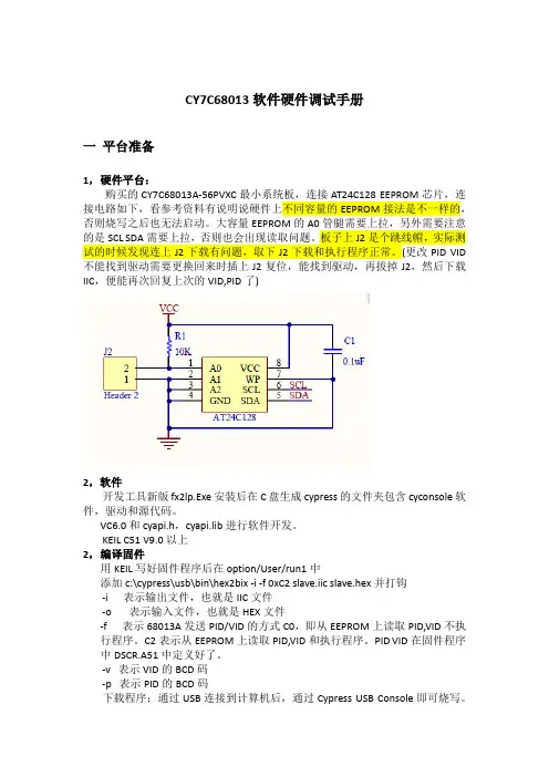
CY7C68013软件硬件调试手册一平台准备1,硬件平台:购买的CY7C68013A-56PVXC最小系统板,连接AT24C128 EEPROM芯片,连接电路如下,看参考资料有说明说硬件上不同容量的EEPROM接法是不一样的,否则烧写之后也无法启动。
大容量EEPROM的A0管腿需要上拉,另外需要注意的是SCL SDA需要上拉,否则也会出现读取问题。
板子上J2是个跳线帽,实际测试的时候发现连上J2下载有问题,取下J2下载和执行程序正常。
(更改PID VID 不能找到驱动需要更换回来时插上J2复位,能找到驱动,再拔掉J2,然后下载IIC,便能再次回复上次的VID,PID了)2,软件开发工具新版fx2lp.Exe安装后在C盘生成cypress的文件夹包含cyconsole软件,驱动和源代码。
VC6.0和cyapi.h,cyapi.lib进行软件开发。
KEIL C51 V9.0以上2,编译固件用KEIL写好固件程序后在option/User/run1中添加c:\cypress\usb\bin\hex2bix -i -f 0xC2 slave.iic slave.hex并打钩-i 表示输出文件,也就是IIC文件-o 表示输入文件,也就是HEX文件-f 表示68013A发送PID/VID的方式C0,即从EEPROM上读取PID,VID不执行程序。
C2表示从EEPROM上读取PID,VID和执行程序。
PID VID在固件程序中DSCR.A51中定义好了。
-v 表示VID的BCD码-p 表示PID的BCD码下载程序:通过USB连接到计算机后,通过Cypress USB Console即可烧写。
打开EZ-USB Interface,点击Lg EEPROM,然后选择刚才生成好的IIC文件可以,下载后重新打开板子电源。
二固件编写我们的固件主要基于官方的例程AN61345,芯片工作于slave-fifo模式,(对于FPGA应该由芯片产生IFCLK,工作于同步模式,对于低速外设应该工作于异步模式(芯片自己产生IFCLK))内部构建2个bulk传输,利用端口2进行out 传输和端口6进行in传输,另外一些参数的设定使用端口0进行控制传输。

用于纳米通道单分子检测的数据采集系统的设计与实现王慧锋;徐英超;颜秉勇【摘要】针对纳米通道单分子检测系统的信号特点和对数据采集的采样精度、采样速率及实时性等要求,设计并实现了基于FPGA和USB2.0接口的数据采集系统;该系统以FPGA作为控制核心,包括数据采集模块、电压输出模块和USB接口电路模块;通过USB2.0接口与计算机连接,实现数据的实时采样和参数的在线配置;此外本系统还采取了低噪声设计;经过相关试验表明,该系统引入的噪声在1 mV内,能够稳定进行数据采集,且采集信号与电压输出信号同步传输,证明该系统能够满足纳米通道单分子检测系统对数据采集的要求.【期刊名称】《计算机测量与控制》【年(卷),期】2015(023)001【总页数】4页(P224-226,230)【关键词】纳米通道单分子检测;数据采集;USB2.0;FPGA;低噪声【作者】王慧锋;徐英超;颜秉勇【作者单位】华东理工大学信息科学与工程学院,上海200237;华东理工大学信息科学与工程学院,上海200237;华东理工大学信息科学与工程学院,上海200237【正文语种】中文【中图分类】TP3030 引言纳米通道单分子检测技术是一种在电极两端电场力驱动下,检测单个分子穿过纳米通道产生离子流信号的方法[1-2]。
分子穿过纳米通道时,会产生一个阻断事件,其阻断事件的变化幅值与其结构相关,通过分析阻断事件的电信号变化能够得到分子的个体行为。
研究人员往往通过计算机来实现对测量数据的分析和针对不同的实验进行设备的控制,因此需要一个“桥梁”来连接计算机与外围的设备,完成数据的转换。
纳米通道单分子检测系统包括检测池、探头、前置放大器、数据采集系统和计算机等几部分。
检测池由电极、电解液和纳米孔组成,通过对电极施加电压信号得到pA 级电流。
探头通过高增益的I-V 转换,实现pA 级电流到mV 级电压的转换。
前置放大器连接探头,对探头的输出信号进行调理放大,并将数据采集系统的输出电压通过探头施加到电极上。
基于CY7C68013的USB2.0数据传输模块设计
1 引言
通用串行总线(USB)[1]是一种电缆总线。
它支持主计算机与许多可同时
访问的外设之间进行数据交换。
使外设的连接具有单一化、即插即用、热插拔
等特点,已经成为个人笔记本电脑和台式机的标准配置接口。
USB 支持3 种传输速率:1.5Mb/s 的低速传输、12Mb/s 的全速传输、480Mb/s 的高速传输。
Cypress 公司的EZ-USB FX2 是一款集成USB2.0 的微处理器,它集成了USB2.0 收发器、SIE(串行接口引擎)、增强的8051 微控制器和可编程的外围接口。
每条指令占四个时钟周期,在48M 晶振下工作时,单指令周期为83.3ns,执行速度远快于标准的8051 单片机。
本文的数据传输模块采用
CY7C68013 高速芯片设计的USB 接口可以实现外部的存储测试电路数据的快速下载,并且上传至计算机保存,显示,处理。
文中重点介绍CY7C68013 的GPIF 接口功能及其在设计中的实现机理。
2 硬件连接设计
2.1 系统连接框图及硬件各部分功能
系统的连接框图如下图1 所示:主要有计算机主机USB 接口,程序存储EEPROM,内置MCU 的USB 接口芯片,电平转换部分组成。
硬件各部分功能:
设备接口:实现模块与测试电路的连接;
电平转换:单片机的输出和工作电压为3.3V 的电压值,而设备的电压
是3.3~5V 之间,电平转换器件实现电压值的匹配;
USB 总线控制器:采用CY7C68013 接口芯片的GPI 接口模式完成控制信号的发送和16bit 宽度数据的读取;。
USB2.0控制器CY7C68013的接口设计实2008-01-20摘要:介绍了一种基于USB2.0控制器CY7C68130的USB-ATA接口,将普通硬盘转化为USB Mass -Storage的解决,文中给出了利用GPIF实现该方案的相关设计方法。
关键词:USB2.0 ATA接口 CY7C68130 GPIF1 引言USB(Universal Serial Bus)接口以其速度快、功耗低、支持即插即用(Plug & Play)、使用安装方便等优点而得到了广泛的应用。
目前USB2.0标准的传输速度已达480Mb/s,这使得USB可以推广到硬盘、信息家电网络产品和其它快速外设。
在某些应用场合,如基于硬盘的大容量数据采集与分析系统中,为了使用方便,需要将普通硬盘转化成海量存储器,这样在使用时就不需关机重启或打开机箱来安装。
本文介绍一种利用带USB接口的单片机芯片CY7C68013来控制普通硬盘的读写,从而半普通硬盘转化为USB2.0海量存储器的.可行方案,本系统可扩展,完全可用于实现基于硬盘的大容量数据采集与分析系统。
2 硬件设计2.1 USB接口芯片本设计选用的是Cypress公司的EZ-USBFX2系列芯片中的CY7C68013,这是一种带USB接口的单片机芯片,虽然采用低价的8051单片机,但仍然能获得很高的速度。
它包括一个8051处理器、一个串行接口引擎(SIE)、一个USB收发器、一个8.5kB片上RAM、一个4 kB FIFO存储器及一个通用可编程接口(GPIF)。
FX2可提供全面集成的解决方案。
它有56SSOP、100TQFP、128TQFP 三种封装,本设计选用占用电路板空间较少的56SSOP封装。
如果要进行扩展,也可选用128TQFP封装。
2.2 ATA接口ATA接口是在ST506的基础上改进而成的,它将控制器集成到驱动器中,采用8个端口寄存器(即命令寄存器)来完成对硬盘的读写,ATA有两种工作模式:PIO模式和DMA模式。
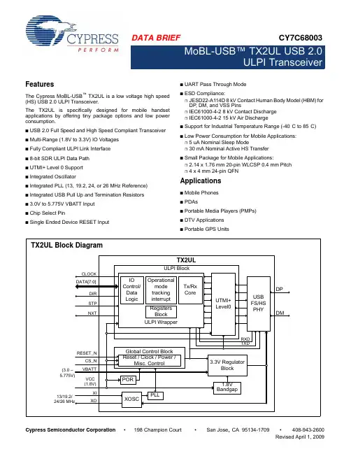
DATA BRIEF CY7C68003MoBL-USB™ TX2UL USB 2.0ULPI TransceiverFeaturesThe Cypress MoBL-USB™ TX2UL is a low voltage high speed (HS) USB 2.0 ULPI Transceiver.The TX2UL is specifically designed for mobile handset applications by offering tiny package options and low power consumption.■USB 2.0 Full Speed and High Speed Compliant Transceiver ■Multi-Range (1.8V to 3.3V) IO Voltages■Fully Compliant ULPI Link Interface■8-bit SDR ULPI Data Path■UTMI+ Level 0 Support■Integrated Oscillator■Integrated PLL (13, 19.2, 24, or 26 MHz Reference)■Integrated USB Pull Up and Termination Resistors■3.0V to 5.775V VBATT Input■Chip Select Pin■Single Ended Device RESET Input ■UART Pass Through Mode■ESD Compliance:❐JESD22-A114D 8 kV Contact Human Body Model (HBM) for DP, DM, and VSS Pins❐IEC61000-4-2 8 kV Contact Discharge❐IEC61000-4-2 15 kV Air Discharge■Support for Industrial Temperature Range (-40°C to 85°C)■Low Power Consumption for Mobile Applications:❐5 uA Nominal Sleep Mode❐30 mA Nominal Active HS Transfer■Small Package for Mobile Applications:❐2.14 x 1.76 mm 20-pin WLCSP 0.4 mm Pitch❐4 x 4 mm 24-pin QFNApplications■Mobile Phones■PDAs■Portable Media Players (PMPs)■DTV Applications■Portable GPS UnitsFunctional OverviewUTMI+ Low Pin Interface (ULPI)This block conforms to the ULPI Specification. It supports the 8-bit wide SDR data path. The primary IOs of this block support multi-range LVCMOS signaling from 1.8V to 3.3V (±5%). The level used is automatically selected by the voltage applied to Vccio and is set at any voltage between 1.8V and 3.3V. Oscillator (OSC)This block meets the requirements of both the on-chip PLL and the USB-IF requirements for clock parameters. It is a fundamental mode parallel resonant oscillator with a maximum ESR of 60 ohms. It supports the following:■Integrated Crystal Oscillator - 13, 19.2, 24, or 26 MHz crystal ■13, 19.2, 24, or 26 MHz LVCMOS single ended input clock on XI Phase Locked Loop (PLL)The PLL meets all clock stability requirements imposed by this device and the USB standard. It supports all requirements to make the device compliant to the USB 2.0 specifications. It also has a fractional multiplier that enables it to supply the correct frequency to the device when it is presented with a 13, 19.2, 24, or 26 MHz reference clock.Power On Reset (POR)This block provides a power on reset signal (internal) based on the input supply. An internal power on reset is generated when VCC input rises above VPOR(trip).Reset (RESET_N)The three major functions of RESET_N pin are as follows:■Reset TX2UL■Place TX2UL into Sleep Mode■Place TX2UL into Configuration ModeWhen the RESET_N pin is asserted (low) for tSTATE (tSTATE is specified in Table 21 on page 19), the TX2UL enters into either Sleep Mode or Configuration Mode depending on the CS_N state. When RESET_N is asserted while CS_N is asserted, TX2UL enters into Sleep Mode. When RESET_N is asserted for tSTATE while CS_N is deasserted, TX2UL enters into Configu-ration Mode. In these modes, all the pins in the ULPI interface are tri-stated. If the RESET_N pin is not used, it must be pulled high. For more information about different modes of configu-ration, see Table 5 on page 4.DP and DM pinsThe DP and DM pins are the differential pins for the USB. They must be connected to the corresponding DP and DM pins of the USB receptacle.Chip Select (CS_N)This signal pin is available only in 24-pin QFN package. The two major functions of CS_N are as follows:■Tri-state the ULPI bus output pins■Associate with RESET_N to place TX2UL in the Sleep mode When the CS_N pin is deasserted (high), all the pins in the ULPI interface are tri-stated.USB2 Transceiver Macrocell Interface (UTMI+)This block conforms to the UTMI+ Level 0 standard. It performs all the UTMI to USB translation.Global ControlThis block is the digital control logic that ties the blocks of the device together. Functions performed include pull up control, over current protect control, and more.Full Speed and High Speed USB Transceivers (FS/HS) The FS and HS Transceivers comply fully with the USB 2.0 specifications.USB Pull up and Intr Detect, Termination Resistors (Pull up / TERM)These blocks contain the USB pull up and termination resistors as specified by the USB 2.0 specification.UART Pass Through ModeTX2UL supports Carkit UART Pass Through Mode. When the Carkit Mode bit in the Interface Control register is set, it enables the Link to communicate through the DP/DM to a remote system using UART signaling. By default, the clock is powered down when the TX2UL enters Carkit Mode. Entering and exiting the Carkit Mode is identical to the Serial Mode. Table1, Table2, and Figure1 show the UART Signal Mapping between the DP/DM and DATA[1:0] at ULPI interface.Figure 1. UART Signal Mapping in Pass Through Mode Table 1. UART Signal Mapping at ULPI Interface Signal Maps to Direction Descriptiontxd DATA[0]IN UART TXD signalrouted to DM pin rxd DATA[1]OUT UART RXD signalrouted to DP pin Reserved DATA[7:2]-ReservedTable 2. UART Signal Mapping at USB Interface SignalMaps to Direction Description TXD DM OUT UART TXD signalRXD DP INT UART RXD signalClockingTX2UL supports external crystal and clock inputs at the 13, 19.2, 24, and 26 MHz frequencies. The internal PLL applies the proper clock multiply option depending on the input frequency. For appli-cations that use an external clock source to drive XI, the XO pin (in 24-pin QFN package) is left floating. TX2UL has an on-chip oscillator circuit that uses an external 13, 19.2, 24, or 26 MHz (±100 ppm) crystal with the following characteristics:■Parallel Resonant■Fundamental Mode■750 mW Drive Level■12 pF (5 percent tolerance) Load Capacitors■150 ppmTX2UL operates on one of two primary clock sources:■LVCMOS square wave clock input driven on the XI pin■Crystal generated sine wave clock on the XI and XO pins The selection between input clock source and frequency on the XI pin is determined by the Chip Configuration register loaded through the RESET_N during Configuration Mode. The external clock source requirements are shown in Figure 3 on page 4. Figure 2. Crystal ConfigurationPower DomainsThe TX2UL has three power supply domains:■VCC■VIO■VBATTTX2UL has two grounds:■VSS■VSSBATTVCCThis is the core 1.8V power supply for the TX2UL. It can range anywhere from 1.7V to 1.9V during actual operation.VIOThis is the 1.8V to 3.3V multi range supply to the I/O ring. It can range anywhere from 1.7V to 3.6V during actual operation.VBATTThis is the battery input supply that powers the 3.3V Regulator block. It can range anywhere from 3.0 to 5.775V during actual operation.Voltage RegulatorThe internal 3.3V regulator block regulates the VBATT supply to the internal 3.3V supply for the USBIO and XOSC blocks. If the supply voltage at VBATT is below 3.3V, the regulator block switches the VBATT supply directly for the USBIO and XOSC blocks.Power Supply SequenceTX2UL does not require power supply sequence. All power supplies are independently sequenced without damaging the part. All supplies are up and stable for the device to function properly. The analog block contains circuitry that senses the power supply to determine when all supplies are valid.Table 3. External Clock RequirementsParameter DescriptionSpecificationUnit Min MaxVn Supply Voltage Noise at frequencies < 50 MHz20mV p-p PN_100Input Phase Noise at 100 Hz–75dBc/Hz PN_1k Input Phase Noise at 1 kHz offset–104dBc/Hz PN_10k Input Phase Noise at 10 kHz offset–120dBc/Hz PN_100k Input Phase Noise at 100 kHz offset–128dBc/Hz PN_1M Input Phase Noise at 1 MHz offset–130dBc/Hz Duty Cycle3070%Maximum Frequency Deviation150ppmOperation ModesThere are six operation modes available in TX2UL. They are:■Normal Operation Mode■Configuration Mode■ULPI Low Power Mode■Sleep Mode■Carkit UART Pass Through Mode■Tri-state ULPI Interface Output Mode (only available in 24-pin QFN package)When changing the operation modes, if the current and changing modes are not the Normal Operation Mode, TX2UL first changes to the Normal Operation Mode. For example, to change from ULPI Low power mode to Sleep mode, TX2UL changes to Normal operation mode first, and then changes to Sleep mode. The Mode Change State diagram in Figure3 shows the mode change path of TX2UL. The entries of the six operations modes (20-pin CSP package has 5 operation modes) are listed in Table4 and Table5. There are three mode change transactions that require the RESET_N assert or deassert with tSTATE (see Table 21 on page 19 for tSTATE). These three mode change transactions are:■Change from Normal Operation Mode to Configuration Mode – RESET_N is required to assert with tSTATE■Change from Configuration Mode to Normal Operation Mode – RESET_N is required to de-assert with tSTATE■Change from Normal Operation Mode to Sleep Mode – RESET_N is required to assert with tSTATEFigure 3.Mode Change State DiagramTable 4. TX2UL 20-Pin CPS Package Operation ModesRESET_N Mode0 (Low)Sleep Mode1 (High)Normal Operation Mode1 (High)Enter into ULPI Low Power Mode by setting Sus-pendM register bit (in Function Control Register) to0 during the Normal Operation Mode.1 (High)Enter into Carkit UART Pass Through Mode by set-ting Carkit Mode register bit (in Interface ControlRegister) to 1 during the Normal Operation Mode.0 (Low) when Power On (VCC On)Enter into Configuration ModeTable 5. TX2UL 24-Pin QFN Package Operation ModesCS_N RESET_N Mode0 (Low)0 (Low)Sleep Mode0 (Low) 1 (High)Normal Operation Mode0 (Low) 1 (High)Enter into ULPI Low Power Modeby setting SuspendM register bit (inFunction Control Register) to 0 dur-ing the Normal Operation Mode.0 (Low) 1 (High)Enter into Carkit UART PassThrough Mode by setting CarkitMode register bit (in Interface Con-trol Register) to 1 during the Nor-mal Operation Mode.1 (High)0 (Low)Configuration Mode1 (High) 1 (High)Tri-state ULPI Interface output pinsRevised April 1, 2009Page 5 of 5All products and company names mentioned in this document may be the trademarks of their respective holders.© Cypress Semiconductor Corporation, 2007-2009. The information contained herein is subject to change without notice. Cypress Semiconductor Corporation assumes no responsibility for the use of any circuitry other than circuitry embodied in a Cypress product. Nor does it convey or imply any license under patent or other rights. Cypress products are not warranted nor intended to be used for medical, life support, life saving, critical control or safety applications, unless pursuant to an express written agreement with Cypress. Furthermore, Cypress does not authorize its products for use as critical components in life-support systems where a malfunction or failure may reasonably be expected to result in significant injury to the user. The inclusion of Cypress products in life-support systems application implies that the manufacturer assumes all risk of such use and in doing so indemnifies Cypress against all charges.Any Source Code (software and/or firmware) is owned by Cypress Semiconductor Corporation (Cypress) and is protected by and subject to worldwide patent protection (United States and foreign),United States copyright laws and international treaty provisions. Cypress hereby grants to licensee a personal, non-exclusive, non-transferable license to copy, use, modify, create derivative works of,and compile the Cypress Source Code and derivative works for the sole purpose of creating custom software and or firmware in support of licensee product to be used only in conjunction with a Cypress integrated circuit as specified in the applicable agreement. Any reproduction, modification, translation, compilation, or representation of this Source Code except as specified above is prohibited without the express written permission of Cypress.Disclaimer: CYPRESS MAKES NO WARRANTY OF ANY KIND, EXPRESS OR IMPLIED, WITH REGARD TO THIS MATERIAL, INCLUDING, BUT NOT LIMITED TO, THE IMPLIED WARRANTIES OF MERCHANTABILITY AND FITNESS FOR A PARTICULAR PURPOSE. Cypress reserves the right to make changes without further notice to the materials described herein. Cypress does not assume any liability arising out of the application or use of any product or circuit described herein. Cypress does not authorize its products for use as critical components in life-support systems where a malfunction or failure may reasonably be expected to result in significant injury to the user. The inclusion of Cypress’ product in a life-support systems application implies that the manufacturer assumes all risk of such use and in doing so indemnifies Cypress against all charges. Use may be limited by and subject to the applicable Cypress software license agreement.The operation and configuration modes are described in Operation Modes on page 4 and Configuration Mode on page 14respectively. The ULPI Low power mode and Sleep mode are described in the following sections:ULPI Low Power ModeIn this mode, the link optionally places the TX2UL in low power mode when the USB is suspended. TX2UL powers down all the circuitry except for the interface pins and full speed receiver. To enter low power mode, the link must set SuspendM in the Function Control register to 0b. The TX2UL clock is stopped for a minimum of five cycles after TX2UL accepts the register write.To exit the low power mode, the link signals TX2UL to exit the mode by asynchronously asserting a signal, STP . The TX2UL wakes up its internal circuitry and when it meets the ULPI timing requirements it deasserts DIR. The SuspendM register is set to 1b.Sleep ModeSleep mode is entered by asserting RESET_N during the Normal Operation Mode. When RESET_N is driven low for tSTATE (see Table 21 on page 19 for tSTATE requirement) while CS_N is low,TX2UL enters into Sleep Mode. VCC must remain supplied (ON)during the sleep mode. This mode powers down all internal circuitry except the RESET_N pin and the chip_config register.The ULPI interface bus is tri-stated. During the Sleep Mode ensure that:■The ULPI interface IOs is either floating or driven high by the link ■DP and DM are either floating or pull to 0V ■Deassert RESET_N to exit the Sleep Mode.VID and PIDThe VID and PID are hard coded into Product ID and Vendor ID registers (read only) as shown in Table 6.Table 6. Immediate Register Values for VID and PIDField NameSize (bit)Address (6 bits)Value Rd Wr Set Clr Vendor ID (VID) Low 800h ---B4h Vendor ID (VID) High 801h ---04h Product ID (PID) Low 802h ---03h Product ID (PID) High803h---68h。
CY7C68013芯片的USB接口固件设计来源:单片机及嵌入式系统应用作者:北京交通大学李强伍坚姚冬苹USB接口(Universal Serial Bus)是一种通用的高速串行接口。
它最主要的特点是高速传输特性,可以很好地解决海量数据在嵌入式系统与PC机之间的互传问题;同时USB接口还具有热插拔、速度快(具有3种数据传输模式,即低速、全速、高速;最快可达480 Mbp s)和扩展性好(最多可以连接127个USB设备)等特点,从而使得USB接口得到了广泛的应用。
1 USB芯片CY7C68013介绍CY7C68013属于Cypress公司的FX2系列产品,是Cypress公司生产的第一款USB2.0芯片。
CYTC68013是一个带增强型MCS51内核和USB接口的单片机,完全遵从USB2.O 协议,可提供高达480 Mbps的传输率;内部集成PLL(锁相环),最高可使5l内核工作在4 8MHz;对外提供两个串口,可以方便地与外部通信;片内拥有8 KB的RAM,可完全满足系统每次传输数据的需要,无需再外接RAM。
由于芯片内部没有ROM,一旦USB设备断开与PC的连接,程序代码将无法保存,需要每次在PC机接入USB设备后,重新下载。
另外,CY7C68013支持一种“E2PROM引导方式”,即先将固件下载到片外E2PROM中,当每次USB设备通电后,FX2自动将片外E2PROM中的程序读入芯片中。
CY7C68013与外设有主/从两种接口方式:可编程接口GPIF和Slave FIFO。
可编程接口GPIF是主机方式,可以通过软件编写读/写控制时序,灵活方便,几乎可以与所有8/16位接口的控制器、存储器和总线实现无缝连接。
Slave FTFO是从机方式,外部控制器可以像对待普通FIFO一样对芯片内的多个缓冲区进行读/写;S1ave FIFO方式也可以灵活配置,以适应不同的需要。
2 硬件设计思想USB数据传输流程如图l所示。
Distributed by:✦ 1-800-831-4242The content and copyrights of the attachedmaterial are the property of its owner.Features•Automatic power-down when deselected •CMOS for optimum speed/power •High speed —15 ns•Low active power—660 mW (commercial)—688 mW (military—20 ns)•Low standby power —110 mW (20 ns)•TTL-compatible inputs and outputs•Capable of withstanding greater than 2001V electro-static discharge •V IH of 2.2VFunctional DescriptionThe CY7C128A is a high-performance CMOS static RAM or-ganized as 2048 words by 8 bits. Easy memory expansion isprovided by an active LOW Chip Enable (CE), and active LOW Output Enable (OE) and three-state drivers. The CY7C128A has an automatic power-down feature, reducing the power consumption by 83% when deselected.Writing to the device is accomplished when the Chip Enable (CE) and Write Enable (WE) inputs are both LOW.Data on the eight I/O pins (I/O 0 through I/O 7) is written into the memory location specified on the address pins (A 0 through A 10).Reading the device is accomplished by taking Chip Enable (CE) and Output Enable (OE) LOW while Write Enable (WE)remains HIGH. Under these conditions, the contents of the memory location specified on the address pins will appear on the eight I/O pins.The I/O pins remain in high-impedance state when Chip En-able (CE) or Output Enable (OE) is HIGH or Write Enable (WE)is LOW.The CY7C128A utilizes a die coat to insure alpha immunity.Logic Block Diagram Pin ConfigurationsC128A –1A 1A 2A 4A 5A 6COLUMN DECODERR O W D E C O D E RS E N S E A M P SINPUT BUFFERPOWER DOWNWE OEI/O 0CE I/O 1I/O 2I/O 3Top ViewLCC 12345678910111415162019181721242322Top ViewDIP/SOJ/SOIC 1213A 6A 5A 4A 3WE V CCA 8A 9A 10I/O 5I/O 4I/O 3C128A –2A 7I/O 0I/O 1CE OE 128x 16x 8ARRAYI/O 7I/O 6I/O 5I/O 47C128AA 0C128A –3A 3A 7A 8A 9A 1024456789103212311 12 13 14 1522212019181716A 5V C C 7C128A A 62I /O A 4A 3A 2A 1WE CE A 0A 9I/O 2GNDI/O 7I/O 6A 2A 1A 03I /O 4I /O 5I /O G N D A 7A 8OE A 10I/O 7I/O 6I/O 0I/O 1Selection Guide7C128A-157C128A-207C128A-257C128A-357C128A-45Maximum Access Time (ns)1520253545Maximum Operating Current (mA)Commercial 120120*********Military -125125125125Maximum Standby Current (mA)Commercial 40 20202020Military-20202020Jameco Part Number 242683Maximum Ratings(Above which the useful life may be impaired. For user guide-lines, not tested.)Storage Temperature .................................–65°C to +150°C Ambient Temperature withPower Applied.............................................–55°C to +125°C Supply Voltage to Ground Potential(Pin 28 to Pin 14)...........................................–0.5V to +7.0V DC Voltage Applied to Outputsin High Z State...............................................–0.5V to +7.0V DC Input Voltage............................................–3.0V to +7.0V Output Current into Outputs (LOW).............................20 mA Static Discharge Voltage.......................................... >2001V (per MIL-STD-883, Method 3015)Latch-Up Current.................................................... >200 mA Operating RangeRangeAmbientTemperature V CC Commercial0°C to +70°C 5V ± 10% Military[1]–55°C to +125°C 5V ± 10%Electrical Characteristics Over the Operating Range[2]7C128A-157C128A-207C128A-257C128A-35,45 Parameter Description Test Conditions Min.Max.Min.Max.Min.Max.Min.Max.UnitV OH Output HIGHVoltage V CC = Min.,I OH = –4.0 mA2.4 2.4 2.4 2.4VV OL Output LOWVoltageV CC = Min., I OL = 8.0 mA0.40.40.40.4VV IH Input HIGHVoltage2.2V CC 2.2V CC 2.2V CC 2.2V CC VV IL Input LOWVoltage[3]–0.50.8–0.50.8–0.50.8–0.50.8VI IX Input LoadCurrentGND < V I < V CC–10+10–10+10–10+10–10+10µAI OZ Output LeakageCurrent GND < V I < V CCOutput Disabled–10+10–10+10–10+10–10+10µAI OS Output ShortCircuitCurrent[4]V CC = Max.,V OUT = GND–300–300–300–300mAI CC V CC OperatingSupply Current V CC = Max.I OUT = 0 mACom’l120120120120mAMil-125125125I SB1Automatic CEPower-DownCurrent Max. V CC,CE > V IH,Min. Duty Cycle= 100%Com’l40402020mAMil-404020I SB2Automatic CEPower-DownCurrent Max. V CC,CE1 >V CC–0.3V,V IN > V CC–0.3Vor V IN < 0.3VCom’l40202020mAMil-202020Capacitance[5]Parameter Description Test Conditions Max.UnitC IN Input Capacitance T A = 25°C, f = 1 MHz,V CC = 5.0V10pFC OUT Output Capacitance10pF Notes:1.T A is the “instant on” case temperature.2.See the last page of this specification for Group A subgroup testing information.3.V IL (min.) = –3.0V for pulse durations less than 30 ns.4.Not more than 1 output should be shorted at one time. Duration of the short circuit should not exceed 30 seconds.5.Tested initially and after any design or process changes that may affect these parameters.AC Test Loads and Waveforms3.0V 5V OUTPUTR1 481ΩR2255Ω30pF INCLUDING JIG AND SCOPE GND90%10%90%10%≤5ns ≤5ns5V OUTPUTC128A –4R1 481ΩR2255Ω5pFINCLUDING JIG AND SCOPEC128A –5(a)(b)OUTPUT1.73VEquivalent to:TH É V ENIN EQUIVALENTALL INPUT PULSES 167ΩSwitching Characteristics Over the Operating Range [2, 6]7C128A-157C128A-207C128A-257C128A-357C128A-45Parameter DescriptionMin.Max.Min.Max.Min.Max.Min.Max.Min.Max.UnitREAD CYCLE t RC Read Cycle Time 1520253545ns t AA Address to Data Valid1520253545ns t OHA Data Hold from Address Change 55555ns t ACE CE LOW to Data Valid 1520253545ns t DOE OE LOW to Data Valid 1010121520ns t LZOE OE LOW to Low Z 33333ns t HZOE OE HIGH to High Z [7]88101215ns t LZCE CE LOW to Low Z [8]55555ns t HZCE CE HIGH to High Z [7, 8]88101515ns t PU CE LOW to Power-Up 0ns t PD CE HIGH to Power-Down 1520202025ns WRITE CYCLE [9]t WC Write Cycle Time1520202540ns t SCE CELOW to Write End 1215202530ns t AW Address Set-Up to Write End 1215202530ns t HA Address Hold from Write End 00000ns t SA Address Set-Up to Write Start 00000ns t PWE WEPulse Width 1215152020ns t SD Data Set-Up to Write End1010101515ns t HD Data Hold from Write End 0ns t HZWE WE LOW to High Z [7]7771015ns t LZWEWE HIGH to Low Z55555nsNotes:6.Test conditions assume signal transition time of 5 ns or less, timing reference levels of 1.5V, input pulse levels of 0 to 3.0V, and output loading of the specifiedI OL /I OH and 30-pF load capacitance.7.t HZOE , t HZCE , and t HZWE are specified with C L = 5 pF as in part (b) of AC T est Loads. Transition is measured ±500 mV from steady state voltage.8.At any given temperature and voltage condition, t HZCE is less than t LZCE for any given device.9.The internal write time of the memory is defined by the overlap of CE LOW and WE LOW. Both signals must be LOW to initiate a write and either signal can terminatea write by going HIGH. The data input set-up and hold timing should be referenced to the rising edge of the signal that terminates the write.Switching WaveformsRead Cycle No. 1[10, 11]Read Cycle No. 2[10, 12]Write Cycle No. 1 (WE Controlled)[9, ]Notes:10.WE is HIGH for read cycle.11.Device is continuously selected. OE, CE = V IL .12.Address valid prior to or coincident with CE transition LOW.13.Data I/O pins enter high-impedance state, as shown, when OE is held LOW during write.ADDRESSC128A –6DATA OUTPREVIOUS DATA VALIDDATA VALIDt RCt AAt OHA50%50%DATA VALIDt RCt ACEt DOEt LZOEt LZCEt PUDATA OUTHIGH IMPEDANCEIMPEDANCEI CC I SBt HZOE t HZCEt PDOECEHIGH C128A –7V CC SUPPLY CURRENTt WCDATA UNDEFINEDHIGH IMPEDANCEt SCEt AWt SAt PWEt HAt HDt HZWEt LZWEt SDC128A –8CEWEDATA INDATA I/OADDRESSDATA IN VALIDWrite Cycle No. 2 (CE Controlled)[9, 13, 14]Notes:14.If CE goes HIGH simultaneously with WE HIGH, the output remains in a high-impedance state.Switching Waveforms (continued)t WCDATA UNDEFINEDHIGH IMPEDANCEt SCEt AWt SAt PWEt HAt HDt HZWEt SDADDRESSCEWEDATA INDATA I/OC128A –9DATA IN VALID Typical DC and AC Characteristics1.21.41.00.60.40.24.04.55.05.56.01.61.41.21.00.8–5525125–55251251.21.00.8N O R M A L I Z E D t A A120100806040200.01.02.03.04.0O U T P U T S O U R C E C U R R E N T (m A )SUPPLY VOLTAGE(V)NORMALIZED SUPPLY CURRENT vs.SUPPLY VOLTAGENORMALIZED ACCESS TIME vs.AMBIENT TEMPERATURE AMBIENT TEMPERATURE(°C)NORMALIZED SUPPLY CURRENT vs.AMBIENT TEMPERATURE AMBIENT TEMPERATURE(°C)OUTPUT VOLTAGE(V)OUTPUT SOURCE CURRENT vs.OUTPUT VOLTAGE 0.00.8N O R M A L I Z E D t A ASUPPLY VOLTAGE(V)NORMALIZED ACCESS TIME vs.SUPPLY VOLTAGE 120140*********0.01.02.03.04.0O U T P U T S I N K C U R R E N T (m A )080OUTPUT VOLTAGE(V)OUTPUT SINK CURRENT vs.OUTPUT VOLTAGE0.60.40.20.0N O R M A L I Z E D I C C , I S BN O R M A L I Z E D I C C , I S BI SBV CC = 5.0V V IN = 5.0VI CCI CCV CC = 5.0VV CC =5.0V T A = 25°CV CC =5.0V T A = 2 5°C)I SB0.60Typical DC and AC Characteristics (continued)3.02.52.01.51.00.50.01.02.03.04.0N O R M A L I Z E D I P OSUPPLY VOLTAGE(V)TYPICAL POWER-ON CURRENT vs.SUPPLY VOLTAGE 30.025.020.015.010.05.00200400600800D E L T A t (n s )A ACAPACITANCE (pF)TYPICAL ACCESS TIME CHANGE vs.OUTPUT LOADING1.41.21.010203040N O R M A L I Z E D I C CCYCLE FREQUENCY (MHz)NORMALIZED I CC vs.CYCLE TIME0.05.00.010000.8V CC = 4.5V T A = 25°CV CC = 5.0V T A = 25°C V IN = 0.5V 0.91.11.3Ordering InformationSpeed (ns)Ordering Code Package Name Package TypeOperating Range 15CY7C128A-15PC P1324-Lead (300-Mil) Molded DIP CommercialCY7C128A-15VC V1324-Lead Molded SOJCY7C128A-15SC S1324-Lead (300-Mil) Molded SOIC 20CY7C128A-20PC P1324-Lead (300-Mil) Molded DIP CommercialCY7C128A-20VC V1324-Lead Molded SOJCY7C128A-20SC S1324-Lead (300-Mil) Molded SOIC CY7C128A-20DMB D1424-Lead (300-Mil) CerDIPMilitary CY7C128A-20LMB L5324-Pin Rectangular Leadless Chip Carrier 25CY7C128A-25PC P1324-Lead (300-Mil) Molded DIP CommercialCY7C128A-25VC V1324-Lead Molded SOJCY7C128A-25SC S1324-Lead (300-Mil) Molded SOIC CY7C128A-25DMB D1424-Lead (300-Mil) CerDIP Military35CY7C128A-35PC P1324-Lead (300-Mil) Molded DIP CommercialCY7C128A-35VC V1324-Lead Molded SOJCY7C128A-35SC S1324-Lead (300-Mil) Molded SOIC CY7C128A-35DMB D1424-Lead (300-Mil) CerDIP Military45CY7C128A-45PC P1324-Lead (300-Mil) Molded DIP CommercialCY7C128A-45VC V1324-Lead Molded SOJCY7C128A-45SC S1324-Lead (300-Mil) Molded SOIC CY7C128A-45DMB D1424-Lead (300-Mil) CerDIPMilitaryCY7C128A-45LMBL5324-Pin Rectangular Leadless Chip CarrierMILITARY SPECIFICATIONS Group A Subgroup Testing DC CharacteristicsParameter SubgroupsV OH1, 2, 3V OL1, 2, 3V IH1, 2, 3V IL Max.1, 2, 3I IX1, 2, 3I OZ1, 2, 3I CC1, 2, 3I SB1, 2, 3 Switching Characteristics Parameter Subgroups READ CYCLEt RC7, 8, 9, 10, 11 t AA7, 8, 9, 10, 11 t OHA7, 8, 9, 10, 11 t ACE7, 8, 9, 10, 11 t DOE7, 8, 9, 10, 11 WRITE CYCLEt WC7, 8, 9, 10, 11 t SCE7, 8, 9, 10, 11 t AW7, 8, 9, 10, 11 t HA7, 8, 9, 10, 11 t SA7, 8, 9, 10, 11 t PWE7, 8, 9, 10, 11 t SD7, 8, 9, 10, 11t HD7, 8, 9, 10, 11Package Diagrams24-Lead(300-Mil)CerDIP D14MIL-STD-1835D-9Config.A51-8003124-Pin Rectangular Leadless Chip Carrier L5351-80066Package Diagrams (continued)24-Lead(300-Mil)Molded DIP P13/P13A51-85013-A24-Lead(300-Mil)Molded SOJ V1351-85030-ACY7C128A Document #: 38-05028 Rev. **Page 10 of 10Document Title: CY7C128A 2K x 8 Static RAM Document Number: 38-05028REV.ECN NO.Issue Date Orig. of Change Description of Change**10681409/10/01SZV Change from Spec number: 38-00094 to 38-05028。
基于CY7C68013A芯片的USB键盘的设计陈喜春【摘要】Because the characteristics of high transmission speed, small package, and the ability of power supply, the USB inter- face has been widely used in computer peripheral equipment. In this paper, the principle of IC CYTC68013A made by Cypress is discussed, and also it discusses how to design an USB keyboard using CY7C68013A.%由于具备传输速率高、体积小等特点,USB接口广泛地应用于计算机外部硬件设计。
针对此介绍了Cypress 公司的CYTC68013A芯片的基本原理,以及使用CY7C68013A芯片进行USB键盘设计的方法。
【期刊名称】《山西电子技术》【年(卷),期】2012(000)001【总页数】3页(P6-7,12)【关键词】USB;CY7C68013A;键盘【作者】陈喜春【作者单位】石家庄机械化步兵学院军事模拟训练中心,河北石家庄050083【正文语种】中文【中图分类】TP319USB接口具有传输速率高,体积小,可向外供电等特点,因此使得计算机与外部硬件设备之间的连接和使用都十分方便。
目前,计算机的外围设备中,例如鼠标、键盘、打印机都开始采用USB接口实现。
本文中,将介绍Cypress公司的USB接口芯片——CY7C68013A,并介绍基于 CY7C68013A实现的USB键盘。
1 CY7C68013A芯片简介一个典型的USB应用系统由USB设备、USB主机和USB电缆组成,USB主机一般指具有USB接口的计算机,连接到主机USB端口的外部设备一般称为USB设备。
关于CY7C68013A在Keil中代码及数据地址配置的问题
⽬前USB开发中常⽤的芯⽚是CYPRESS公司的CY7C68013A,注意带A的版本和不带A的版本差别相当⼤,68013A不但将RAM的容量扩充为16KB(不带A的版本只有8KB),同时功耗极⼤地降低。
我在使⽤68013时不但芯⽚发热量⾮常⼤,时间长了就出现不稳定。
⼤家开发是⼀般从CYPRESS提供的开发包(CySuiteUSB_3_4_7_B204.exe)的例程开始,⽽例程中给出的⼀般都是很简单的例⼦,代码量和数据量都相对很⼩。
如果只是应⽤于简单的产品没有什么问题,但⼀旦代码量增⼤时问题便出现了,我刚开始的感觉是只要代码量超过4K程序便飞了。
本来以为买到了假货,后来分析才发现是keil配置的问题。
在⽰例⼯程中,code memory和和Xdata memory 的size给的都很⼩,⽆法使⽤68013A提供的全部ram空间,可按照下图进⾏配置⼀般就⾜够使⽤了,可更具数据量和代码量适量进⾏调整,如数据量⽐较⼤的时候可增⼤Xdatamemory的size,注意code和data之和不要超过16K。
前0x80的地址68013A预留了,所以开始地址为0x80。
另⼀个注意的是BL51Locate选项卡中把Use Memory Layout from Target Dialog选项打勾。
Ports模式下CY7C68013和FPGA的数据通信,Ports模式,通信协议,CY7C68013,FPGA引言通用串行总线(USB)具有快速、双向、大批量传输、廉价以及可实现热插拔等优点,Cypress公司的FX2系列芯片之一CY7C68013是最早符合USB2.0标准的微控制器,集成了符合USB2.0的收发器、串行接口引擎(SIE)、增强型8051内核以及可编程的外围接口,实现基于USB2.0的接口数据通信,CY7C68013可配置成3种不同的接口模式;Ports(端口模式)、GPIFMaster (可编程接口模式)和SlaveFIFO(主从模式),其中,后两种模式利用其内部集成引言通用串行总线(USB)具有快速、双向、大批量传输、廉价以及可实现热插拔等优点,Cypress公司的FX2系列芯片之一CY7C68013是最早符合USB2.0标准的微控制器,集成了符合USB2.0的收发器、串行接口引擎(SIE)、增强型8051内核以及可编程的外围接口,实现基于USB2.0的接口数据通信,CY7C68013可配置成3种不同的接口模式;Ports(端口模式)、GPIFMaster(可编程接口模式)和Slave FIFO(主从模式),其中,后两种模式利用其内部集成的可以独立于微处理器而自动处理USB事务的硬件(USB核),数据的传输通过执行USB本身的协议来完成,微处理器可不参与数据传输,从而使数据的传输速率大大地提高,同时也简化了固件代码的编写。
后两种方式由于克服了微处理器这个带宽"瓶颈",因而广泛应用于大批量的数据传输,如图像、视频等信号的采集。
而对前一种Ports(端口模式),文献中介绍较少,作为一种最基本的数据传输方式,其数据传输主要由固件程序完成,需要CPU的参与,因此数据传输速率比较低,适用于传输速率要求不高的场合,而且由于FX2内部集成有8051内核,对一个刚从单片机的开发过渡到USB开发的工程人员来说,也不失是一种有效的数据传输方式,现以一个工程开发的实例来详细说明一下在Ports模式下如何实现数据一双向传输。