
A1391, A1392, A1393, and A1395
Micro Power 3 V Linear Hall Effect Sensors with Tri-State Output and User Selectable Sleep Mode
A1391, A1392, A1393, and A1395
Terminal List Table
Pin Name Function
1VCC Supply 2OUT Output 3GND Ground 4GND Ground
5 ˉS ˉ ˉL ˉ ˉE ˉ ˉE ˉ ˉP ˉ Toggle sleep mode
6
VREF
Supply for ratiometric reference
Despite the low power consumption of the circuitry in the A139x, the features required to produce a highly-accurate linear Hall effect IC have not been compromised. Each BiCMOS monolithic circuit integrates a Hall element, improved temperature-compensating circuitry to reduce the intrinsic sensitivity drift of the Hall element, a small-signal high-gain amplifier, and proprietary dynamic offset cancellation circuits. End of line, post-packaging, factory programming allows precise control of device sensitivity and offset.
These devices are available in a small 2.0 × 3.0 mm, 0.75 mm nominal height microleaded package (MLP/DFN). It is Pb (lead) free, with 100% matte tin leadframe plating.
Absolute Maximum Ratings*
Supply Voltage
V CC 8V Reverse-Supply Voltage
V RCC –0.1V Ratiometric Supply Reference Voltage
V REF 7V Reverse-Ratiometric Supply Reference Voltage V RREF –0.1V Logic Supply Voltage
V ˉS ˉ ˉL ˉ ˉE ˉ ˉE ˉ ˉP ˉ (V CC > 2.5 V)
32V Reverse-Logic Supply Voltage V RˉS ˉ ˉL ˉ ˉE ˉ ˉE ˉ ˉP ˉ –0.1V Output Voltage
V OUT V CC + 0.1V Reverse-Output Voltage V ROUT –0.1V Operating A mbient Temperature T A Range S –20 to 85oC Junction Temperature T J (MAX)165oC StorageTemperature
T stg
–65 to 170
oC
*All ratings with reference to ground
Selection Guide
Part Number Sensitivity
(mV / G, Typ.)
Packing
A1391SEHLT-T 1.25
7-in. reel, 3000 pieces/reel A1392SEHLT-T 2.50
7-in. reel, 3000 pieces/reel A1393SEHLT-T 5
7-in. reel, 3000 pieces/reel A1395SEHLT-T
10
7-in. reel, 3000 pieces/reel
VCC OUT GND
VREF GND
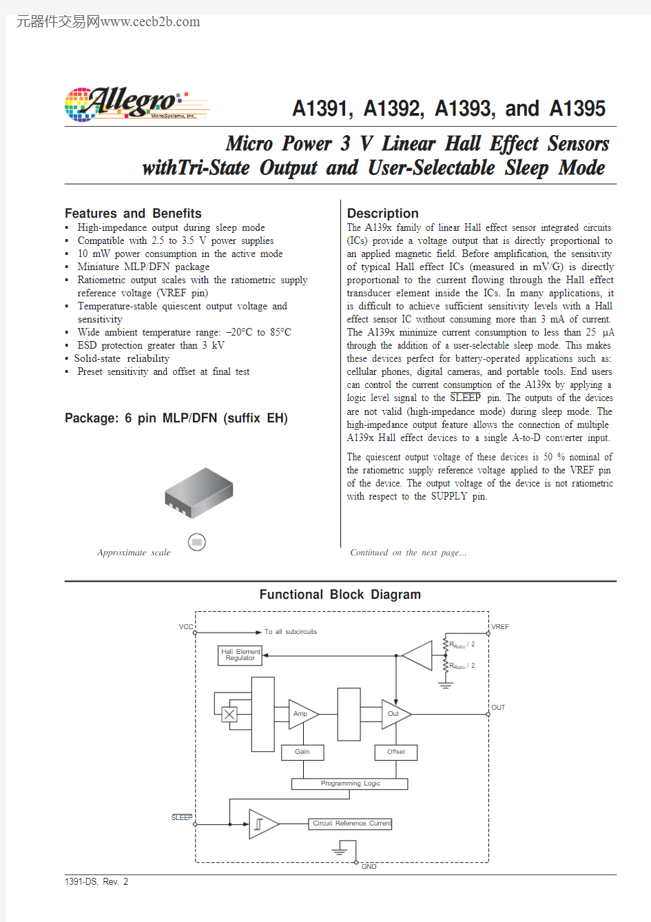
SLEEP Description (continued)
Pin-out Diagram
Micro Power 3 V Linear Hall Effect Sensors with Tri-State Output and User Selectable Sleep Mode
A1391, A1392, A1393, and A1395
Device Characteristics Tables
ELECTRICAL CHARACTERISTICS valid through full operating ambient temperature range, unless otherwise noted
Characteristic
Symbol
Test Conditions
Min.Typ.1Max.Units Supply Voltage
V CC 2.5– 3.5V Nominal Supply Voltage
V CCN – 3.0–V Supply Zener Clamp Voltage V CCZ I CC = 7 mA, T A = 25°C 68.3–V Ratiometric Reference Voltage 2
V REF 2.5–V CC V Ratiometric Reference Zener Clamp Voltage V REFZ I VREF = 3 mA, T A = 25°C 68.3–V ˉS ˉ ˉL ˉ ˉE ˉ ˉE ˉ ˉP ˉ Input Voltage –0.1–V CC + 0.5
V ˉS ˉ ˉL ˉ ˉE ˉ ˉE ˉ ˉP ˉ Input Threshold
V INH For active mode –0.45 × V CC –V V INL For sleep mode
–0.20 × V CC
–V Ratiometric Reference Input Resistance R REF V SLEEP > V INH , V CC = V CCN, T A = 25°C
250––k ΩV SLEEP < V INL, V CC = V CCN, T A = 25°C
–5–M ΩChopper Stabilization Chopping Frequency f C V CC = V CCN , T A = 25°C –200–kHz ˉS ˉ ˉL ˉ ˉE ˉ ˉE ˉ ˉP ˉ Input Current I SLEEP V SLEEP = 3 V, V CC = V CCN –1–μA Supply Current 3
I CC V SLEEP < V INL, V CC = V CCN, T A = 25°C
–0.025–mA V SLEEP > V INH , V CC = V CCN, T A = 25°C – 3.2–mA Quiescent Output Power Supply Rejection 4
PSR VOQ
f AC < 1 kHz
–
–60
–
dB
1Typical data are for initial design estimations only, and assume optimum manufacturing and application conditions, such as T A
= 25°C. Performance
may vary for individual units, within the specified maximum and minimum limits.2 Voltage applied to the VREF pin. Note that the V REF voltage must be less than or equal to V cc
. Degradation in device accuracy will occur with applied
voltages of less than 2.5 V.
3 If the VREF pin is tied to the VCC pin, the supply current would be I
CC + V REF / R REF
4 f
AC is any ac component frequency that exists on the supply line.
Micro Power 3 V Linear Hall Effect Sensors with Tri-State Output and User Selectable Sleep Mode
A1391, A1392, A1393, and A1395
OUTPUT CHARACTERISTICS valid through full operating ambient temperature range, unless otherwise noted
Characteristic Symbol Test Conditions
Min.Typ.1Max.Units Output Voltage Saturation Limits 2
V OUTH B = X , V CC = V CCN , V REF ≤ V CC –V REF – 0.1
–V V OUTL B = –X , V CC = V CCN , V REF ≤ V CC
–0.1
–V Maximum Voltage Applied to Output
V OUTMAX V SLEEP < V INL
––V CC + 0.1
V Sensitivity 3Sens
A1391T A = 25°C, V CC = V REF = V CCN – 1.25–mV/G A1392T A = 25°C, V CC = V REF = V CCN – 2.50–mV/G A1393T A = 25°C, V CC = V REF = V CCN –5–mV/G A1395T A = 25°C, V CC = V REF = V CCN –10
–mV/G Quiescent Output V OUTQ T A = 25°C, B = 0 G
–0.500 × V REF
–V Output Resistance 4R OUT f out = 1 kHz, V SLEEP > V INH , active mode –20–Ωf out = 1 kHz, V SLEEP < V INL , sleep mode –4M –ΩOutput Load Resistance R L Output to ground 15––k ΩOutput Load Capacitance C L Output to ground
––
10nF Output Bandwidth
BW
–3 dB point, V OUT = 1 V pp sinusoidal, V CC = V CCN
–10–kHz Noise 5,6
V n
1391
C bypass = 0.1 μF, BW externalLPF = 2 kHz –612mV pp C bypass = 0.1 μF, no load ––20mV pp 1392C bypass = 0.1 μF, no load ––40mV pp 1393C bypass = 0.1 μF, BW externalLPF = 2 kHz –1224mV pp C bypass = 0.1 μF, no load ––40mV pp 1395
C bypass = 0.1 μF, no load
–
–
80
mV pp
1Typical data are for initial design estimations only, and assume optimum manufacturing and application conditions, such as T A
= 25°C. Performance
may vary for individual units, within the specified maximum and minimum limits.
2This test requires positive and negative magnetic fields sufficient to swing the output driver between fully OFF and saturated (ON), respectively. The
value of vector X is NOT intended to indicate a range of linear operation.
3For V REF values other than V REF = V CCN , the sensitivity can be derived from the following equation: 0.416 × V REF . 4f OUT is the output signal frequency
5Noise specification includes digital and analog noise.5Values for BW
externalLPF do not include any noise resulting from noise on the externally-supplied VREF voltage.
Micro Power 3 V Linear Hall Effect Sensors with
Tri-State Output and User Selectable Sleep Mode
A1391, A1392, A1393, and A1395
OUTPUT TIMING CHARACTERISTICS 1 T A = 25°C
Characteristic Symbol Test Conditions
Min.Typ.2Max.Units Power-On Time 3t PON –4060μs Power-Off Time 4
t POFF
–1–μs
1See figure 1 for explicit timing delays.
2Typical data are for initial design estimations only, and assume optimum manufacturing and application conditions, such as T A
= 25°C. Performance
may vary for individual units, within the specified maximum and minimum limits.
3Power-On Time is the elapsed time after the voltage on the ˉS ˉ ˉL ˉ ˉE ˉ ˉE ˉ ˉP ˉ pin exceeds the active mode threshold voltage,V
INH , until the time the device output
reaches 90% of its value. When the device output is loaded with the maximum capacitance of 10 nF, the Power-On Time range is guaranteed for input ˉS ˉ ˉL ˉ ˉE ˉ ˉE ˉ ˉP ˉ pin frequencies less than 10 Hz.
4Power-Off Time is the duration of time between when the signal on the ˉS ˉ ˉL ˉ ˉE ˉ ˉE ˉ ˉP ˉ pin switches from HIGH to LOW and when I CC drops to under 100 μA. During this time period, the output goes into the HIGH impedance state.
MAGNETIC CHARACTERISTICS T A = 25°C
Characteristic
Symbol
Test Conditions
Min.
Typ.*Max.Units Ratiometry ΔV OUTQ(ΔV)–100–%Ratiometry ΔSens (ΔV)
–100–%Positive Linearity Lin+–100–%Negative Linearity Lin ––100–%Symmetry
Sym
–100–%
*Typical data are for initial design estimations only, and assume optimum manufacturing and application conditions, such as T A = 25°C. Performance may vary for individual units, within the specified maximum and minimum limits.
Micro Power 3 V Linear Hall Effect Sensors with Tri-State Output and User Selectable Sleep Mode
A1391, A1392, A1393, and A1395
Electrical Characteristic Data
Micro Power 3 V Linear Hall Effect Sensors with Tri-State Output and User Selectable Sleep Mode
A1391, A1392, A1393, and A1395
Magnetic Characteristic Data
Micro Power 3 V Linear Hall Effect Sensors with Tri-State Output and User Selectable Sleep Mode
A1391, A1392, A1393, and A1395
THERMAL CHARACTERISTICS may require derating at maximum conditions, see application information
Characteristic
Symbol
Test Conditions
Min.Units Package Thermal Resistance
R θJA
1-layer PCB with copper limited to solder pads
221oC/W 2-layer PCB with 0.6 in.2 of copper area each side, connected by thermal vias
70oC/W 4-layer PCB based on JEDEC standard
50
oC/W
20
4060
80100120140160180
Temperature (°C)
P o w e r D i s s i p a t i o n ,P D (m W )
Power Dissipation versus Ambient Temperature
Micro Power 3 V Linear Hall Effect Sensors with Tri-State Output and User Selectable Sleep Mode
A1391, A1392, A1393, and A1395
Characteristics Definitions
Ratiometric. The A139x devices feature ratiometric output. The quiescent voltage output and sensitivity are proportional to the ratiometric supply reference voltage.
The percent ratiometric change in the quiescent voltage output is defined as:
V REF ÷ 3 V
ΔV OUTQ(V REF )ΔV OUTQ(3V)
ΔV OUTQ(ΔV) ÷=
× 100 %
(1)and the percent ratiometric change in sensitivity is defined as:
V REF ÷ 3 V
÷=
× 100%
ΔSens (ΔV )ΔSens (V REF )ΔSens (3V )
(2)
Linearity and Symmetry. The on-chip output stage is
designed to provide a linear output with maximum supply voltage of V CCN . Although application of very high magnetic fields will not damage these devices, it will force the output into a non-lin-ear region. Linearity in percent is measured and defined as
–=
× 100 %
Lin+V OUT(+B)2(V OUT(+B / 2) – V OUTQ )V OUTQ (3) –=
× 100 %
Lin–V OUT(–B)
2(V OUT(–B / 2) – V OUTQ )
V OUTQ (4)
and output symmetry as
–=
× 100 %
Sym V OUT(+B)
V OUTQ – V OUT(–B)
V OUTQ (5)
Micro Power 3 V Linear Hall Effect Sensors with Tri-State Output and User Selectable Sleep Mode
A1391, A1392, A1393, and A1395
Device Low-Power Functionality
A139x are low-power Hall effect sensor ICs that are perfect for power sensitive customer applications. The current consumption of these devices is typically 3.2 mA, while the device is in the active mode, and less than 25 μA when the device is in the sleep
mode. Toggling the logic level signal connected to the S ˉ ˉL ˉ ˉE ˉ ˉE ˉ ˉP pin
drives the device into either the active mode or the sleep mode. A logic low sleep signal drives the device into the sleep mode, while a logic high sleep signal drives the device into the active mode.
In the case in which the VREF pin is powered before the VCC
pin, the device will not operate within the specified limits until
the supply voltage is equal to the reference voltage. When the
device is switched from the sleep mode to the active mode, a time defined by t PON must elapse before the output of the device is valid. The device output transitions into the high impedance state approximately t POFF seconds after a logic low signal is applied to
the S ˉ ˉL ˉ ˉE ˉ ˉE ˉ ˉP pin (see figure 1).
If possible, it is recommended to power-up the device in the sleep mode. However, if the application requires that the device be powered on in the active mode, then a 10 k Ω resistor in series
with the S ˉ ˉL ˉ ˉE ˉ ˉE ˉ ˉP pin is recommended. This resistor will limit the
current that flows into the S ˉ ˉL ˉ ˉE ˉ ˉE ˉ ˉP pin if certain semiconductor
junctions become forward biased before the ramp up of the volt-age on the VCC pin. Note that this current limiting resistor is not required if the user connects the S ˉ ˉL ˉ ˉE ˉ ˉE ˉ ˉP pin directly to the VCC pin. The same precautions are advised if the device supply is
powered-off while power is still applied to the S ˉ ˉL ˉ ˉE ˉ ˉE ˉ ˉP pin.
B field V
V I V Figure 1. A139x Timing Diagram
Micro Power 3 V Linear Hall Effect Sensors with Tri-State Output and User Selectable Sleep Mode
A1391, A1392, A1393, and A1395
Device Supply Ratiometry Application Circuit
Figures 2 and 3 present applications where the VCC pin is con-nected together with the VREF pin of the A139x. Both of these pins are connected to the battery, Vbat2. In this case, the device output will be ratiometric with respect to the battery voltage.The only difference between these two applications is that the S ˉ ˉL ˉ ˉE ˉ ˉE ˉ ˉP pin in figure 2 is connected to the Vbat2 potential, so the
device is always in the active mode. In figure 3, the S ˉ ˉL ˉ ˉE ˉ ˉE ˉ ˉP pin is
toggled by the microprocessor; therefore, the device is selectively and periodically toggled between active mode and sleep mode.
In both figures, the device output is connected to the input of an A-to-D converter. In this configuration, the converter reference voltage is Vbat1.
It is strongly recommended that an external bypass capacitor be connected, in close proximity to the A139x device, between the VCC and GND pins of the device to reduce both external noise and noise generated by the chopper-stabilization circuits inside of the A139x.
Figure 2. Application circuit showing sleep mode disabled and output ratiometirc to the A139x supply.
Figure 3. Application circuit showing microprocessor-controlled sleep mode and output ratiome-tirc to the A139x supply.
Micro Power 3 V Linear Hall Effect Sensors with Tri-State Output and User Selectable Sleep Mode
A1391, A1392, A1393, and A1395
Application Circuit with User-Configurable Ratiometry
C filter
C bypass Vbat2
Micro-processor Supply pin
I/O
I/O Vbat 1
VCC
OUT
GND GND
SLEEP VREF
A139x
C Figure 4. Application circuit showing ratiometry of V REF . Sleep mode is disabled and the VREF pin is tied to the microprocessor supply.
Figure 5. Application circuit showing device reference pin, VREF , tied to microprocessor supply. The device sleep mode also is controlled by the microprocessor.
In figures 4 and 5, the microprocessor supply voltage determines the ratiometric performance of the A139x output signal. As in the circuits shown in figures 2 and 3, the device is powered by the Vbat2 supply, but in this case, ratiometry is determined by the microprocessor supply, Vbat1.
The S ˉ ˉL ˉ ˉE ˉ ˉE ˉ ˉP pin is triggered by the output logic signal from the
microprocessor in figure 5, while in figure 4, the S ˉ ˉL ˉ ˉE ˉ ˉE ˉ ˉP pin is
connected to the device power supply pin. Therefore, the device as configured in figure 4 is constantly in active mode, while the device as confiugred in figure 5 can be periodically toggled
between the active and sleep modes.
The capacitor C filter is optional, and can be used to prevent pos-sible noise transients from the microprocessor supply reaching the device reference pin, VREF.
It is strongly recommended that an external bypass capacitor be connected, in close proximity to the A139x device, between the VCC and GND pins of the device to reduce both external noise and noise generated by the chopper-stabilization circuits inside of the A139x.
Micro Power 3 V Linear Hall Effect Sensors with Tri-State Output and User Selectable Sleep Mode
A1391, A1392, A1393, and A1395
Summary of Single-Device Application Circuits
Micro Power 3 V Linear Hall Effect Sensors with Tri-State Output and User Selectable Sleep Mode
A1391, A1392, A1393, and A1395
Application Circuit with Multiple Hall Devices and a Single A-to-D Converter
Multiple A139x devices can be connected to a single micro-processor or A-to-D converter input. In this case, a single device is periodically triggered and put into active mode by the microprocessor. While one A139x device is in active mode, all of the other A139x devices must remain in sleep mode. While these devices are in sleep mode, their outputs are in a high-impedance state. In this circuit configuration, the microprocessor reads the output of one device at a time,
according to microprocessor input to the S ˉ ˉL ˉ ˉE ˉ ˉE ˉ ˉP pins.When multiple device outputs are connected to the same
microprocessor input, pulse timing from the microproces-sor (for example, lines A1 through A4 in figure 6) must be configured to prevent more than one device from being in the awake mode at any given time of the application. A device output structure can be damaged when its output voltage is forced above the device supply voltage by more than 0.1 V .
Figure 6. Application circuit showing multiple A139x devices, controlled by a single microprocessor.
Micro Power 3 V Linear Hall Effect Sensors with Tri-State Output and User Selectable Sleep Mode
A1391, A1392, A1393, and A1395
Package EH, 6-pin MLP/DFN
The products described herein are manufactured under one or more of the following U.S. patents: 5,045,920; 5,264,783; 5,442,283; 5,389,889; 5,581,179; 5,517,112; 5,619,137; 5,621,319; 5,650,719; 5,686,894; 5,694,038; 5,729,130; 5,917,320; and other patents pending.
Allegro MicroSystems, Inc. reserves the right to make, from time to time, such de p ar t ures from the detail spec i f i c a t ions as may be required to permit improvements in the per f or m ance, reliability, or manufacturability of its products. Before placing an order, the user is cautioned to verify that the information being relied upon is current.
Allegro products are not authorized for use as critical components in life-support devices or sys t ems without express written approval.
The in f or m a t ion in c lud e d herein is believed to be ac c u r ate and reliable. How e v e r, Allegro MicroSystems, Inc. assumes no re s pon s i b il i t y for its use; nor for any in f ringe m ent of patents or other rights of third parties which may result from its use.Copyright ? 2005-2006 Allegro MicroSystems, Inc.