
CRX14 Low Cost ISO14443 type-B Contactless Coupler Chip with Anti-Collision, CRC Management and Anti-Clone Function FEATURES SUMMARY
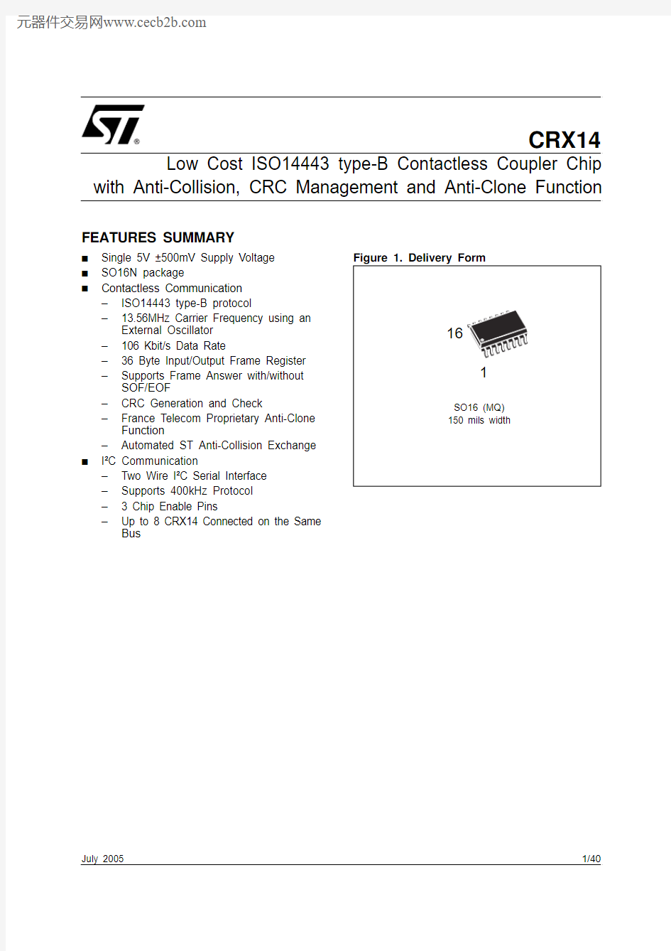
■Single 5V ±500mV Supply Voltage Array■SO16N package
■Contactless Communication
–ISO14443 type-B protocol
–13.56MHz Carrier Frequency using an
External Oscillator
–106 Kbit/s Data Rate
–36 Byte Input/Output Frame Register
–Supports Frame Answer with/without
SOF/EOF
–CRC Generation and Check
–France Telecom Proprietary Anti-Clone
Function
–Automated ST Anti-Collision Exchange
■I2C Communication
–Two Wire I2C Serial Interface
–Supports 400kHz Protocol
– 3 Chip Enable Pins
–Up to 8 CRX14 Connected on the Same
Bus
July 2005
1/40
CRX14
TABLE OF CONTENTS
FEATURES SUMMARY . . . . . . . . . . . . . . . . . . . . . . . . . . . . . . . . . . . . . . . . . . . . . . . . . . . . . . . . . . . . .1 Figure 1.Delivery Form . . . . . . . . . . . . . . . . . . . . . . . . . . . . . . . . . . . . . . . . . . . . . . . . . . . . . . . . . .1
SUMMARY DESCRIPTION. . . . . . . . . . . . . . . . . . . . . . . . . . . . . . . . . . . . . . . . . . . . . . . . . . . . . . . . . . .5
Figure 2.Logic Diagram . . . . . . . . . . . . . . . . . . . . . . . . . . . . . . . . . . . . . . . . . . . . . . . . . . . . . . . . . .5 Table 1.Signal Names . . . . . . . . . . . . . . . . . . . . . . . . . . . . . . . . . . . . . . . . . . . . . . . . . . . . . . . . . .5 Figure 3.Logic Block Diagram . . . . . . . . . . . . . . . . . . . . . . . . . . . . . . . . . . . . . . . . . . . . . . . . . . . . .6 Figure 4.SO Pin Connections . . . . . . . . . . . . . . . . . . . . . . . . . . . . . . . . . . . . . . . . . . . . . . . . . . . . .6
SIGNAL DESCRIPTION . . . . . . . . . . . . . . . . . . . . . . . . . . . . . . . . . . . . . . . . . . . . . . . . . . . . . . . . . . . . .7
Oscillator (OSC1, OSC2). . . . . . . . . . . . . . . . . . . . . . . . . . . . . . . . . . . . . . . . . . . . . . . . . . . . . . . . . .7 Antenna Output Driver (RF OUT). . . . . . . . . . . . . . . . . . . . . . . . . . . . . . . . . . . . . . . . . . . . . . . . . . . . .7 Antenna Input Filter (RF IN) . . . . . . . . . . . . . . . . . . . . . . . . . . . . . . . . . . . . . . . . . . . . . . . . . . . . . . . .7 Transmitter Reference Voltage (V REF) . . . . . . . . . . . . . . . . . . . . . . . . . . . . . . . . . . . . . . . . . . . . . . .7 Serial Clock (SCL). . . . . . . . . . . . . . . . . . . . . . . . . . . . . . . . . . . . . . . . . . . . . . . . . . . . . . . . . . . . . . .7 Serial Data (SDA) . . . . . . . . . . . . . . . . . . . . . . . . . . . . . . . . . . . . . . . . . . . . . . . . . . . . . . . . . . . . . . .7 Chip Enable (E0, E1, E2) . . . . . . . . . . . . . . . . . . . . . . . . . . . . . . . . . . . . . . . . . . . . . . . . . . . . . . . . .7 Power Supply (V CC, GND, GND_RF) . . . . . . . . . . . . . . . . . . . . . . . . . . . . . . . . . . . . . . . . . . . . . . . .7 Figure 5.CRX14 Application Schematic. . . . . . . . . . . . . . . . . . . . . . . . . . . . . . . . . . . . . . . . . . . . . .8 Figure 6.Maximum R L Value versus Bus Capacitance (C BUS) for an I2C Bus . . . . . . . . . . . . . . . .8
CRX14 REGISTERS . . . . . . . . . . . . . . . . . . . . . . . . . . . . . . . . . . . . . . . . . . . . . . . . . . . . . . . . . . . . . . . .9
Table 2.CRX14 Control Registers . . . . . . . . . . . . . . . . . . . . . . . . . . . . . . . . . . . . . . . . . . . . . . . . .9 Parameter Register (00h) . . . . . . . . . . . . . . . . . . . . . . . . . . . . . . . . . . . . . . . . . . . . . . . . . . . . . . . .9 Table 3.Parameter Register Bits Description . . . . . . . . . . . . . . . . . . . . . . . . . . . . . . . . . . . . . . . . .9 Input/Output Frame Register (01h) . . . . . . . . . . . . . . . . . . . . . . . . . . . . . . . . . . . . . . . . . . . . . . .10 Table 4.Input/Output Frame Register Description . . . . . . . . . . . . . . . . . . . . . . . . . . . . . . . . . . . .10 Authenticate Register (02h) . . . . . . . . . . . . . . . . . . . . . . . . . . . . . . . . . . . . . . . . . . . . . . . . . . . . .10 Slot Marker Register (03h) . . . . . . . . . . . . . . . . . . . . . . . . . . . . . . . . . . . . . . . . . . . . . . . . . . . . . .10 Table 5.Slot Marker Register Description . . . . . . . . . . . . . . . . . . . . . . . . . . . . . . . . . . . . . . . . . .11
CRX14 I2C PROTOCOL DESCRIPTION. . . . . . . . . . . . . . . . . . . . . . . . . . . . . . . . . . . . . . . . . . . . . . . .12
Table 6.Device Select Code. . . . . . . . . . . . . . . . . . . . . . . . . . . . . . . . . . . . . . . . . . . . . . . . . . . . .12 I2C Start Condition. . . . . . . . . . . . . . . . . . . . . . . . . . . . . . . . . . . . . . . . . . . . . . . . . . . . . . . . . . . . .12 I2C Stop Condition. . . . . . . . . . . . . . . . . . . . . . . . . . . . . . . . . . . . . . . . . . . . . . . . . . . . . . . . . . . . .12 I2C Acknowledge Bit (ACK). . . . . . . . . . . . . . . . . . . . . . . . . . . . . . . . . . . . . . . . . . . . . . . . . . . . . .12 I2C Data Input. . . . . . . . . . . . . . . . . . . . . . . . . . . . . . . . . . . . . . . . . . . . . . . . . . . . . . . . . . . . . . . . .12 Figure 7.I2C Bus Protocol . . . . . . . . . . . . . . . . . . . . . . . . . . . . . . . . . . . . . . . . . . . . . . . . . . . . . . .13 I2C Memory Addressing . . . . . . . . . . . . . . . . . . . . . . . . . . . . . . . . . . . . . . . . . . . . . . . . . . . . . . . .13 CRX14 I2C Write Operations. . . . . . . . . . . . . . . . . . . . . . . . . . . . . . . . . . . . . . . . . . . . . . . . . . . . .13 Figure 8.CRX14 I2C Write Mode Sequence . . . . . . . . . . . . . . . . . . . . . . . . . . . . . . . . . . . . . . . . .14 Figure 9.I2C Polling Flowchart using ACK . . . . . . . . . . . . . . . . . . . . . . . . . . . . . . . . . . . . . . . . . . .15 CRX14 I2C Read Operations. . . . . . . . . . . . . . . . . . . . . . . . . . . . . . . . . . . . . . . . . . . . . . . . . . . . .16
2/40
CRX14 Figure 10.CRX14 I2C Read Modes Sequences . . . . . . . . . . . . . . . . . . . . . . . . . . . . . . . . . . . . . . .16
APPLYING THE I2C PROTOCOL TO THE CRX14 REGISTERS. . . . . . . . . . . . . . . . . . . . . . . . . . . . .17
I2C Parameter Register Protocol . . . . . . . . . . . . . . . . . . . . . . . . . . . . . . . . . . . . . . . . . . . . . . . . .17 Figure 11.Host-to-CRX14 Transfer: I2C Write to Parameter Register . . . . . . . . . . . . . . . . . . . . . .17 Figure 12.CRX14-to-Host Transfer: I2C Random Address Read from Parameter Register . . . . . .17 Figure 13.CRX14-to-Host Transfer: I2C Current Address Read from Parameter Register . . . . . . .17 I2C Input/Output Frame Register Protocol . . . . . . . . . . . . . . . . . . . . . . . . . . . . . . . . . . . . . . . . .18 Figure 14.Host-to-CRX14 Transfer: I2C Write to Input/Output Frame Register for ISO14443B . . .18 Figure 15.CRX14-to-Host Transfer: I2C Random Address Read
from Input/Output Frame Register for ISO14443B . . . . . . . . . . . . . . . . . . . . . . . . . . . . .18 Figure 16.CRX14-to-Host Transfer: I2C Current Address Read
from I/O Frame Register for ISO14443B . . . . . . . . . . . . . . . . . . . . . . . . . . . . . . . . . . . .18 I2C Authenticate Register Protocol . . . . . . . . . . . . . . . . . . . . . . . . . . . . . . . . . . . . . . . . . . . . . . .19 I2C Slot Marker Register Protocol . . . . . . . . . . . . . . . . . . . . . . . . . . . . . . . . . . . . . . . . . . . . . . . .19 Figure 17.Host-to-CRX14 Transfer: I2C Write to Slot Marker Register . . . . . . . . . . . . . . . . . . . . . .19 Figure 18.CRX14-to-Host Transfer: I2C Random Address Read from Slot Marker Register . . . . .19 Figure 19.CRX14-to-Host Transfer: I2C Current Address Read from Slot Marker Register . . . . . .19 Addresses above Location 06h . . . . . . . . . . . . . . . . . . . . . . . . . . . . . . . . . . . . . . . . . . . . . . . . . .20
CRX14 ISO14443 TYPE-B RADIO FREQUENCY DATA TRANSFER . . . . . . . . . . . . . . . . . . . . . . . .21
Output RF Data Transfer from the CRX14 to the PICC (Request Frame). . . . . . . . . . . . . . . . .21 Figure 20.Wave Transmitted using ASK Modulation . . . . . . . . . . . . . . . . . . . . . . . . . . . . . . . . . . .21 Transmission Format of Request Frame Characters. . . . . . . . . . . . . . . . . . . . . . . . . . . . . . . . .21 Figure 21.CRX14 Request Frame Character Format . . . . . . . . . . . . . . . . . . . . . . . . . . . . . . . . . . .21 Table 7.CRX14 Request Frame Character Format . . . . . . . . . . . . . . . . . . . . . . . . . . . . . . . . . . .22 Request Start Of Frame . . . . . . . . . . . . . . . . . . . . . . . . . . . . . . . . . . . . . . . . . . . . . . . . . . . . . . . .22 Figure 22.Request Start Of Frame . . . . . . . . . . . . . . . . . . . . . . . . . . . . . . . . . . . . . . . . . . . . . . . . .22 Request End Of Frame . . . . . . . . . . . . . . . . . . . . . . . . . . . . . . . . . . . . . . . . . . . . . . . . . . . . . . . . .22 Figure 23.Request End Of Frame . . . . . . . . . . . . . . . . . . . . . . . . . . . . . . . . . . . . . . . . . . . . . . . . .22 Input RF Data Transfer from the PICC to the CRX14 (Answer Frame). . . . . . . . . . . . . . . . . . .23 Figure 24.Wave Received using BPSK Sub-carrier Modulation . . . . . . . . . . . . . . . . . . . . . . . . . . .23 Transmission Format of Answer Frame Characters . . . . . . . . . . . . . . . . . . . . . . . . . . . . . . . . .23 Answer Start Of Frame . . . . . . . . . . . . . . . . . . . . . . . . . . . . . . . . . . . . . . . . . . . . . . . . . . . . . . . . .24 Figure 25.Answer Start Of Frame . . . . . . . . . . . . . . . . . . . . . . . . . . . . . . . . . . . . . . . . . . . . . . . . . .24 Answer End Of Frame. . . . . . . . . . . . . . . . . . . . . . . . . . . . . . . . . . . . . . . . . . . . . . . . . . . . . . . . . .24 Figure 26.Answer End Of Frame . . . . . . . . . . . . . . . . . . . . . . . . . . . . . . . . . . . . . . . . . . . . . . . . . .24 Transmission Frame. . . . . . . . . . . . . . . . . . . . . . . . . . . . . . . . . . . . . . . . . . . . . . . . . . . . . . . . . . .25 Figure 27.Example of a Complete Transmission Frame . . . . . . . . . . . . . . . . . . . . . . . . . . . . . . . .25 CRC. . . . . . . . . . . . . . . . . . . . . . . . . . . . . . . . . . . . . . . . . . . . . . . . . . . . . . . . . . . . . . . . . . . . . . . . .25 Figure 28.CRC Transmission Rules . . . . . . . . . . . . . . . . . . . . . . . . . . . . . . . . . . . . . . . . . . . . . . . .25
TAG ACCESS USING THE CRX14 COUPLER . . . . . . . . . . . . . . . . . . . . . . . . . . . . . . . . . . . . . . . . . .26
Standard TAG Command Access Description. . . . . . . . . . . . . . . . . . . . . . . . . . . . . . . . . . . . . .26 Figure 29.Standard TAG Command: Request Frame Transmission. . . . . . . . . . . . . . . . . . . . . . . .26 Figure 30.Standard TAG Command: Answer Frame Reception. . . . . . . . . . . . . . . . . . . . . . . . . . .26
3/40
CRX14
4/40Figure 31.Standard TAG Command: Complete TAG Access Description . . . . . . . . . . . . . . . . . . .27 Anti-Collision TAG Sequence. . . . . . . . . . . . . . . . . . . . . . . . . . . . . . . . . . . . . . . . . . . . . . . . . . . .27 Figure 32.Anti-Collision ST short range memory Sequence (1) . . . . . . . . . . . . . . . . . . . . . . . . . . .28 Figure 33.Anti-Collision ST short range memory Sequence Continued . . . . . . . . . . . . . . . . . . . . .29
MAXIMUM RATING. . . . . . . . . . . . . . . . . . . . . . . . . . . . . . . . . . . . . . . . . . . . . . . . . . . . . . . . . . . . . . . .30 Table 8.Absolute Maximum Ratings. . . . . . . . . . . . . . . . . . . . . . . . . . . . . . . . . . . . . . . . . . . . . . .30
DC AND AC PARAMETERS. . . . . . . . . . . . . . . . . . . . . . . . . . . . . . . . . . . . . . . . . . . . . . . . . . . . . . . . .31
Table 9.I2C AC Measurement Conditions. . . . . . . . . . . . . . . . . . . . . . . . . . . . . . . . . . . . . . . . . . .31 Figure 34.I2C AC Testing I/O Waveform . . . . . . . . . . . . . . . . . . . . . . . . . . . . . . . . . . . . . . . . . . . . .31 Table 10.I2C Input Parameters(1,2) . . . . . . . . . . . . . . . . . . . . . . . . . . . . . . . . . . . . . . . . . . . . . . . .31 Table 11.I2C DC Characteristics . . . . . . . . . . . . . . . . . . . . . . . . . . . . . . . . . . . . . . . . . . . . . . . . . .32 Figure 35.I2C AC Waveforms . . . . . . . . . . . . . . . . . . . . . . . . . . . . . . . . . . . . . . . . . . . . . . . . . . . . .32 Table 12.I2C AC Characteristics . . . . . . . . . . . . . . . . . . . . . . . . . . . . . . . . . . . . . . . . . . . . . . . . . .33 Figure 36.CRX14 Synchronous Timing . . . . . . . . . . . . . . . . . . . . . . . . . . . . . . . . . . . . . . . . . . . . .34 Table 13.RF OUT AC Characteristics. . . . . . . . . . . . . . . . . . . . . . . . . . . . . . . . . . . . . . . . . . . . . . . .35 Table 14.RF IN AC Characteristics . . . . . . . . . . . . . . . . . . . . . . . . . . . . . . . . . . . . . . . . . . . . . . . . .35
PACKAGE MECHANICAL . . . . . . . . . . . . . . . . . . . . . . . . . . . . . . . . . . . . . . . . . . . . . . . . . . . . . . . . . .36
Figure 37.SO16 Narrow - 16 lead Plastic Small Outline, 150 mils body width, Package Outline . .36 Table 15.SO16 Narrow - 16 lead Plastic Small Outline, 150 mils body width,
Package Mechanical Data. . . . . . . . . . . . . . . . . . . . . . . . . . . . . . . . . . . . . . . . . . . . . . . .36
PART NUMBERING . . . . . . . . . . . . . . . . . . . . . . . . . . . . . . . . . . . . . . . . . . . . . . . . . . . . . . . . . . . . . . .37 Table 16.Ordering Information Scheme . . . . . . . . . . . . . . . . . . . . . . . . . . . . . . . . . . . . . . . . . . . . .37
APPENDIX A.ISO14443 TYPE B CRC CALCULATION . . . . . . . . . . . . . . . . . . . . . . . . . . . . . . . . . . .38
REVISION HISTORY. . . . . . . . . . . . . . . . . . . . . . . . . . . . . . . . . . . . . . . . . . . . . . . . . . . . . . . . . . . . . . .39 Table 17.Document Revision History. . . . . . . . . . . . . . . . . . . . . . . . . . . . . . . . . . . . . . . . . . . . . . .39
CRX14 SUMMARY DESCRIPTION
The CRX14 is a contactless coupler that is compli-ant with the short range ISO14443 type-B stan-dard. It is controlled using the two wire I2C bus. The CRX14 generates a 13.56MHz signal on an external antenna. Transmitted data are modulated using Amplitude Shift Keying (ASK). Received data are demodulated from the PICC (Proximity in-tegrated Coupling Card) load variation signal, in-duced on the antenna, using Bit Phase Shift Keying (BPSK) of a 847kHz sub-carrier. The Transmitted ASK wave is 10% modulated. The Data transfer rate between the CRX14 and the PICC is 106 Kbit/s in both transmission and recep-tion modes.
The CRX14 follows the ISO14443 type-B recom-mendation for Radio frequency power and signal interface.
The CRX14 is specifically designed for short range applications that need disposable, or secure and re-usable, products.
The CRX14 includes an automated anti-collision mechanism that allows it to detect and select any ST short range memories that are present at the same time within its range. The anti-collision mechanism is based on the STMicroelectronics probabilistic scanning method.
The CRX14 provides an anti-clone function, from FRANCE TELECOM, which allows the authentication of the ST short range memories. Using the CRX14 single chip coupler, therefore, it is easy to design a reader, with authentication ca-pability and to build an end application with a high level of security at low cost.
The CRX14 provides a complete analog interface, compliant with the ISO14443 type-B recommendations for Radio-Frequency power and signal interfacing. With it, any ISO14443 type-B PICC products can be powered and have their data transmission controlled via a simple antenna. The CRX14 is fabricated in STMicroelectronics High Endurance Single Poly-silicon CMOS tech-nology.
The CRX14 is organized as 4 different blocks (see Figure 3.):
■The I2C bus controller. It handles the serial connection with the application host. It is
compliant with the 400kHz I2C bus
specification, and controls the read/write
access to all the CRX14 registers.
■The RAM buffer. It is bi-directional. . It stores all the request frame Bytes to be transmitted to the PICC, and all the received Bytes sent by the PICC on the answer frame.
■The transmitter. It powers the PICCs by generating a 13.56MHz signal on an external
antenna. The resulting field is 10% modulated using ASK (amplitude shift keying) for
outgoing data.
■The receiver. It demodulates the signal generated on the antenna by the load variation of the PICC. The resulting signal is decoded by a 847kHz BPSK (binary phase shift keying) sub-carrier decoder.
The CRX14 is designed to be connected to a digi-tal host (Microcontroller or ASIC). This host has to manage the entire communication protocol in both transmit and receive modes, through the I2C serial bus.
Table 1. Signal Names
RF OUT Antenna Output Driver
RF IN Antenna Input Filter
OSC1Oscillator Input
OSC2Oscillator Output
E0, E1, E2Chip Enable Inputs
SDA I2C Bi-Directional Data
SCL I2C Clock
V CC Power Supply
GND Ground
V REF Transmitter Reference Voltage
GND_RF Ground for RF circuitry
5/40
CRX14
6/40
CRX14 SIGNAL DESCRIPTION
See Figure 2., and Table 1., for an overview of the signals connected to this device.
Oscillator (OSC1, OSC2).The OSC1 and OSC2 pins are internally connected to the on-chip oscil-lator circuit. The OSC1 pin is the input pin, the OSC2 is the output pin. For correct operation of the CRX14, it is required to connect a 13.56MHz quartz crystal across OSC1 and OSC2. If an exter-nal clock is used, it must be connected to OSC1 and OSC2 must be left open.
Antenna Output Driver (RF OUT).The Antenna Output Driver pin, RF OUT, generates the modulat-ed 13.56MHz signal on the antenna. Care must be taken as it will not withstand a short-circuit.
RF OUT has to be connected to the antenna circuit-ry as shown in Figure 5. The LRC antenna circuitry must be connected across the RF OUT pin and GND.
Antenna Input Filter (RF IN).The antenna input filter of the CRX14, RF IN, has to be connected to the external antenna through an adapter circuit, as shown in Figure 5.
The input filter demodulates the signal generated on the antenna by the load variation of the PICC. The resulting signal is then decoded by the 847kHz BPSK decoder.
Transmitter Reference Voltage (V REF).The Transmitter Reference Voltage input, V REF, pro-vides a reference voltage used by the output driver for ASK modulation.
The Transmitter Reference Voltage input should be connected to an external capacitor, as shown in Figure 5.
Serial Clock (SCL).The SCL input pin is used to strobe all I2C data in and out of the CRX14. In ap-plications where this line is used by slave devices to synchronize the bus to a slower clock, the mas-ter must have an open drain output, and a pull-up resistor must be connected from the Serial Clock (SCL) to V CC. ( Figure 6. indicates how the value of the pull-up resistor can be calculated).
In most applications, though, this method of syn-chronization is not employed, and so the pull-up resistor is not necessary, provided that the master has a push-pull (rather than open drain) output.
Serial Data (SDA).The SDA signal is bi-direc-tional. It is used to transfer I2C data in and out of the CRX14. It is an open drain output that may be wire-OR’ed with other open drain or open collector signals on the bus. A pull-up resistor must be con-nected from Serial data (SDA) to V CC. (Figure 6. indicates how the value of the pull-up resistor can be calculated).
Chip Enable (E0, E1, E2).The Chip Enable in-puts E0, E1, E2 are used to set and reset the value on the three least significant bits (b3, b2, b1) of the 7-bit I2C Device Select Code. They are used for hardwired addressing, allowing up to eight CRX14 devices to be addressed on the same I2C bus. These inputs may be driven dynamically or tied to V CC or GND to establish the Device Select Code (note that the V IL and V IH levels for the inputs are CMOS compatible, not TTL compatible).
When left open, E0, E1 and E2 are internally read at the logic level 0 due to the internal pull-down re-sistors connected to each inputs.
Power Supply (V CC, GND, GND_RF).Power is supplied to the CRX14 using the V CC, GND and GND_RF pins.
V CC is the Power Supply pin that supplies the pow-er (+5V) for all CRX14 operations.
The GND and GND_RF pins are ground connec-tions. They must be connected together. Decoupling capacitors should be connected be-tween the V CC Supply Voltage pin, the GND Ground pin and the GND_REF Ground pin to filter the power line, as shown in Figure 5.
7/40
CRX14
2
8/40
9/40
CRX14
CRX14 REGISTERS
The CRX14 chip coupler contains six volatile reg-isters. It is entirely controlled, at both digital and analog level, using the four registers listed below and shown in Table 2.:■Parameter Register ■Input/Output Frame Register ■Authentication Register ■Slot Marker Register The other 2 registers are located at addresses 04h and 05h. They are “ST Reserved”, and must not be used in end-user applications.
In the I2C protocol, all data Bytes are transmitted Most Significant Byte first, with each Byte transmit-ted Most significant bit first.
Table 2. CRX14 Control Registers
Parameter Register (00h)
The Parameter Register is an 8-bit volatile register used to configure the CRX14, and thus, to custom-ize the circuit behavior. The Parameter Register is located at the I2C address 00h and it is accessible in I2C Read and Write modes. Its default value,00h, puts the CRX14 in standard ISO14443 type-B configuration.
Table 3. Parameter Register Bits Description
Note:RFU = Reserved for Future Use.
Address Length Access Purpose
00h
Parameter Register
1 Byte
W Set parameter register R Read parameter register
01h Input/output Frame Register 36 Bytes
W Store and send request frame to the PICC.
Wait for PICC answer frame
R
Transfer PICC answered frame data to Host 02h
Authenticate Register
NA
W Start the Authentication process R Get the Authentication status
03h Slot Marker Register 1 Byte
W Launch the automated anti-collision process from Slot_0 to Slot_15R
Return data FFh
04h ST Reserved NA R and W ST Reserved. Must not be used 05h
ST Reserved
NA
R and W ST Reserved. Must not be used
Bit Control
Value Description
b 0Frame Standard 0 ISO14443 type-B frame management
1RFU b 1RFU
0Not used
b 2Answer Frame Format 0Answer PICC Frames are delimited by SOF and EOF 1Answer PICC Frames do not provide SOF and EOF delimiters b 3ASK Modulation Depth 010% ASK modulation depth mode 1RFU
b 4Carrier Frequency
013.56MHz carrier on RF OUT is OFF 1
13.56MHz carrier on RF OUT is ON
b 5t WDG
Answer delay watchdog b5=0, b6=0: Watchdog time-out = 500μs to be used for read
b5=0, b6=1: Watchdog time-out = 5ms to be used for authentication b5=1, b6=0: Watchdog time-out = 10ms to be used for write
b5=1, b6=1: Watchdog time-out = 309ms to be used for MCU timings b 6b 7
RFU
Not used
CRX14
10/40
Input/Output Frame Register (01h)
The Input/Output Frame Register is a 36-Byte buffer that is accessed serially from Byte 0 through to Byte 35 (see Table 4.). It is located at the I2C ad-dress 01h.
The Input/Output Frame Register is the buffer in which the CRX14 stores the data Bytes of the re-quest frame to be sent to the PICC. It automatical-ly stores the data Bytes of the answer frame received from the PICC. The first Byte (Byte 0) of the Input/Output Frame Register is used to store the frame length for both transmission and recep-tion.
When accessed in I2C Write mode , the register stores the request frame Bytes that are to be transmitted to the PICC. Byte 0 must be set with the request frame length (in Bytes) and the frame is stored from Byte 1 onwards. At the end of the transmission, the 16-bit CRC is automatically add-ed. After the transmission, the CRX14 wait for the PICC to send back an answer frame. When cor-rectly decoded, the PICC answer frame Bytes are stored in the Input/Output Frame Register from Byte 1 onwards. Byte 0 stores the number of Bytes received from the PICC.
When accessed in I2C Read mode, the Input/Out-put Register sends back the last PICC answer frame Bytes, if any, with Byte 0 transmitted first.The 16-bit CRC is not stored, and it is not sent back on the I2C bus.
The Input/Output Frame Register is set to all 00h between transmission and reception. If there is no answer from the PICC, Byte 0 is set to 00h. In the case of a CRC error, Byte 0 is set to FFh, and the data Bytes are discarded and not appended in the register.
The CRX14 Input/Output Frame Register is so de-signed as to generate all the ST short range mem-ory command frames. It can also generate all standardized ISO14443 type-B command frames like REQB, SLOT-MARKER, ATTRIB, HALT, and get all the answers like ATQB, or answer to AT-TRIB. All ISO14443 type-B compliant PICCs can be accessed by the CRX14 provided that their data frame exchange is not longer than 35 Bytes in both request and answer.
Table 4. Input/Output Frame Register Description
Authenticate Register (02h)
The Authenticate Register is used to trigger the complete authentication exchange between the CRX14 and the secured ST short range memory.It is located at the I2C address 02h.
The Authentication system is based on a propri-etary challenge/response mechanism that allows the application software to authenticate a secured ST short range memory of the SRXxxx family. A reader designed with the CRX14 can check the authenticity of a memory device and protect the application system against silicon copies or emu-lators.
A complete description of the Authentication sys-tem is available under Non Disclosure Agreement (NDA) with STMicroelectronics. For more details about this CRX14 function, please contact the nearest STMicroelectronics sales office.Slot Marker Register (03h)
The slot Marker Register is located at the I2C ad-dress 03h. It is used to trigger an automated anti-
collision sequence between the CRX14 and any ST short range memory present in the electromag-netic field. With one I2C access, the CRX14launches a complete stream of commands starting from PCALL16(), SLOT_MARKER(1),SLOT_MARKER(2) up to SLOT_MARKER(15),and stores all the identified Chip_IDs into the In-put/Output Frame Register (I2C address 01h). This automated anti-collision sequence simplifies the host software development and reduces the time needed to interrogate the 16 slots of the ST-Microelectronics anti-collision mechanism.
When accessed in I2C Write mode, the Slot Marker Register starts generating the sequence of anti-collision commands. After each command, the CRX14 wait for the ST short range memory an-swer frame which contains the Chip_ID. The valid-ity of the answer is checked and stored into the corresponding Status Slot Bit (Byte 1 and Byte 2as described in Table 6.). If the answer is correct,the Status Slot Bit is set to ‘1’ and the Chip_ID is stored into the corresponding Slot_Register. If no answer is detected, the Status Slot Bit is set to ‘0’,and the corresponding Slot_Register is set to 00h.
Byte 0Byte 1Byte 2Byte 3
...
Byte 34
Byte 35Frame Length
First data Byte
Second data Byte
Last data Byte
<------------- Request and Answer Frame Bytes exchanged on the RF ------------->
00h No Byte transmitted FFh CRC Error
xxh Number of transmitted Bytes
CRX14
If a CRC error is detected, the Status Slot Bit is set to ‘0’, and the corresponding Slot_Register is set to FFh.
Each time the Slot Marker Register is accessed in I2C Write mode, Byte 0 of the Input/Output Frame Register is set to 18, Bytes 1 and 2 provide Status Bits Slot information, and Bytes 3 to 18 store the corresponding Chip_ID or error code.
The Slot Marker Register cannot be accessed in I2C Read mode. All the anti-collision data can be accessed by reading the Input/Output Frame Reg-ister at the I2C address 01h.
Table 5. Slot Marker Register Description
b7b6b5b4b3b2b1b0 Byte 0Number of stored Bytes: fixed to 18
Byte 1Status Slot
Bit 7
Status Slot
Bit 6
Status Slot
Bit 5
Status Slot
Bit 4
Status Slot
Bit 3
Status Slot
Bit 2
Status Slot
Bit 1
Status Slot
Bit 0
Byte 2Status Slot
Bit 15
Status Slot
Bit 14
Status Slot
Bit 13
Status Slot
Bit 12
Status Slot
Bit 11
Status Slot
Bit 10
Status Slot
Bit 9
Status Slot
Bit 8
Byte 3Slot_Register 0 = Chip_ID value detected in Slot 0
Byte 4Slot_Register 1 = Chip_ID value detected in Slot 1
Byte 5Slot_Register 2 = Chip_ID value detected in Slot 2
Byte 6Slot_Register 3 = Chip_ID value detected in Slot 3
Byte n.....
Byte 17Slot_Register 14 = Chip_ID value detected in Slot 14
Byte 18Slot_Register 15 = Chip_ID value detected in Slot 15
Status bit value description:
1: No error detected. The Chip_ID stored in the Slot register is valid.
0: Error detected
- Slot register = 00h: No answer frame detected from ST short range memory
- Slot register = FFh: Answer Frame detected with CRC error. Collision may have occurred
11/40
CRX14
12/40
CRX14 I2C PROTOCOL DESCRIPTION
The CRX14 is compatible with the I2C serial bus memory standard, which is a two-wire serial inter-face that uses a bi-directional data bus and serial clock.
The CRX14 has a pre-programmed, 4-bit identifi-cation code, ’1010’ (as shown in Table 6.), that corresponds to the I2C bus definition. With this code and the three Chip Enable inputs (E2, E1,E0) up to eight CRX14 devices can be connected to the I2C bus, and selected individually.
The CRX14 behaves as a slave device in the I2C protocol, with all CRX14 operations synchronized to the serial clock.
I2C Read and Write operations are initiated by a START condition, generated by the bus master.The START condition is followed by the Device terminated by an acknowledge bit. The Device Se-lect Code consists of seven bits (as shown in Ta-ble 6.):■the Device Code (first four bits)■plus three bits corresponding to the states of
the three Chip Enable inputs, E2, E1 and E0, respectively When data is written to the CRX14, the device in-serts an acknowledge bit (9th bit) after the bus master’s 8-bit transmission.
When the bus master reads data, it also acknowl-edges the receipt of the data Byte by inserting an acknowledge bit (9th bit).
Data transfers are terminated by a STOP condition after an ACK for Write, or after a NoACK for Read.The CRX14 supports the I2C protocol, as summa-rized in Figure 7.
Any device that sends data on to the bus, is de-fined as a transmitter, and any device that reads the data, as a receiver.
The device that controls the data transfer is known as the master, and the other, as the slave. A data transfer can only be initiated by the master, which also provides the serial clock for synchronization.The CRX14 is always a slave device in all I2C com-munications. All data are transmitted Most Signifi-cant Bit (MSB) first.
Table 6. Device Select Code
I2C Start Condition
START is identified by a High-to-Low transition of the Serial Data line, SDA, while the Serial Clock,SCL, is stable in the High state. A START condi-tion must precede any data transfer command.The CRX14 continuously monitors the SDA and SCL lines for a START condition (except during Radio Frequency data exchanges), and will not re-spond unless one is sent.I2C Stop Condition
STOP is identified by a Low-to-High transition of the Serial Data line, SDA, while the Serial Clock,SCL, is stable in the High state.
A STOP condition terminates communications be-tween the CRX14 and the bus master.
A STOP condition at the end of an I2C Read com-mand, after (and only after) a NoACK, forces the CRX14 into its stand-by state.
A STOP condition at the end of an I2C Write com-mand triggers the Radio Frequency data ex-change between the CRX14 and the PICC.I2C Acknowledge Bit (ACK)
An acknowledge bit is used to indicate a success-ful data transfer on the I2C bus.
The bus transmitter, either master or slave, releas-es the Serial Data line, SDA, after sending 8 bits of data. During the 9th clock pulse the receiver pulls the SDA line Low to acknowledge the receipt of the 8 data bits.I2C Data Input
During data input, the CRX14 samples the SDA bus signal on the rising edge of the Serial Clock,SCL. For correct device operation, the SDA signal must be stable during the Low-to-High Serial Clock transition, and the data must change only when the SCL line is Low
Device Code
Chip Enable
RW b7
b6b5b4b3b2b1b0CRX14 Select 1
1
E2
E1
E0
RW
CRX14
I2C Memory Addressing
To start up communication with the CRX14, the bus master must initiate a START condition. Then, the bus master sends 8 bits (with the most signifi-cant bit first) on the Serial Data line, SDA. These bits consist of the Device Select Code (7 bits) plus According to the I2C bus definition, the seven most significant bits of the Device Select Code are the Device Type Identifier. For the CRX14, these bits are defined as shown in Table 6.
The 8th bit is the Read/Write bit (RW). It is set to ‘1’ for I2C Read, and to ‘0’ for I2C Write operations. If the data sent by the bus master matches the De-vice Select Code of a CRX14 device, the corre-sponding device returns an acknowledgment on the SDA bus during the 9th bit time.
The CRX14 devices whose Device Select Codes do not correspond to the data sent, generate a No-ACK. They deselect themselves from the bus and go into stand-by mode.
CRX14 I2C Write Operations
The bus master sends a START condition, fol-to ’0’. The CRX14 that corresponds to the Device Select Code, acknowledges and waits for the bus master to send the Byte address of the register that is to be written to. After receipt of the address, the CRX14 returns another ACK, and waits for the bus master to send the data Bytes that are to be written.
In the CRX14 I2C Write mode, the bus master may sends one or more data Bytes depending on the selected register.
The CRX14 replies with an ACK after each data Byte received. The bus master terminates the transfer by generating a STOP condition.
13/40
CRX14
14/40
The STOP condition at the end of a Write access to the Input/Output Frame, Authenticate or Anti-Collision Register, causes the Radio Frequency data exchange between the CRX14 and the PICC to be started.
During the Radio Frequency data exchange, the CRX14 disconnects itself from the I2C bus. The time (t RFEX ) needed to complete the exchange is not fixed as it depends on the PICC command for-mat. To know when the exchange is complete, the bus master uses an ACK polling sequence as shown in Figure 9. It consists of the following:
■Initial condition: a Radio Frequency data exchange is in progress.
■
Step 1: the master issues a START condition followed by the first Byte of the new instruction (Device Select Code plus R/W bit).
■
Step 2: if the CRX14 is busy, no ACK is
returned and the master goes back to Step 1. If the CRX14 has completed the Radio
Frequency data exchange, it responds with an ACK, indicating that it is ready to receive the second part of the next instruction (the first Byte of this instruction being sent during Step 1).
CRX14
15/40
CRX14
16/40
CRX14 I2C Read Operations
To send a Read command, the bus master sends a START condition, followed by a Device Select The CRX14 that corresponds to the Device Select Code acknowledges and outputs the first data Byte of the addressed register.
To select a specific register, a dummy Write com-mand must first be issued, giving an address Byte but no data Bytes, as shown in the bottom half of Figure 10. This causes the new address to be stored in the internal address pointer, for use by the Read command that immediately follows the dummy Write command.
In the I2C Read mode, the CRX14 may read one or more data Bytes depending on the selected reg-ister. The bus master has to generate an ACK af-ter each data Byte to read all the register data in a continuous stream. Only the last data Byte should not be followed by an ACK. The master then termi-nates the transfer with a STOP condition, as shown in Figure 10.
After reading each Byte, the CRX14 waits for the master to send an ACK during the 9th bit time. If the master does not return an ACK within this time,the CRX14 terminates the data transfer and switches to stand-by mode.
CRX14 APPLYING THE I2C PROTOCOL TO THE CRX14 REGISTERS
I2C Parameter Register Protocol
Figure 11. shows how new data is written to the Parameter Register. The new value becomes ac-tive after the I2C STOP condition.
Figure 12. shows how to read the Parameter Reg-ister contents. The CRX14 sends and re-sends the Parameter Register contents until it receives a NoACK from the I2C Host.
The CRX14 supports the I2C Current Address and Random Address Read modes. The Current Ad-dress Read mode can be used if the previous command was issued to the register where the Read is to take place.
17/40
CRX14
18/40
I2C Input/Output Frame Register Protocol
Figure 14. shows how to store a PICC request frame command of N Bytes into the Input/Output Frame Register.
After the I2C STOP condition, the request frame is RF transmitted in the ISO14443 type-B format.The CRX14 then waits for the PICC answer frame which will also be stored in the Input/Output Frame Register. The request frame is over-written by the answer frame.
Figure 15. shows how to read an N -Byte PICC an-swer frame.
The two CRC Bytes generated by the PICC are not stored.
The CRX14 continues to output data Bytes until a NoACK has been generated by the I2C Host, and received by the CRX14. After all 36 Bytes have been output, the CRX14 “rolls over”, and starts outputting from the start of the Input/Output Frame Register again.
The CRX14 supports the I2C Current Address and Random Address Read modes. The Current Ad-dress Read mode can be used if the previous command was issued to the register where the Read is to take place.
Figure 15. CRX14-to-Host Transfer: I2C Random Address Read
Figure 16. CRX14-to-Host Transfer: I2C Current Address Read
CRX14
I2C Authenticate Register Protocol
For information please contact your nearest STMi-croelectronics sales office.
I2C Slot Marker Register Protocol
An I2C Write command to the Slot Marker Register generates an automated sixteen-command loop (See Figure 17. for a description of the command). All the answers from the ST short range memory devices that are detected, are written in the Input/ Output Frame Register.Read from the I2C Slot Marker Register is not sup-ported by the CRX14. If the I2C Host tries to read the Slot Marker Register, the CRX14 will return the data value FFh in both Random Address and Cur-rent Address Read modes until NoACK is generat-ed by the I2C Host.
The result of the detection sequence is stored in the Input/Output Frame Register. This Register can be read by the host by using I2C Random Ad-dress Read.
19/40
CRX14
20/40
Addresses above Location 06h
In I2C Write mode, when the CRX14 receives the 8-bit register address, and the address is above lo-cation 06h, the device does not acknowledge (NoACK) and deselects itself from the bus. The Serial Data line, SDA, stays at logic ‘1’ (pull-up re-sistor), and the I2C Host receives a NoACK during
the 9th bit time. The SDA line stays High until the STOP condition is issued.
In the I2C Current and Random Address Read modes, when the CRX14 receives the 8-bit regis-ter address, and the address is above location 06h, the device does not acknowledge the Device Select Code after the START condition, and dese-lects itself from the bus.