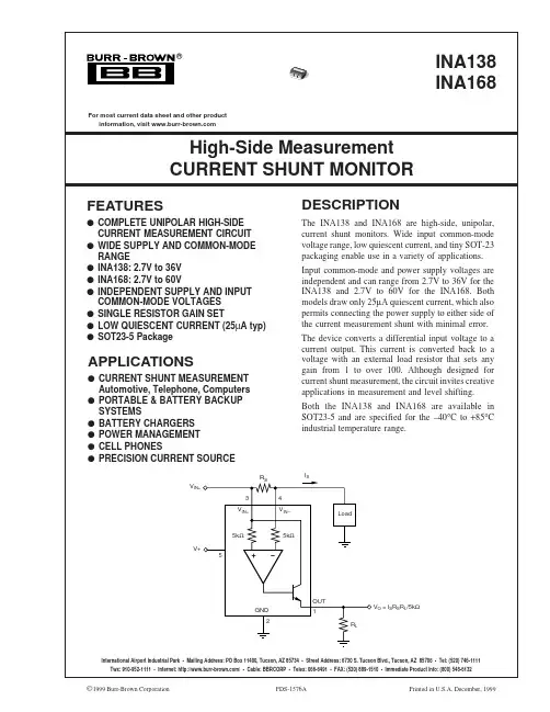
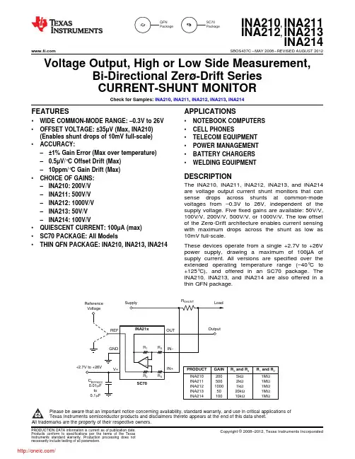
INA219中文资料
- 格式:pdf
- 大小:898.92 KB
- 文档页数:33
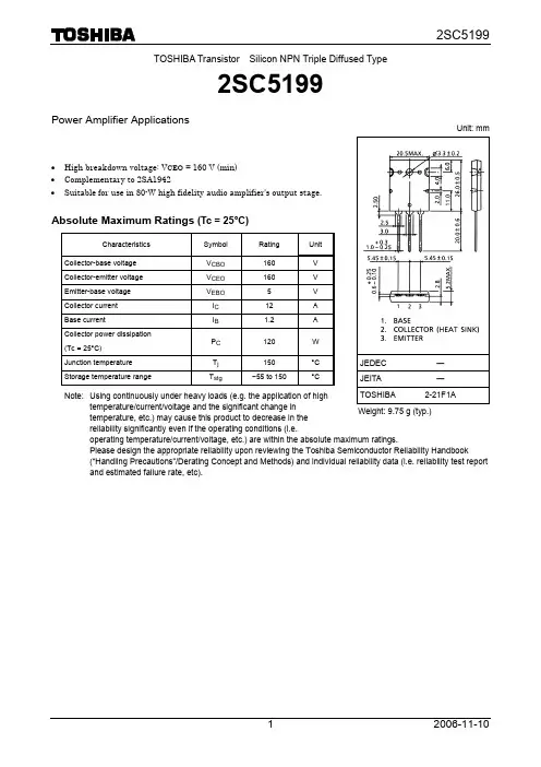
TOSHIBA Transistor Silicon NPN Triple Diffused Type2SC5199Power Amplifier Applications• High breakdown voltage: V CEO = 160 V (min) • Complementary to 2SA1942• Suitable for use in 80-W high fidelity audio amplifier’s output stage.Absolute Maximum Ratings (Tc = 25°C)Characteristics Symbol Rating UnitCollector-base voltage V CBO 160 V Collector-emitter voltage V CEO 160 V Emitter-base voltage V EBO 5 V Collector current I C 12 A Base currentI B 1.2 A Collector power dissipation (Tc = 25°C)P C 120 WJunction temperature T j 150 °C Storage temperature rangeT stg−55 to 150°CNote: Using continuously under heavy loads (e.g. the application of high temperature/current/voltage and the significant change intemperature, etc.) may cause this product to decrease in the reliability significantly even if the operating conditions (i.e.operating temperature/current/voltage, etc.) are within the absolute maximum ratings.Please design the appropriate reliability upon reviewing the Toshiba Semiconductor Reliability Handbook(“Handling Precautions”/Derating Concept and Methods) and individual reliability data (i.e. reliability test report and estimated failure rate, etc).Unit: mmJEDEC ― JEITA―TOSHIBA 2-21F1A Weight: 9.75 g (typ.)Electrical Characteristics (Tc = 25°C)Characteristics Symbol TestCondition MinTyp.Max UnitCollector cut-off current I CBO V CB = 160 V, I E = 0 ―― 5.0 μAEmitter cut-off current I EBO V EB = 5 V, I C = 0 ―― 5.0 μA Collector-emitter breakdown voltage V (BR) CEO I C = 50 mA, I B = 0 160 ―― Vh FE (1)(Note)V CE = 5 V, I C = 1 A 55 ― 160DC current gainh FE (2)V CE = 5 V, I C = 6 A 35 74 ―Collector-emitter saturation voltage V CE (sat) I C = 8 A, I B = 0.8 A ― 0.35 2.5 V Base-emitter voltage V BE V CE = 5 V, I C = 6 A ― 1.0 1.5 V Transition frequency f T V CE = 5 V, I C = 1 A ― 30 ― MHz Collector output capacitance C ob V CB = 10 V, I E = 0, f = 1 MHz ― 170 ― pF Note: h FE (1) classification R: 55 to 110, O: 80 to 160Markinglead (Pb)-free finish.Collector current I C (A)C o l l e c t o r -e m i t t e r s a t u r a t i o nv o l t ag e VC E (s a t ) (V )V CE (sat) – I CCollector-emitter voltage V CE (V)I C – V CEC o l l e c t orc u r r e n t IC (A )I C – V BECollector current I C (A)h FE – ICD C c u r re n t g a i n h F EBase-emitter voltage V BE (V)Co l l ect or cu r re nt I C (A)Collector-emitter voltage V CE (V)C o l l e c t o r c u r r e n t I C (A )Safe Operating Area0.1 1 0.0110210 30 100 3003RESTRICTIONS ON PRODUCT USE20070701-EN •The information contained herein is subject to change without notice.•TOSHIBA is continually working to improve the quality and reliability of its products. Nevertheless, semiconductor devices in general can malfunction or fail due to their inherent electrical sensitivity and vulnerability to physical stress. It is the responsibility of the buyer, when utilizing TOSHIBA products, to comply with the standards of safety in making a safe design for the entire system, and to avoid situations in which a malfunction or failure of such TOSHIBA products could cause loss of human life, bodily injury or damage to property.In developing your designs, please ensure that TOSHIBA products are used within specified operating ranges as set forth in the most recent TOSHIBA products specifications. Also, please keep in mind the precautions and conditions set forth in the “Handling Guide for Semiconductor Devices,” or “TOSHIBA Semiconductor Reliability Handbook” etc.• The TOSHIBA products listed in this document are intended for usage in general electronics applications (computer, personal equipment, office equipment, measuring equipment, industrial robotics, domestic appliances, etc.).These TOSHIBA products are neither intended nor warranted for usage in equipment that requires extraordinarily high quality and/or reliability or a malfunction or failure of which may cause loss of human life or bodily injury (“Unintended Usage”). Unintended Usage include atomic energy control instruments, airplane or spaceship instruments, transportation instruments, traffic signal instruments, combustion control instruments, medical instruments, all types of safety devices, etc.. Unintended Usage of TOSHIBA products listed in his document shall be made at the customer’s own risk.•The products described in this document shall not be used or embedded to any downstream products of which manufacture, use and/or sale are prohibited under any applicable laws and regulations.• The information contained herein is presented only as a guide for the applications of our products. No responsibility is assumed by TOSHIBA for any infringements of patents or other rights of the third parties which may result from its use. No license is granted by implication or otherwise under any patents or other rights of TOSHIBA or the third parties.• Please contact your sales representative for product-by-product details in this document regarding RoHS compatibility. Please use these products in this document in compliance with all applicable laws and regulations that regulate the inclusion or use of controlled substances. Toshiba assumes no liability for damage or losses occurring as a result of noncompliance with applicable laws and regulations.。
Features Array•Single Chip All-in-one Design–MIDI Control Processor, Serial and Parallel Interface–Synthesis, General MIDI Wavetable Implementation–General MIDI Compatible Effects: Reverb + Chorus–Spatial Effect–4-band Stereo Equalizer–Stereo DAC. DR: 86 dB min, THD+N: -80 dB max•State of the art Synthesis for Products Providing Best Quality for Price –64-voice Polyphony (without effects)–38-voice Polyphony + Effects–On-chip CleanWave™ Wavetable Data, Firmware, RAM Delay Lines•Audio Stereo Line Output•Typical Applications: Battery Operated Musical Keyboards, Portable Phones, Karaokes •QFN44 (7mm x 7mm) Package: Small Footprint, Small Pin Count•Low Power–75 mW typ. Operating–Single 3.3V or Single 1.8V Power Supply–Built-in Power Switch and 3.3V to 1.8V Regulator1.Typical Hardware ConfigurationFigure 1-1.Typical Hardware Configuration26308A–DRMSD–10-May-07ATSAM21952.Pin Description2.1Pins By Function – 44-lead QFN PackageTable 2-1.Power Supply GroupPin Name Pin #Type FunctionGND20, 31, 33PWRDIGIT AL GROUNDAll pins should be connected to a ground planeGND exposed die pad PWRDIGIT AL GROUNDGround supply; down bonded to the exposed die pad (heatsink). It isrecommended, but not obligatory, to connect this pad to a ground plane during PCB layoutVD3321PWRI/O POWER SUPPL YThis pin should be connected to a nominal 3.3V power for 3.3V single supply applications.This pin should be connected to a nominal 1.8V power for 1.8V single supply applicationsVD1819, 30 PWRCORE POWER SUPPL YThese pins should be connected to nominal 1.8V .3.3V single supply application: If the built-in regulator is used, then these pins should be connected to the output of the regulator OUTVC18 (pin 35).1.8V single supply application: If the built-in power switch is used for minimum power down consumption, then all these pins should be connected to the output of the power switch PWROUT (pin 39).AGND 43, 44PWRANALOG GROUNDThese pins should be connected to an analog ground planeVA334PWRDAC PERIPHERY ANALOG SUPPL Y3.3V single supply application: This pin should be connected to a nominal 3.3V power through a serial inductor filter (better result) or a 10 ohm resistor.1.8V single supply application: This pin should be connected to a nominal 1.8V power through a serial inductor filter (better result) or a 10 ohm resistor.VA182PWRDAC 1.8V ANALOG SUPPL YThis pin should be connected to a clean 1.8V .3.3V single supply application: If the built-in regulator is used, then this pin should be connected to the output of the regulator OUTVC18 (pin 35) through a serial inductor filter (better result) or a 10 ohm resistor.1.8V single supply application: If the built-in power switch is used, then this pin should be connected to the output of the power switch PWROUT (pin 39) through a serial inductor filter (better result) or a 10 ohm resistor.REGIN 34PWRRegulator inputThis pin should be connected to a nominal 3.3V power for 3.3V single supply applications.This pin should be grounded for 1.8V single supply applicationsPWRIN 38PWRPower switch input.This pin should be left not connected for 3.3V single supply applications.This pin should connected to a 1.8V nominal power for 1.8V single supply applications36308A–DRMSD–10-May-07ATSAM2195Table 2-2.Serial MIDI, parallel MIDI (MPU-401)Pin Name Pin #Type FunctionMIDI IN10INSerial TTL MIDI IN. Connected to the built-in synthesizer at power-up or after MPU reset. Connected to the D0-D7 bus (read mode) when MPU switched to UART mode. This pin should be tied HIGH if not used.D0-D715, 16, 17, 18, 22, 23, 24, 25I/O 8 bit bi-directional bus, under control of CS, RD, WR. These pins have a built-in pull down. They should be left unconnected if not usedA011IN Select data(0) or control(1) for write, data(0) or status(1) for read. This pin has a built-in pull-down. It should be left unconnected if not used.CS12INChip select, active low. This pin has a built-in pull up. It should be left unconnected if not used.RD 13INRead, active low. When CS and RD are low, data(A0=0) or status(A0=1) is read on D0-D7. Read data is acknowledged on the rising edge of RD. This pin has a built-in pull up. It should be left unconnected if not used.WR 14INWrite, active low. When CS and WR are low, data (A0=0) or control (A0=1) is written from the D0-D7 bus to the A TSAM2195 on the rising edge of WR. This pin has a built-in pull up. It should be left unconnected if not used.IRQ 26OUTA rising edge indicates that a MIDI byte is available for read on D0-D7. Acknowledged by reading the byte.Table 2-3.Analog audio groupPin Name Pin #Type FunctionAGNDREF 42IN These pin is used as a reference by the internal DAC. It should be connected to a clean analog ground planeVREF 41OUT Reference voltage. Generated on-chip. Should be stabilized by external capacitors 10 µF // 100 nF to AGND.VCM 40OUT On-chip output stage common-mode voltage. Should be stabilized by external capacitors 10 µF // 100 nF to AGND.VBG 3OUT Bandgap voltage. Can be stabilized by capacitors 1µF // 100 nF to AGND. Can be left unconnected for low-cost application.AOUTL 1OUT Left channel audio output AOUTR5OUTRight channel audio outputTable 2-4.Digital audio groupPin NamePin #TypeFunctionOUTLEV 6INSelects the full scale output level for AOUTL and AOUTR.OUTLEV = 0 for 1.1Vpp OUTLEV = 1 for 2.2VppIf 1.8V single supply (VA33 = 1.8V), OUTLEV should be tied to 0.DITH0-DITH17, 8INActivate a dither signal to reduce eventual noise tones at the output. See Dither Modes Description.46308A–DRMSD–10-May-07ATSAM2195Table 2-5.Miscellaneous groupPin Name Pin #Type FunctionX1-X229, 28-9.6 MHz crystal connection. An external 9.6 MHz clock can also be used on X1 (1.95Vpp max through 47 pF capacitor). X2 cannot be used to drive external circuits.RESET 9INReset input, active low. This is a Schmitt trigger input, allowing direct connection to an RC networkOUTVC1835PWR3.3V to 1.8 V regulator output. When 3.3V single supply application this pin can be used to power VD18 pins, and VA18 pin through a serial inductor filter (better result) or a 10 ohm resistor.Decoupling capacitors 470 pF in parallel with 2.2 or 4.7 µF must be connected between OUTVC18 and GND.PWROUT 39PWRPower switch output. When 1.8V single supply application this pin can be used to power VD18 pins, and VA18 pin through a serial inductor filter (better result) or a 10 ohm resistor.PDWN 37INPower down, active low. When power down is active, all digital outputs are set to logic level 0, D0-D7 bus is set in high Z, analog outputs decrease to 0V , the PLL and crystal oscillator are stopped.3.3V single supply application: If the built-in regulator is used then 1.8V supply is removed from the core. To exit from power down, PDWN must be set to VD33, then RESET applied. When unused this pin must be connected to VD33.1.8V single supply application: If the built-in power switch is used then 1.8Vsupply is removed from the core. T o exit from power down, PDWN must be set to VD18, then RESET applied. When unused this pin must be connected to VD18TEST0-TEST1-TEST236, 27, 32INT est pins. Should be grounded56308A–DRMSD–10-May-07ATSAM21952.2Pinout By Pin Number - 44-lead QFN PackageTable 2-6.PinoutPin#Pin Name Pin#Pin Name Pin#Pin Name Pin#Pin Name 1AOUTL 12CS 23D534REGIN 2VA1813RD 24D635OUTVC183VBG 14WR 25D736TEST04VA3315D026IRQ 37PDWN 5AOUTR 16D127TEST138PWRIN 6OUTLEV 17D228X239PWROUT 7DITH018D329X140VCM 8DITH119VD1830VD1841VREF 9RESET 20GND 31GND 42AGNDREF 10MIDI IN 21VD3332TEST243AGND 11A022D433GND44AGND66308A–DRMSD–10-May-07ATSAM21953.Mechanical Dimensions – 44-lead QFN PackageNotes:1.All package dimensions are in mm.2.R-QFN044_D - QFN76308A–DRMSD–10-May-07ATSAM21954.MarkingFRANCESAM2195Pin 186308A–DRMSD–10-May-07ATSAM21955.Absolute Maximum RatingsAll voltages with respect to 0V, GND=0V.Table 5-1.Absolute Maximum Ratings*T emperature under bias..........................-55°C to +125°C *NOTICE:Stresses beyond those listed under “Absolute Maximum Ratings” may cause permanent damage to the device. This is a stress rating only and functional operation of the device at these or other conditions beyond those indicated in the operational sections of this specification is not implied. Exposure to absolute maximum rating conditions for extended periods may affect device reli-ability.Storage T emperature...............................-65°C to +150°C Voltage on any Input Pinsexcept X1.........................................-0.3V to +VD33+0.3V Voltage on X1....................................-0.3V to VD18+0.3V Supply voltage (I/O) (VD33)........................-0.3V to +3.6V Supply voltage (core) (VD18)...................-0.3V to +1.95V Supply voltage (DAC analog 3.3V)(VA33).........................................................-0.3V to +3.6V Supply voltage (DAC analog 1.8V)(VA18).......................................................-0.3V to +1.95V Maximum IOL per I/O pin...........................................4 mA Maximun IOH per I/O pin...........................................4 mA Maximum Output current from PWROUT pin(max duration = 1sec) (IPWRO)............................650 mA Maximum Output current from OUTVC18 pin(max duration = 1sec) (IREGO).............................100 mA96308A–DRMSD–10-May-07ATSAM2195Table 5-2.Recommended Operating ConditionsParameterSymbol Min Typ Max Unit Digital supply voltage: - OUTLEV = 1- OUTLEV = 0VD33VD3331.65 3.31.8 3.61.95V V Digital supply voltageVD18 1.65 1.8 1.95V Analog supply voltage: - OUTLEV = 1- OUTLEV = 0VA33VA3331.65 3.31.8 3.61.95V V Analog supply voltage VA18 1.65 1.8 1.95V Power switch supply PWRIN 1.75 1.80 1.95V Regulator supplyREGIN 2.7 3.3 3.6V Power Switch output current IPWRO --217mA OUTVC18 output current IREGO -60-mA Operating ambient temperaturetA-+70°CTable 5-3.Digital Characteristics (TA=25°C, VD33=3.3V±10%, 1.65 V < VD18 < 1.95V)ParameterSymbol Min Typ Max Unit Low level input voltage (Except X1)VIL -0.3-0.8V High level input voltage (Except X1)VIH 2- 3.6V Low level input voltage for X1VIL -0.3-0.3V High level input voltage for X1VIH 1.2-VD18+0.3V Low level output voltage IOL=-2mA VOL --0.4V High level output voltage IOH=2mA VOH VD33-0.4--V Power consumption (crystal freq.=9.6MHz)--75mW Power down supply current (using power switch)-<1µA Drop down from PWRIN to PWROUT (at IPWRO = 180mA)-0.1V Voltage on OUTVC18 (at IREGO = 60mA)VREGO1.651.81.95V106308A–DRMSD–10-May-07ATSAM2195Table 5-4.Analog Characteristics (TA=25°C)ParameterSymbol Min Typ Max Unit T otal Harmonic Distortion + Noise (at 0 dB, full scale)VA33 = 3.3V , OUTLEV = 1VA33 = 1.8V , OUTLEV = 0THD + N THD + N -----80-76dB dB Dynamic Range (A-Weighted)VA33 = 3.3V , OUTLEV = 1VA33 = 1.8V , OUTLEV = 0DR DR8680 ----dB dBInter-channel isolation (1kHz) VA33 = 3.3V , OUTLEV = 1VA33 = 1.8V , OUTLEV = 0-8380--dB Inter-channel gain mismatch --0.1-+01dB Gain drift--± 100-ppm/ °C Full-scale output voltage VA33 = 3.3V , OUTLEV = 1VA33 = 1.8V or 3.3V , OUTLEV = 0-- 2.041.02 2.21.1 2.361.18Vpp Vpp VCM Maximum allowable DC current source ---0.1mA VCM Nominal voltageVA33 = 3.3V , OUTLEV = 1VA33 = 1.8V or 3.3V , OUTLEV = 0-- 1.380.74 1.50.80 1.580.84V V AC-Load resistance RL 3 4.7k ΩLoad capacitanceCL-10100pFTable 5-5.Filter Characteristics (TA=25°C)ParameterSymbol Min Typ Max Unit Frequency response (10Hz – 17kHz)--0.05-+0.05dB Passbandto -0.1dB corner to -6 dB corner PB PB 00--1718.74kHz kHz StopbandSB 20.49kHz Stopband attenuation (20.49kHz – 112.5kHz)SA 65--dB Group delay GD 1.12ms Gain drift--± 100-ppm/ °CATSAM2195 6.Timings6.1Slave 8-bit Parallel InterfaceThis interface is typically used to connect the chip to an host processor.Figure 6-1.8-bit Parallel Interface Read CycleFigure 6-2.8-bit Parallel Interface Write CycleTable 6-1.TimingsParameter Symbol Min Typ Max Unit Address valid to chip select low t AVCS0--nsChip select low to RD low t CSLRDL5--nsRD high to CS high t RDHCSH5--nsRD pulse width t PRD50--nsData out valid from RD t RDLDV--20nsData out hold from RD t DRH5-10ns11Table 6-1.TimingsChip select low to WR low t CSLRWRL5--nsWR high to CS high t WRHCSH5--nsWR pulse width t PWR50--nsWrite data setup time t DWS10--nsWrite data hold time t DWH0--nsWrite cycle t WRCYC 3.5µsNotes: 1.When data is pending on parallel port, the host should read it within 1 ms. If not, the parallel port is deactivated. Reactivating the port can be done with the following control sequence: 0FFh (Closed port), 03FFh (Open port).2.For safe operation, write cycle time should not be lower than3.5 µs.12ATSAM2195ATSAM21957.Reset and Power DownDuring power-up, the RESET input should be held low until the crystal oscillator and PLL arestabilized, which can take about 20 ms. A typical RC/diode power-up network can be used.After RESET, the ATSAM2195 enters an initialization routine. It takes around 50 ms before aMIDI IN or MPU message can be processed.Audio begins after 500 ms, maximum.In Power-down mode, the crystal oscillator and PLL are stopped. The chip enters a deep powerdown sleep mode.To exit power down, PDWN has to be asserted high, then RESET applied.7.1 3.3V Single Supply ApplicationPower down mode is managed by the internal regulator. The equivalent schematic and standardconnection is shown on the diagram below.ATSAM2195137.2 1.8V Single Supply ApplicationPower down mode is managed by the internal power switch. The equivalent schematic and stan-dard connection is shown on the diagram below.ATSAM219514ATSAM2195ATSAM21958.Dither Modes Description (Dithering Signal Programmability)Dithering is used to attenuate the so-called idle tones caused by correlation between DAC inputsignal and truncation noise. This correlation manifests as spurious signals in the audio band andhence can be perceived by the user. The addition of a random digital signal to the truncator inputin the digital modulator has been proven to be very effective to reduce the presence of idletones. However, this is actually a noisy signal so that its power must be traded-off with therequired dynamic range. For better control, the ATSAM2195 allows programmability of the dith-ering signal power as shown below.dith[1:0]Mode description Comments00No dither01Dither signal power = -30dBFS Minimum recommended dither.10Dither signal power = -27dBFS T ypical value11Dither signal power = -24dBFS Maximum recommended value. Above it dither noise may become dominant.159.System DesignThe schematics of this section are the reference designs for applications with ATSAM2195. Theconformity with these schematics ensures the best performance.9.1 3.3V Single Supply ApplicationATSAM219516ATSAM2195ATSAM2195 9.2 1.8V Single Supply ApplicationATSAM21951710.Recommended Board LayoutLike all HCMOS high integration ICs, following simple rules of board layout is mandatory for reli-able operations:•GND, VD33, VD18, VA33, VA18 distribution and decouplingAll GND, VD33, VD18, VA33, VA18 pins should be connected. A GND plane is strongly recom-mended below the ATSAM2195. The board GND, VD33, VD18 distribution should be in gridform. Recommended decoupling is 0.1 µF at each VD33, VD18, VA33, VA18 pin of the IC withan additional 1µF-T between pins 30 and 31. Decoupling capacitors should be implementedclose to the IC.•CrystalThe paths between the crystal and the ATSAM2195 should be short and shielded. The groundreturn from the crystal compensation capacitors should be pin 31.•Analog sectionA specific AGND ground plane should be provided, which connects by a single trace to the GNDground. No digital signals should cross the AGND plane.18ATSAM2195Disclaimer: The information in this document is provided in connection with Atmel products. No license, express or implied, by estoppel or otherwise,to any intellectual property right is granted by this document or in connection with the sale of Atmel products. EXCEPT AS SET FORTH IN ATMEL ’S TERMS AND CONDI-TIONS OF SALE LOCATED ON ATMEL ’S WEB SITE, ATMEL ASSUMES NO LIABILITY WHATSOEVER AND DISCLAIMS ANY EXPRESS, IMPLIED OR STATUTORY WARRANTY RELATING TO ITS PRODUCTS INCLUDING, BUT NOT LIMITED TO, THE IMPLIED WARRANTY OF MERCHANTABILITY, FITNESS FOR A PARTICULAR PURPOSE, OR NON-INFRINGEMENT. IN NO EVENT SHALL ATMEL BE LIABLE FOR ANY DIRECT, INDIRECT, CONSEQUENTIAL, PUNITIVE, SPECIAL OR INCIDEN-TAL DAMAGES (INCLUDING, WITHOUT LIMITATION, DAMAGES FOR LOSS OF PROFITS, BUSINESS INTERRUPTION, OR LOSS OF INFORMATION) ARISING OUT OF THE USE OR INABILITY TO USE THIS DOCUMENT, EVEN IF ATMEL HAS BEEN ADVISED OF THE POSSIBILITY OF SUCH DAMAGES. Atmel makes no representations or warranties with respect to the accuracy or completeness of the contents of this document and reserves the right to make changes to specifications and product descriptions at any time without notice. Atmel does not make any commitment to update the information contained herein. Unless specifically provided otherwise, Atmel products are not suitable for, and shall not be used in, automotive applications. Atmel’s products are not intended, authorized, or warranted for use as components in applications intended to support or sustain life.HeadquartersOperationsAtmel Corporation2325 Orchard Parkway San Jose, CA 95131, USA Tel: 1(408) 441-0311Fax: 1(408) 487-2600InternationalAtmel AsiaRoom 1219Chinachem Golden Plaza 77 Mody Road Tsimshatsui East Kowloon Hong KongTel: (852) 2721-9778Fax: (852) 2722-1369Atmel EuropeLe Krebs8, rue Jean-Pierre Timbaud BP 30978054 Saint-Quentin-en-Yvelines Cedex FranceTel: (33) 1-30-60-70-00 Fax: (33) 1-30-60-71-11Atmel Japan9F, Tonetsu Shinkawa Bldg.1-24-8 ShinkawaChuo-ku, Tokyo 104-0033JapanTel: (81) 3-3523-3551Fax: (81) 3-3523-7581Memory2325 Orchard Parkway San Jose, CA 95131, USA Tel: 1(408) 441-0311Fax: 1(408) 436-4314Microcontrollers2325 Orchard Parkway San Jose, CA 95131, USA Tel: 1(408) 441-0311Fax: 1(408) 436-4314La Chantrerie BP 7060244306 Nantes Cedex 3, France Tel: (33) 2-40-18-18-18Fax: (33) 2-40-18-19-60ASIC/ASSP/Smart CardsZone Industrielle13106 Rousset Cedex, France Tel: (33) 4-42-53-60-00Fax: (33) 4-42-53-60-011150 East Cheyenne Mtn. Blvd.Colorado Springs, CO 80906, USA Tel: 1(719) 576-3300Fax: 1(719) 540-1759Scottish Enterprise Technology Park Maxwell BuildingEast Kilbride G75 0QR, Scotland Tel: (44) 1355-803-000Fax: (44) 1355-242-743RF/AutomotiveTheresienstrasse 2Postfach 353574025 Heilbronn, Germany Tel: (49) 71-31-67-0Fax: (49) 71-31-67-23401150 East Cheyenne Mtn. Blvd.Colorado Springs, CO 80906, USA Tel: 1(719) 576-3300Fax: 1(719) 540-1759BiometricsAvenue de Rochepleine BP 12338521 Saint-Egreve Cedex, France Tel: (33) 4-76-58-47-50Fax: (33) 4-76-58-47-60Literature Requests/literature© 2007 Atmel Corporation. All rights reserved. Atmel ®, logo and combinations thereof, and others are registered trademarks or trademarks ofAtmel Corporation or its subsidiaries. Other terms and product names may be trademarks of others.。
I N A128/I N A129精密低功耗仪表放大器一概述1 1 描述INA128和INA129是低功耗高精度的通用仪表放大器它们通用的3运放3-op amp设计和体积小巧使其应用范围广泛反馈电流Current-feedback输入电路即使在高增益条件下(G = 100时200kHz)也可提供较宽的带宽单个外部电阻可实现从1至10000的任一增益选择INA128提供工业标准的增益等式gain equationINA129的增益等式与AD620兼容INA128/INA129用激光进行修正微调具有非常低的偏置电压 (50mV)温度漂移0.5µV/°C和高共模抑制在G=100时120dB其电源电压低至±2.25V且静态电流只有700uA是电池供电系统的理想选择内部输入保护能经受±40V电压而无损坏INA128/INA129的封装为8引脚塑料DIP和SO-8表面衬底封装规定温度范围为–40°C至+85°C INA128还有对应的双配置INA21281 2 特点z低偏置电压最大50µVz低温度漂移最大0.5µV/°Cz低输入偏置电流最大5nAz高共模抵制CMR最小120dBz输入保护至±40Vz宽电源电压范围±2.25 至 ±18Vz低静态电流700µAz8引脚塑料DIP和SO-8封装1 3 应用范围z桥式放大器z热电偶放大器z RTD传感放大器z医疗仪器z数据获得1 4 方框图二特性2 1 规格= +25°C, V S = ±15V, R L = 10k条件下除非另有说明在TA*该规格与INA128P U或INA129P U相同注1输入共模范围与输出电压不同见典型曲线图2由晶片测试保证3增益等式中的温度系数为50k或49.4k4在G=1000时非线性测量由噪声支配典型非线性为±0.001%2 2 引脚配置图8引脚DIP和SO-82 3 对静电释放的灵敏性静电释放会对该集成电路造成损害Burr-Brown建议用户对所有集成电路都预先采取适当的保护措施不正确的使用和安装都可能造成损坏静电释放造成的损坏会引起性能有微小的降低也会导致器件完全毁坏精密的集成电路可能更容易受这些损坏的影响因为在它们内部即使参数发生很小的变化都会导致器件与有的规格特性不符2 4 极限参数电源电压±18V 模拟输入电压范围±40V 输出短路接地持续工作温度 –40°C至+125°C 贮存温度 –40°C 至 +125°C 接点温度 +150°C 引线温度焊接10秒 +300°C2 5 订购信息注1详细图片和尺寸表见该数据手册结尾部分或Burr-Brown IC数据册的附录C2 6 典型性能曲线图= +25°C, V S = ±15V条件下除非另有说明在TA三 应用信息图1显示了INA128/INA129工作的基本连接要求在有噪声或高阻抗供电电源的应用中要砂如图所示在器件的引脚附近接去耦电容器输出端可参考输出基准(Ref)端该终端通常接地这必须有一具低阻抗的接线以确保良好的共模抑制一个8的与Ref 引脚串联的电阻会导致典型器件降级到大约80dB CMR (G = 1)图1 基本连接方式3 1 设置增益在引脚1和引脚8之间外接一个电阻R G 可对增益进行设置INA128G=1+RGK Ω50 1INA129G=1+RG K Ω4.49 2常用增益和电阻值如图1所示等式1中的50K 等式2中的49.4K 是两个内部反馈电阻A 1和A 2的和这些片内金属薄膜电阻是用激光进行微调至绝对精度值这些内部电阻的精度和温度系数包含在INA128/INA129的增益精度和温度漂移规格说明中外部增益设置电阻R G 的稳定性和温度漂移也对增益有影响R G 对增益精度和温度漂移的作用可由增益等式1直接推算出来高增益要求低电阻值关键在于配线的阻值加在配线电阻上的插座会导致大约为100增益或更大的附加增益误差有可能是一个不稳定的增益误差3 2 动态性能如典型性能曲线图增益与频率中所示尽管INA128/INA129的静态电流低但由于输入阶段电路的反馈电流的拓扑它们即使处于高增益时也有很宽的带宽而且在高增益时稳定时间也处于良好状态3 3 噪声性能在大多数应用中INA128/INA129的噪声都很低在G100时在0.1到10Hz范围内测得的低噪声频率大约为0.2µVp-p这与工艺水平断路器稳定放大器state-of-the-art chopper-stabilized amplifiers 比较起来噪声有了很大的改善3 4 偏置微调INA128/INA129对低偏置电压和偏置电压漂移采用激光微调大多数应用不需要外部偏置调节器图2展示了一个可选用于调整输出偏置电压的电路加在Ref终端的电压与输出电压一起求和运放op amp的缓冲器使Ref端处于低阻抗以保持良好的共模抑制3 5 输入偏置电流的返回路径INA128/INA129的输入阻抗极高大约为1010但必须为两个输入端的输入偏置电流提供一条路径该输入偏置电流大约为±2nA高输入阻抗意味着在改变输入电压时输入偏置电流仅发生很小的变化为了正常工作输入电路必须为该输入偏置电流提供一条路径图3显示了不同的输入偏置电流路径若没有偏置电流路径则输入会漂浮至超出共模范围的某个电平并且输入放大器会饱和如果差分源电阻低的话偏置电流返回路径可连接到一个输入端见图3中的热电偶实例如果源电阻较高则使用两个相等的电阻可提供平衡的输入和更好的高频率共模抑制该平衡输入可能得益于基于偏置电流的较低输入偏置电压3 6 共模输入范围INA128/INA129输入电路的线性输入电压范围从大约低于正电源电压的1.4V到高于负电源电压的1.7V差分输入电压导致输出电压的增加但是线性输入电压范围受放大器A1和A2的输出电压漂移的限制因此线性共模输入范围与整个放大器的输出电压有关这也取决于电源电压见性能曲线图输入共模范围与输出电压输入超载会产生一个看似正常的输出电压例如如果一个输入超载条件使两个输入放大器达到其正输出漂移极限则输出放大器测得的差分电压将接近于0即使两年输入端均超载A3的输出端电压也将接近0V37 低电压工作INA128/INA129可在电源电压低至±2.25V时工作在±2.25V至±18V的电源电压范围内可保持良好的性能在该电压范围内大多数参数只发生极细微的变化见典型性能曲线图但在极低的电源电压下工作时要求注意确保输入电压保持在其线性范围内且在低电源电压时内部节点的电压漂移要求对共模输入范围有限制典型性能曲线图共模输入范围与输出电压显示了±15V±5V和±2.5V电源电压的线性工作范围图2 可供选择的输出偏置电压微调电路图3 提供一条共模输入电流路径图4 带右脚驱动的ECG放大器图5 桥式放大器图6 交流电偶仪表放大器 电子发烧友 电子技术论坛图7 带RTD冷结补偿的热电偶放大器图8 电流转换器的差分电压声明由于翻译水平有限本资料仅供参考如有不同之处请以英文资料为准11。