东南大学计算结构POC报告
- 格式:docx
- 大小:474.36 KB
- 文档页数:10
Computer Organization and ArchitectureCOURSE DESIGNNAMESTUDENT NUMBERCOURSEComputer Organization and Architecture Course DesignPROJECTA Parallel Output Controller Basing On Verilog HDLSOFTWARE PLATFORMISEDATEPurpose(1) To design and simulate a parallel output controller (POC) which acts an interface between system bus and printer.(2) The use of ISE software for design and simulation.2. Tasks(1) POC is one of the most common I/O modules, namely the parallel output controller. It plays the role of an interface between the computer system bus and the peripheral (such as a printer or other output devices).Figure 1 Printer Connection错误!未找到引用源。
shows the connecting of a printer to the system bus through the POC.(2) The communication between POC and the printer is controlled by a “handshake” protocol illustrated in错误!未找到引用源。
【东南大学】【数据结构】实验报告机场模拟程序Airport.数据结构实验报告(第一次)oxstar名称机场模拟程序AirportSimulation(三跑道)问题描述设机场有三个跑道,跑道1专用于降落,跑道2专用于起飞,跑道3优先用于降落。
当等待降落队列为空时,跑道3也可用于起飞。
修改并运行机场模拟程序AirportSimulation,使之能利用所有的跑道资源。
分析教材中已经给出了非常详细的实例,由于只是跑道数量的不同,只需在它的基础上将模拟函数、参数设置和数据成员做一些修改即可。
数据结构和算法分析本例涉及的数据结构类型主要是环状队列,用于存储等待的飞机队列。
由于飞机从哪一条跑道降落或者起飞是由机场方面动态决定的,故仍只需两个队列。
原例中跑道大约可以提供1/2时间用于降落,不妨设权重为1/2,那么根据题意,本例降落时间权重将达1+1/2=3/2,因而将等待队列延长至15(需开设16)。
起飞等待队列同理。
队列长度在Queue.h中默认定义:const int DefaultSize = 16;Queue( int MaxQueueSize = DefaultSize );Queue结构属于数据结构基础的内容,不在此讨论,代码详见Queue.h。
与上述相似的原因,单位时间期望到达飞机总数上限也相应提升至3。
只可能同时安排2架飞机起飞或者降落,所以增加单起/降总数限制为2。
AirportSimulation::AirportSimulation(){ ……else if( expectarrive + expectdepart > 3.0 || expectarrive > 2.0 || expectdepart > 2.0 ){cout << "机场将饱和!请重新输入。
"<< endl;ok = false;}……}为确保供数据分析的数据全面,为每一条跑道提供了单独储存空闲时间单元数、降落/起飞飞机数等的变量,并在程序相应位置给出设置和显示输出。
实验报告(2014 / 2015 学年第二学期)课程名称数据结构实验名称线性表的基本运算及多项式的算术运算实验时间2015 年9 月28 日指导单位计算机科学与技术系指导教师黄海平学生姓名陈明阳班级学号Q学院(系) 贝尔英才专业信息科技强化班实验报告~SeqList() { delete[] elements; }bool IsEmpty() const;int Length() const;bool Find(int i, T& x) const;int Search(T x) const;bool Insert(int i, T x);bool Delete(int i);bool Update(int i, T x);void Output(ostream& out)const;private:int maxLength;T *elements;};template<class T>SeqList<T>::SeqList(int mSize){maxLength = mSize;elements = new T[maxLength];n = 0;}template<class T>bool SeqList<T>::IsEmpty() const{return n == 0;}template<class T>int SeqList<T>::Length()const{return n;}template<class T>bool SeqList<T>::Find(int i, T& x)const{if (i<0 || i>n - 1){cout <<"out of bounds"<< endl; return false;}x = elements[i];return true;}template<class T>int SeqList<T>::Search(T x)const{for (int j = 0; j < n; j++)if (elements[j] == x)return j;return -1;}template<class T>bool SeqList<T>::Insert(int i, T x){if (i<-1 || i>n - 1){cout <<"out of bounds"<< endl;return false;}if (n == maxLength){cout <<"over flow"<< endl;return false;}for (int j = n - 1; j > i; j--)elements[j + 1] = elements[j];elements[i + 1] = x;n++;return true;}template<class T>bool SeqList<T>::Delete(int i){if (i<0 || i>n - 1){cout <<"out of bounds"<< endl;return false;}if (!n){cout <<"over flow"<< endl;return false;}for (int j = i+1; j <n; j--)elements[j -1] = elements[j];n--;return true;}template<class T>bool SeqList<T>::Update(int i, T x){if (i<0 || i>n - 1){cout <<"out of bounds"<< endl;return false;}elements[i] = x;return true;}template<class T>void SeqList<T>::Output(ostream& out)const{for (int i = 0; i < n; i++)out << elements[i] << " ";out<< endl;}源.cpp:#include"seqlist.h"const int SIZE = 20;void main(){SeqList<int> LA(SIZE);int i = 0;for (i = 0; i<5; i++) LA.Insert(i - 1, i);LA.Insert(-1, 10);LA.Output(cout);}实现在线性表LA中插入0-4然后在一开始插入10 运行截图如下:多项式实验:定义类如下重构函数如下:源码:#include<iostream>using namespace std;class Term{public:Term(int c, int e);Term(int c, int e, Term* nxt);Term* InsertAfter(int c, int e);private:int coef;int exp;Term* link;friend ostream& operator<<(ostream &, const Term &);friend class Polynominal;};Term::Term(int c, int e) :coef(c), exp(e){link = 0;}Term::Term(int c, int e, Term *nxt) : coef(c), exp(e) {link = nxt;}Term* Term::InsertAfter(int c, int e){link = new Term(c, e, link);return link;}ostream& operator<<(ostream& out, const Term& val){if (0 == val.coef)return out;if (1!= val.coef)out<<val.coef;switch (val.exp){case 0:break;case 1:out<<"X"; break;default:out<<"X^"<<val.exp; break;}return out;}class Polynominal{public:Polynominal();~Polynominal();void AddTerms(istream& in);void Output(ostream& out)const;void PolyAdd(Polynominal& r);void PolyMul(Polynominal& r);private:Term* theList;friend ostream& operator<<(ostream &, const Polynominal &);friend istream& operator>>(istream&, Polynominal &);friend Polynominal& operator+(Polynominal &, Polynominal &);friend Polynominal& operator*(Polynominal &, Polynominal &); };Polynominal::Polynominal(){theList = new Term(0, -1); //头结点theList->link = NULL; //单链表尾结点指针域为空}Polynominal::~Polynominal(){Term* p = theList->link;while (p != NULL){theList->link = p->link;delete p;p = theList->link;}delete theList;}void Polynominal::AddTerms(istream & in){Term* q = theList;int c, e;for (;;){cout <<"Input a term(coef,exp):\n"<< endl;cin >> c >> e;q = q->InsertAfter(c, e);if (0 >= e) break;}}void Polynominal::Output(ostream& out)const{int first = 1;Term *p = theList->link;for (; p != NULL && p->exp >= 0; p = p->link){if (!first && (p->coef>0)) out<<"+";first = 0;out<< *p;}cout << endl;}void Polynominal::PolyAdd(Polynominal& r){Term *q, *q1 = theList, *p; //q1指向表头结点p = r.theList->link; //p指向第一个要处理的结点q = q1->link; //q1是q的前驱,p和q就指向两个当前进行比较的项while (p != NULL && p->exp >= 0)//对r的单循环链表遍历,知道全部结点都处理完{while (p->exp < q->exp) //跳过q->exp大的项{q1 = q;q = q->link;}if (p->exp == q->exp) //当指数相等时,系数相加{q->coef = q->coef + p->coef;if (q->coef == 0) //若相加后系数为0,则删除q{q1->link = q->link;delete(q);q = q1->link; //重置q指针}else{q1 = q; //若相加后系数不为0,则移动q1和qq = q->link;}}else//p>exp>q->exp的情况q1 = q1->InsertAfter(p->coef, p->exp); //以p的系数和指数生成新结点,插入q1后 p = p->link;}}void Polynominal::PolyMul(Polynominal& r){Polynominal result; //定义相乘后的数据Term *n = result.theList; //n指向result的头结点n = n->InsertAfter(0, 0); //在result的头结点后插入新结点,系数指数均为0 Term *p = r.theList->link; //p指向第一个要处理的结点while(p->exp >= 0) //对r的单循环链表遍历{Polynominal tmp; //存储某段相乘后的数据Term *m = tmp.theList; //m指向tmp的头结点Term *q = theList->link; //q指向表头结点的后继结点while(q->exp >= 0) //对当前对象的单循环环链表遍历{m = m->InsertAfter((p->coef)*(q->coef), (p->exp) + (q->exp)); //生成新结点插入n后 q = q->link;}result.PolyAdd(tmp); //将temp加到result上p = p->link;}Term *q = theList->link; //q指向表头结点的后继结点while(q != NULL) //删除原对象的所有数据{theList->link = q->link;delete q;q = theList->link;}q = theList;q = q->InsertAfter(0, 0);PolyAdd(result); //将result加到当前对象上}ostream &operator<<(ostream& out, const Polynominal& x){x.Output(out);return out;}istream &operator>>(istream& in, Polynominal &x){x.AddTerms(in);return in;}Polynominal & operator + (Polynominal &a, Polynominal &b){a.PolyAdd(b);return a;}Polynominal & operator * (Polynominal &a, Polynominal &b){a.PolyMul(b);return a;}int main()实验报告文档来源为:从网络收集整理.word版本可编辑.欢迎下载支持.。
Micro-programmed CPUReportCOA Course Designcontents Purpose (2)Experiment Principle (2)Instruction Set (2)Internal Registers and Memory (3)MAR (Memory Address Register) (3)MBR (Memory Buffer Register) (4)PC (Program Counter) (4)IR (Instruction Register) (4)ACC (Accumulator) (5)MR (Multiplier Register) (5)DR (Division Register) (5)LPM_RAM_DQ (5)ALU(Arithmetic Logic Unit) (6)Micro-programmed Control Unit (6)CPU Architecture (8)Control signals in Control Memory (8)Contents of Control Memory (9)Top level circuit diagram (11)Simulation results: (12)Problem 1:Calculate the sum of all integers from 1 to 100 (12)Problem 2:Calculate300 and 275 (14)Results Analysis (14)Further Improvement (15)Reference (15)Appendix (15)1.MBR module (15)2.BR module (16)3.ALU module (17)4.IR module (18)5.PC module (19)6.MAR module (20)7.control_unit module (21)8.MR module (22)PurposeThe purpose of this project is to design a simple CPU (Central Processing Unit). This CPU has basic instruction set, and we will utilize its instruction set to generate a very simple program to verify its performance.For simplicity, we will only consider the relationship among the CPU, registers, memory and instruction set. That is to say we only need to consider the following items:Read/Write Registers, Read/Write Memory and execute the instructions.At least four parts constitute a simple CPU:the control unit, the internal registers, the ALU and instruction set,which are the main aspects of our project design and will be studied.Experiment PrincipleInstruction SetSingle-address instruction format is used in our simple CPU design. The instruction word contains two sections: the operation code (opcode),which defines the function of instructions (addition, subtraction, logic operations,etc.);the address part, in most instructions, the address part contains the memory location of the datum to be operated,we called it direct addressing.In some instructions, the address part is the operand,which is called immediate addressing.For simplicity, the size of memory is 256×16in the computer.The instruction word has 16 bits. The opcode part has 8 bits and address part has 8 bits. The instructionOPCODE[15:8]ADDRESS[7:0]Figure1 the instruction formatThe opcode of the relevant instructions are listed in Table 1. In Table 1, the notation [x] represents the contents of the location x in the memory. For example, the instruction word 00000011101110012(03B916) means that the CPU adds word at location B916in memory into the accumulator(ACC);the instruction word 00000101000001112(050716) means if the sign bit of the ACC (ACC [15]) is 0, theCPU will use the address part of the instruction as the address of next instruction, if the sign bit is 1, the CPU will increase the program counter (PC) and use its contentInternal Registers and MemoryMAR (Memory Address Register)MAR contains the memory location of the word to be read from the memory or written into the memory. Here, READ operation is denoted as the CPU reads from memory, and WRITE operation is denoted as the CPU writes to memory. In our design, MAR has 8 bits to access one of 256 addresses of the memory.In my experiment, the MAR block is as figure 2marinst6Figure 2pc[7..0]mbr[7..0] cs[31..0] clkmar_out[7..0]MBR (Memory Buffer Register)MBR contains the value to be stored in memory or the last value read from memory. MBR is connected to the address lines of the system bus. In our design, MBR has 16 bits.In my experiment, the MBR block is as figure 3mbrinst3Figure 3PC (Program Counter)PC keeps track of the instructions to be used in the program. In our design, PC has 8 bits.In my experiment, the PC block is as figure 4Figure 4IR (Instruction Register)IR contains the opcode part of an instruction. In our design, IR has 8 bits. BR (Buffer Register) BR is used as an input of ALU, it holds other operand for ALU. In our design, BR has 16 bits.In my experiment, the Instruction register is as figure 5acc_in[15..0]memory _in[15..0]cs[31..0]clkmbr_out[15..0]pcinst5mbr_in[7..0]cs[31..0]clkpc_out[7..0]irinst4mbr_in[7..0]cs[31..0]clkir_out[7..0]Figure 5ACC (Accumulator)ACC holds one operand for ALU, and generally ACC holds the calculation result of ALU. In our design, ACC has 16 bits.MR (Multiplier Register)MR is used for implementing the MPY instruction, holding the multiplier at the beginning of the instruction. When the instruction is executed, it holds part of the product.In my experiment, the MR is as figure 6Figure 6DR (Division Register)DR is used for implementing the DIV instruction, you can define it according to your division algorithm. It’s optional. Here, we ignore it.LPM_RAM_DQLPM_RAM_DQ is a RAM with separate input and output ports, it works as memory, and its size is 256×16. Although it ’s not an internal register of CPU, we need it to simulate and test the performance of CPU. All the registers are positive-edge- triggered. All the reset signals for the registers are ALU .MRinst9ACC_In[15..0]clkcs[31..0]MR[15..0]Figure 7ALU (Arithmetic Logic Unit)ALU is a calculation unit which accomplishes basic arithmetic and logic operations. In our design, some operations must be supported which are listed as follows e synchronized to the clock signal.In my experiment, the ALU block is as figure 8Figure 8Table 2 ALU operationsMicro-programmed Control UnitWe have learnt the knowledge of Micro-programmed control unit. Here, we only review some terms and basic structures. In the Micro-programmed control, the micro-program consists of some microinstructions and the micro-program is stored in control memory that generates all the control signals required to execute thealuinstbb _in[15..0]bb [31..0]clkaccis0acc[15..0] mpy high[15..0]CAR (control address Register)Instruction registerSequencing logicinstruction set correctly. The microinstruction contains some micro-operations which are executed at the same time.Microinstructions are stored in the control memory. The control address register contains the address of the next microinstructions to be read. When a microinstruction is read from the control memory, it is transferred to a control buffer register. The register connects to the control lines emanating from the control unit. Thus, reading a microinstruction from the control memory is the same as executing that microinstruction. The third element shown in the figure 9 is a sequencing unit that loads the control address register and issues a read command.Control MemoryControl Buffer RegisterFigure 9 Control UnitIn my CPU, the control address is defined as a variable, without a single part. The control unit is as figure 10.And the control memory is as figure 11.Control Signalscontrol_unitinst2Figure10lpm_rom0inst8Figure11CPU ArchitectureFigure12 Control signals in Control MemoryTable 3 Control Signalsclkf lagcs[31..0]ir_out[7..0]address_out[7..0]address[7..0]clockq[31..0]Bit in read-onlyMicro-operation Control signal name control memory(Bit of ROM)Increase CAR C0CAR←CAR+1Control addressing C1CAR←**C2Reset CARCAR←0Read RAM C3MBR←memoryC4MBR into IRopcodeIRopcode←MBR(15..8)MBR into MAR C5MAR←MBR[7..0]Increase PC C6PC←PC+1C7MBR into BRBR←MBRreset_ACC C8ACC←0C9ADDACC←ACC+BRPC into MAR C10MAR←PCC11RAM _writememory←MBRC12ACC into MBRMBR←ACCMBR into PC C14PC←MBRReset_PC C15PC←0SUB C16ACC←ACC-BRC17Shift ACC to right SHIFTRMPY(H)into MR C18MR←ACC*BR(H)C24Mpy(L)ACC←ACC*BRC25Shift ACC to left SHIFTLC26NOTACC←NOT ACCC27ORACC←ACC or BRC28ANDACC←ACC and BRContents of Control MemoryTable 4 Contents of control memoryAddress(Hex)Micro-instructions Control Signals 0(FETCH)MBR←memory,CAR←CAR+1C3,C0 000000091IRopcode←MBR15-C4,C0 000000118,CAR←CAR+12CAR←**C1 0000000210(LOAD)MAR←MBR7-0,PC←PC+1,C5,C6,C000000061CAR←CAR+111MBR←memory , CAR←CAR+1C3,C0 0000000912ACC←0,BR←MBR,CAR←CAR+1C8,C7,C00000018113ACC←ACC+BR, CAR←CAR+1C9,C0 0000020114MAR←PC, CAR←0C10,C200000404 20(STORE)MAR←MBR7-0,PC←PC+1,C5,C6,C000000061 CAR←CAR+121MBR←ACC, CAR←CAR+1C12,C00000100122memory←MBR, CAR←CAR+1C11,C00000080123MAR←PC,CAR←0C10,C20000040430(ADD)MAR←MBR7-0, PC←PC+1,C5,C6,C000000061 CAR←CAR+131MBR←memory,CAR←CAR+1C3,C0 0000000932BR←MBR, CAR←CAR+1C7,C0 0000008133ACC←ACC+BR, CAR←CAR+1C9,C0 0000020134MAR←PC, CAR←0C10,C200000404 40 (SUB)MAR←MBR7-0, PC←PC+1,C5,C6,C000000061 CAR←CAR+141MBR←memory,CAR←CAR+1C3,C0 0000000942BR←MBR, CAR←CAR+1C7,C0 0000008143ACC←ACC-BR, CAR←CAR+1C16,C00001000144MAR←PC, CAR←0C10,C20000040450(HALT)ACC←0, CAR←0 ,PC←0C8,C15,C200008104 60(AND)MAR←MBR7-0, PC←PC+1,C5,C6,C000000061 CAR←CAR+161MBR←memory,CAR←CAR+1C3,C0 0000000962BR←MBR, CAR←CAR+1C7,C0 0000008163ACC←ACC and BR,CAR←CAR+1C28,C01000000164MAR←PC,CAR←0C10,C20000040470(OR)MAR←MBR7-0,PC←PC+1,C5,C6,C000000061CAR←CAR+171MBR←memory,CAR←CAR+1C3,C0 0000000972BR←MBR, CAR←CAR+1C7,C0 0000008173ACC←ACC or BR,CAR←CAR+1C27,C00800000174MAR←PC, CAR←0C10,C200000404 80(NOT)MAR←MBR7-0,PC←PC+1,CAR←CAR+1C5,C6,C00000006181MBR←memory,CAR←CAR+1C3,C0 0000000982BR←MBR, CAR←CAR+1C7,C0 0000008183ACC←not ACC, CAR←CAR+1C26,C00400000184MAR←PC, CAR←0C10,C20000040490(SHIFTR)ACC←ACC>>1, PC←PC+1,CAR←CAR+1C17,C6,C00002004191MAR←PC, CAR←0C10,C200000404 A0(SHIFTL)ACC←ACC<<1, PC←PC+1,CAR←CAR+1C25,C6,C002000041A1MAR←PC, CAR←0C10,C200000404 B0 (MPY)MAR←MBR7-0,PC←PC+1,CAR←CAR+1C5,C6,C000000061B1MBR←memory,CAR←CAR+1BR←MBR , CAR←CAR+1C3,C0 00000009B2C7,C0 00000081 B3ACC←ACC*BR(L), CAR←CAR+1C24,C001000001B4 MR ←ACC*BR(H), CAR ←CAR+1 C18,C0 00040001 B5MAR ←PC , CAR ←0 C10,C200000404F0(JUMPEZ)(IF flag=1) PC ←PC+1, CAR ←CAR+1C6,C000000041F1 CAR ←0 ,MAR ←PC C10,C2 00000404F2(IF flag =0) PC ←MBR7-0, CAR ←CAR+1C14,C000004001F3CAR ←0 ,MAR ←PCC10,C2 00000404Top level circuit diagramlpm_rom0clk control_out[7..0]accis0 clockcs[31..0]cs[31..0]ir[7..0]inst8lpm_ram_dq0mbr[15..0] cs[11]mar[7..0]clockmemory [15..0]inst7Figure 13The detail registers or blocks are shown as follows:control_unitinst2clkf lagcs[31..0]ir_out[7..0]address_out[7..0]data[15..0] w renaddress[7..0] clockq[15..0]address[7..0] clockq[31..0]mbr[15..0] cs[31..0]clkbb [15..0]bb [31..0] clkbr[15..0]accis0acc_out[15..0] mpy high[15..0]mbr[7..0] cs[31..0]clkpc[7..0]mbr[7..0] cs[31..0]pc[7..0]mar[7..0]clkacc_out[15..0] memory [15..0]mbr[15..0] cs[31..0] clk mpy high[15..0]clkcs[31..0]mbr[15..8]ir[7..0]lpm_rom0cs[31..0] clkclk control_out[7..0]accis0 clockcs[31..0]cs[31..0]ir[7..0]inst8lpm_ram_dq0mbr[15..0]cs[11] mar[7..0] clockmemory [15..0]inst7Figure 14Simulation results:I designed several programs to test the program ,the examples are shown below:Problem 1: Calculate the sum of all integers from 1 to 1001. programming with C language:sum=0; temp=100;loop :sum=sum+temp;temp=temp-1;if temp>=0 goto loop; end2. Assume in the memory: sum is stored at location A4, temp is stored at location A3, the contents of location A0 is 0, the contents of location A1 is 1,the contents of location A2 is 10010=6416.We can translate the above C language program with the instructions listed in Table 1 into the instruction program as shown in Table 4.Table 5 Example of a program to sum from 1 to 100clkINPUT VCC clock INPUT VCC OUTPUTbr[15..0] OUTPUT pc[7..0] OUTPUT mar[7..0] OUTPUT mbr[15..0] OUTPUT control_out[7..0] OUTPUT ir[7..0] OUTPUT memory [15..0] OUTPUTcs[31..0]OUTPUT acc_out[15..0] OUTPUTacc_out[31..16]aluinst bb _in[15..0]cc [31..0] clk accis0 acc[15..0] mpy high[15..0]brinst1 mbr_in[15..0]cs[31..0]clkbr_out[15..0]control_unitinst2clkf lagcs[31..0]ir_out[7..0]address_out[7..0]mbr inst3acc_in[15..0] memory _in[15..0] cs[31..0] clk mbr_out[15..0] irinst4mbr_in[7..0]cs[31..0]clkir_out[7..0]pcinst5 mbr_in[7..0]cs[31..0] clkpc_out[7..0] marinst6 pc[7..0] mbr[7..0] cs[31..0] clkmar_out[7..0]data[15..0]w renaddress[7..0]clockq[15..0]address[7..0]clockq[31..0]M Rinst9 ACC_In[15..0]clkcs[31..0]MR[15..0]止于至善Program with C Programwith Contents of Memory (RAM) in HEXAddress Contentssum=0;LOAD i nstructionsA00002A0 STORE A40101A4temp=100;LOAD A20202A2 STORE A30301A3loop:sum=sum+temp;LOOP:LOAD A404 (so LOOP=04)02A4 ADD A30503A3 STORE A40601A4temp=temp-1;LOAD A30702A3 SUB A10804A1 STORE A30901A3if temp>=0 goto JMPGEZ LOOP0A0504loop; end HALT0B HALT…..…..A00000A10001A20064LOAD A3Temp=temp-1LOAD A4 Sum= sum +tempFinal result:5050temp<0,temp=-1Problem2: Calculate300 and275LOAD A0 AND A102A0 0AA1HALT Translate0700In the RAM, the address A0 has the content300 and the A1 has the content 275.Load A0AND A1Final result:256Results Analysis1. Problem 1:calculate the sum of all intergers from 1 to 100Through functional simulation, we get the waveform and the finalsummary is 100,which is correct. We also make the test for the functionof the instruction LOAD, STORE, ADD, SUB, JMPGEZ etc.2. Problem 2:calculate300 and 275Through functional simulation, we get the right answer,256andauthenticate the instruction AND.3. Our simple CPU has implemented the basic function required. Further Improvement1.Instruction-level parallelism and superscalar is not implemented in our CPU,which will greatly improve the efficiency.2.Some complex instructions, such as DIV, are not implemented in theinstruction set. Division can only be accomplished by shifting.3.Only direct addressing mode is realized. More modes, such as registeraddressing and indirect addressing can be designed in the future.4.There is no interrupt service provided in our simple CPU.5.In the real world,the speed of memory(RAM) is slowly than that of CPU.The ROM should share the same clock with CPU. In our simple CPU, theclock doesn’t function perfectly. Further improvement must be madeabout this.ReferenceWilliam,Stallings.“Computer Organization and Architecture, Designing for Performance”,Appendix1.MBR modulelibrary ieee;use ieee.std_logic_1164.all;use ieee.std_logic_unsigned.all;entity mbr isport( acc_in,memory_in:in std_logic_vector(15 downto 0);cs:in std_logic_vector(31 downto0);clk:in std_logic;mbr_out:out std_logic_vector(15 downto0));end mbr;architecture behave of mbr isbeginprocess(clk)beginif clk'event and clk='1'thenif cs(3)='1'thenmbr_out<=memory_in;-- MBR←memory elsif cs(12)='1'thenmbr_out<=acc_in;-- MBR←ACCend if;end if;end process;end behave;2.BR modulelibrary ieee;use ieee.std_logic_1164.all;use ieee.std_logic_unsigned.all;entity br isport( mbr_in:in std_logic_vector(15 downto0);cs:in std_logic_vector(31 downto0);clk:in std_logic;br_out:out std_logic_vector(15 downto0));end br;architecture behave of br isbeginprocess(clk)beginif clk'event and clk='1'thenif cs(7)='1'thenbr_out<=mbr_in;-- BR←MBRend if;end if;end process;end behave;3.ALU modulelibrary ieee;use ieee.std_logic_1164.all;use ieee.std_logic_unsigned.all;entity alu isport( br_in:in std_logic_vector(15 downto 0);cs:in std_logic_vector(31 downto0);clk:in std_logic;accis0:out std_logic;acc:out std_logic_vector(15 downto 0);mpyhigh:out std_logic_vector(15 downto0));end alu;architecture behave of alu issignal temp:std_logic_vector(15downto 0);beginaccis0<='1'when temp(15)='1'else'0';--If ACC<0,flag<=1process(clk)variable x:std_logic_vector(31 downto 0);beginif clk'event and clk='1'thenif cs(8)='1'thentemp<="0000000000000000";--resetelsif cs(9)='1'thentemp<=temp+br_in;--addelsif cs(16)='1'thentemp<=temp-br_in;--subelsif cs(17)='1'thentemp<='0'&temp(15downto 1); --shiftrelsif cs(24)='1'thenif (temp(15)xor br_in(15))='1'thenif temp(15)='1' thenx:=(0-temp)*br_in;elsex:=temp*(0-br_in);end if;x:=0-x;temp<=x(15downto 0);mpyhigh<=x(31downto 16);elseif temp(15)='1' thenx:=(0-temp)*(0-br_in);elsex:=temp*br_in;end if;temp<=x(15downto 0);mpyhigh<=x(31downto 16);end if; --mpyelsif cs(25)='1'thentemp<=temp(14downto0)&'0'; --shiftlelsif cs(28)='1'thentemp<=temp and br_in;--andelsif cs(27)='1'thentemp<=temp or br_in; --orelsif cs(26)='1'thentemp<=not br_in;--notend if;acc<=temp;end if;end process;end behave;4.IR modulelibrary ieee;use ieee.std_logic_1164.all;use ieee.std_logic_unsigned.all;entity ir isport( mbr_in:in std_logic_vector(7 downto 0);--mbr[15..8]cs:in std_logic_vector(31 downto0);clk:in std_logic;ir_out:out std_logic_vector(7 downto 0));end ir;architecture behave of ir isbeginprocess(clk)beginif clk'event and clk='1'thenif cs(4)='1'thenir_out<=mbr_in;end if;end if;end process;end behave;5.PC modulelibrary ieee;use ieee.std_logic_1164.all;use ieee.std_logic_unsigned.all;entity pc isport( mbr_in:in std_logic_vector(7 downto 0);--mbr[15..8]cs:in std_logic_vector(31 downto0);clk:in std_logic;pc_out:out std_logic_vector(7 downto0));end pc;architecture behave of pc isbeginprocess(clk)variable temp:std_logic_vector(7 downto0);beginif clk'event and clk='1'thenif cs(15)='1'thentemp:="00000000";--resetelsif cs(14)='1'thentemp:=mbr_in;elsif cs(6)='1'thentemp:=temp+1;--incrementend if;pc_out<=temp;end if;end process;end behave;6.MAR modulelibrary ieee;use ieee.std_logic_1164.all;use ieee.std_logic_unsigned.all;entity mar isport( pc,mbr:in std_logic_vector(7 downto 0);--mbr[7..0]cs:in std_logic_vector(31 downto0);clk:in std_logic;mar_out:out std_logic_vector(7 downto0));end mar;architecture behave of mar isbeginprocess(clk)beginif clk'event and clk='1'thenif cs(10)='1'thenmar_out<=pc;elsif cs(5)='1'thenmar_out<=mbr;end if;end if;end process;end behave;7.control_unit modulelibrary ieee;use ieee.std_logic_1164.all;use ieee.std_logic_unsigned.all;entity control_unit isport( clk:in std_logic;flag:in std_logic;cs:in std_logic_vector(31 downto0);ir_out:in std_logic_vector(7 downto0);address_out:out std_logic_vector(7 downto0));end control_unit;architecture behave of control_unit isbeginprocess(clk)variable address:std_logic_vector(7 downto0);beginif clk'event and clk='1' thenif cs(0)='1'thenaddress:=address+1;--increment car elsif cs(2)='1'thenaddress:="00000000";--reset carelsif cs(1)='1'then--fetchcase ir_out iswhen "00000001"=>address:="00100000";--storewhen "00000010"=>address:="00010000";--loadwhen "00000011"=>address:="00110000";--addwhen "00000100"=>address:="01000000";--subwhen "00001010"=>address:="01100000";--andwhen "00001011"=>address:="01110000";--orwhen "00001100"=>address:="10000000";--notwhen "00001101"=>address:="10010000";--shiftrwhen "00001110"=>address:="10100000";--shifrlwhen "00001000"=>address:="10110000";--mpywhen "00000101"=>--jmpgezif flag='0'thenaddress:="11110010";else address:="11110000";end if;when "00000111"=>address:="01010000";--haltwhen others=>null;end case;end if;address_out<=address;end if;end process;end behave;8.MR modulelibrary ieee;use ieee.std_logic_1164.all;use ieee.std_logic_signed.all;entity MR isport(ACC_In:in std_logic_vector(15 downto 0);clk: in std_logic;cs:in std_logic_vector(31 downto0);MR: out std_logic_vector(15 downto0));end MR;architecture a of MR isbeginprocess(clk)beginif(clk'event and clk='1')thenif cs(18)='1'thenMR<=ACC_In;end if;end if;end process;end a;。
南京工程学院实验报告<班级>_<学号>_<实验X>.RAR文件形式交付指导老师。
一、实验目的1.熟悉上机环境,进一步掌握语言的结构特点。
2.掌握线性表的顺序存储结构的定义及实现。
3.掌握线性表的链式存储结构——单链表的定义及实现。
4.掌握线性表在顺序存储结构即顺序表中的各种基本操作。
5.掌握线性表在链式存储结构——单链表中的各种基本操作。
二、实验内容1.顺序线性表的建立、插入及删除。
2.链式线性表的建立、插入及删除。
三、实验步骤1.建立含n个数据元素的顺序表并输出该表中各元素的值及顺序表的长度。
2.利用前面的实验先建立一个顺序表L={21,23,14,5,56,17,31},然后在第i个位置插入元素68。
3.建立一个带头结点的单链表,结点的值域为整型数据。
要求将用户输入的数据按尾插入法来建立相应单链表。
四、程序主要语句及作用程序1的主要代码(附简要注释)public struct sequenlist{public const int MAXSIZE=1024; /*最大值为1024*/public elemtype[] vec;public int len; /* 顺序表的长度 */public sequenlist( int n){vec=new elemtype[MAXSIZE ];len = n;}};class Program{static void Main(string[] args){sequenlist list1 = new sequenlist(5);for (int i = 0; i < 5; i++){list1.vec[i] = i;}for (int i = 0; i < 5; i++){Console.Write("{0}---", list1.vec[i]) ;}Console.WriteLine("\n");Console.WriteLine("表长:{0}\n",list1.len );Console.ReadKey();}}程序2的主要代码(附简要注释)public void insertlist(int i, int x){if (len >= MAXSIZE)throw new Exception("上溢"); /*长度大于最大值则抛出异常*/if (i < 1 || i > len + 1)throw new Exception("位置");/插入位置小于1或大于len+1则抛出插入位置错误的异常for (int j = len; j >= i; j--)vec[j] = vec[j - 1]; //注意第j个元素存在数组下标为j-1处vec[i - 1] = x;len++;}};class Program{static void Main(string[] args){sequenlist list2 = new sequenlist(7);list2.vec[0] = 21;list2.vec[1] = 23;list2.vec[2] = 14;list2.vec[3] = 5;list2.vec[4] = 56;list2.vec[5] = 17;list2.vec[6] = 31;Console.Write("请输入第i个位置插入元素:");int loc =Convert.ToInt32( Console.ReadLine());Console.Write("请输入第{0}个位置插入的元素:", loc);int ele = Convert.ToInt32(Console.ReadLine());Console.WriteLine("插入前的线性表:");for (int i = 0; i < list2.len ; i++){Console.Write("{0}---", list2.vec[i]);}Console.WriteLine("\n");list2.insertlist(loc, ele);Console.WriteLine("插入后的线性表:");for (int i = 0; i < list2.len ; i++){Console.Write("{0}---", list2.vec[i]);}Console.WriteLine("\n");Console.ReadKey();}}程序3的主要代码(附简要注释)class Node{private int num;public int Num{set { num = value; }/输入值get { return num; }/获得值}private Node next;public Node Next{set { next = value; }get { return next; }}}class Pp{static void Main(string[] args){Node head;Node tempNode, tempNode1;int i;head = new Node();Console.WriteLine("输入六项数据:\n");Console.Write("输入第1项数据:");head.Num = Convert.ToInt32(Console.ReadLine());head.Next = null;tempNode = head;for (i = 1; i < 6; i++){tempNode1 = new Node();Console.Write("输入第{0}项数据:",i+1);tempNode1.Num = Convert.ToInt32(Console.ReadLine());/插入项转换为整形数值 tempNode1.Next = null;tempNode.Next = tempNode1;tempNode = tempNode.Next;}Console.WriteLine("线性表:");tempNode = head;for (i = 0; i < 6; i++){Console.Write("{0}", tempNode.Num);if (i < 5){Console.Write("--");}tempNode = tempNode.Next;}Console.ReadKey();}}五、程序运行结果截图程序1程序2程序3六、收获,体会及问题(写得越详细、越个性化、越真实越好,否则我不知道你做这个实验的心路历程,也就无法充分地判断你是否是独立完成的这个实验、你是否在做这个实验时进行了认真仔细地思考、通过这个实验你是否在实践能力上得到了提高)这次试验刚开始做时完全不知道从哪下手,才刚上了几节课,对于线性表、链式表都不是理解的很透彻,不知道用哪个软件编写程序。
实验报告(2015 / 2016学年第二学期)课程名称数据结构A实验名称图的基本运算及飞机换乘次数最少问题实验时间2016 年 5 月19 日指导单位计算机科学与技术系指导教师骆健学生姓名班级学号学院(系) 管理学院专业信息管理与信息系统实习题名:图的基本运算班级姓名学号日期2016.05.19一、问题描述验证教材中关于在邻接矩阵和邻接表两种不同的储存结构上实现图的基本运算的算法(见程序9.1~程序9.8),在邻接矩阵存储结构上实现图的深度和广度优先遍历算法,设计主函数,测试上述运算。
二、概要设计文件graph.cpp中在该文件中定义图数据结构的抽象模板类Graph。
邻接矩阵类MGraph是从抽象类Graph派生得来,邻接表类LGraph也是从抽象类Graph派生得来。
主函数的代码如图所示。
三、详细设计1.类和类的层次设计程序定义了Graph类,以及邻接矩阵类MGraph和邻接表类LGraph以及循环列表类SeqQueue。
邻接矩阵类MGraph继承了Graph的数据成员n和e,重载了Graph的纯虚函数。
保护数据成员T** a指向动态生成的二维数组,用以存储邻接矩阵。
邻接表类LGraph也继承了Graph的数据成员n和e及重载了Graph的纯虚函数,边结点由类ENode定义,每个结点有三个域adjVex、w和nextArc。
邻接表的表头组成为一维数组,a是指向该数组的指针。
(a)循环队列类(b)模版类Graph, MGraph和LGraph2.核心算法深度优先搜索用栈来实现:1)把根节点压入栈中2)每次从栈中弹出一个元素,搜索所有在它下一级的元素,把这些元素压入栈中。
并把这个元素记为它下一级元素的前驱3)找到所要找的元素时结束程序4)如果遍历整个树还没有找到,结束程序广度优先搜索使用队列来实现:1)把根节点放到队列的末尾2)每次从队列的头部取出一个元素,查看这个元素所有的下一级元素,把它们放到队列的末尾。
算法与数据结构实验指导书目录实验要求 (3)试验一、约瑟夫环 (4)试验二、长整数四则运算运算 (4)实验三、八皇后 (5)实验四、骑士遍历 (5)实验五、桌面计算器 (6)实验六、平衡排序二叉树 (6)试验七、多重集合的实现 (7)试验八、图论 (8)实验八、内部排序性能的比较 (8)教材及主要参考文献 (9)实验要求一、本课程在讲课期间需要做上机实验,目的之一是检查学生对所学算法的掌握和理解程度;其次是锻炼学生的团队合作精神。
二、成绩:1、编码:占整个实验成绩的50%;2、测试:占整个实验成绩的20%;3、文档:占整个实验成绩的30%。
三、按时提交上机文档,实验文档包含以下各项:1、问题描述:实验题目、内容和要求;2、算法思路:实验小组对问题的解决方法的文字描述;3、算法描述:用类算法语言等对算法进行描述;4、源程序及驱动程序:上机实验编制的代码源程序及程序运行环境;5、测试数据:对算法的测试用例;6、结果分析和结论:对算法及测试结果的分析及结论;7、心得体会:通过实验获得的心得体会;8、分工及签名:最后是小组成员的分工及签名。
实验一、约瑟夫环一、实验类别:设计型实验。
二、问题描述:约瑟夫环问题是:n个人p0,p1,…p n围坐成一个圆环。
每个人p k持有一个秘密的数字c k。
0 < c k <= m。
开始时随机选取一个数c = c0。
每个人从p0开始从1开始报数。
报到数c 的人出对。
然后以出队的人的秘密数字作为新的c 值。
从出队者的下一个人顺时针从1 开始再报数。
直到所有的人全部出队。
三、实验目的:检查学生对各种线性表的实现的掌握程度。
四、实验学时:2小时五、实验组人数:1人。
六、实验设备环境:计算机。
七、实验原理及要点(知识点):各种队列的实现。
八、实验内容和要求:至少用3种以上的线性表来完成此试验。
可以在带头节点的和不带头节点的线性表、循环的和非循环线性表、动态链表和静态链表以及向量(数组)之间选择三种。

关于公布“东南大学第十四届结构创新竞赛”
暨“第四届南京高校结构创新邀请赛”报名结果的通知
各参赛队:
“东南大学第十四届结构创新竞赛”暨“第四届南京高校结构创新邀请赛”的报名审核工作已经结束,您可以登录东南大学竞赛管理系统查看相关信息。
此次竞赛分为加载组a、加载组b、趣味加载组和趣味组,加载组a 218组,加载组b 51,趣味加载组214组,趣味组242组,总共725组2175人报名。
现将报名结果予以公布(见附件)。
附件:“东南大学第十四届结构创新竞赛”暨“第四届南京高校结构创新邀请赛”报名名单(不含外校名单)
东南大学结构创新竞赛组委会
二〇一五年四月四日
附件:“东南大学第十四届结构创新竞赛”暨“第四届南京高校结构创新邀请赛”报名名单
加载组a报名结果
加载组b报名结果
趣味加载组报名结果
趣味组报名结果
二○一五年四月四日。

电磁场与电磁波结课报告姓名:陈宗超学号: 2012080332075班级:计算机1203B学院:信息学院专业:计算机科学与技术任课教师:申功迈2014年04月12日一、静电场静电场,是指观察者与电荷相对静止时所观察到的电场。
它是电荷周围空间存在的一种特殊形态的物质,其基本特征是对置于其中的静止电荷有力的作用。
下面是静电场中我认为常用的一些公式:电场力:221rqqkF=EqFii⋅=∑0EdqFQ⋅=⎰rrqqFˆ41221πε=电场强度:rrqEˆ42πε=34ddrqrEπε=⎰=EEdqFE=电通量:dcosεθiSqSESEΦ∑=⋅=⋅=⎰⎰(高斯定理)点电荷在高斯面外,0d=⋅=⎰⎰S SEΦ有限长均匀带电直线:jEiEEyx+=??==yxEE无限长均匀带电直线:rrEˆ2πελ=均匀带电圆环轴线上:2322)(4RxiqxE+=πε无限大均匀带电平面:2εσ=E垂直于带电面=+=-+EEEεσ平行板内的场强:εσ=E板间电势差:EdV=平行板的的静电能:SdEVQWe22121ε==半径为R带电为q的均匀带电球面的电场:24dεπqrESES∑=⋅=⋅⎰24rqEπε∑=∴两平行板间两平行板外侧r < R 时,高斯面无电荷,0=E ;r > R 时,高斯面包围电荷q ,204rq πε=E半径为R 带电量为Q 的均匀带电球体的电场:R r r 30<ερ=ER r r 13R 203>ερ无限长均匀带电圆柱面圆柱半径为R 沿轴线方向单位长度带电量为λ的电场:⎰⎰⎰⋅+⋅=⋅上下底面侧面S d E S d E S d E srl E π2⋅=2επ∑=⋅q rl Er < R 时,l q λ=∑ ,rE 02πελ=r > R 时,0=∑q ,0=E静电场力所做的功:)11( π4d π40020末初末初r r qq r r qq W r r -==⎰εεBA B A U q V q V q 000-=-=单位:V静电场力做功与路径无关电势零点选择方法:对于有限长带电体以无穷远为电势零点,实际问题中常选择地球电势为零;对于无限长均匀带电直线,只能选有限远点为电势零点;对无限大均匀带点平面,也只能选有限远点为电势零点。
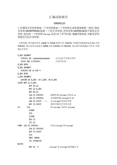
汇编试验报告090061101.所谓回文字符串是指一个字符串是指一个字符串正读和倒读都是一样的,例如字符串’ABCDEFFEDCBA’就是一个回文字符串,而字符串’ABCFDDCAB’就不是回文字符串.现在有一个字符串string,包含16个字节内容,请编写程序段,判断该字符串是否为回文字符串.分析思路:用串操作指令LODSB和STOSB将原字符STRING1串倒转存储到附加段ES中的STRING2,然后用串比较指令CMPSB比较STRING1和STRING2.若出现不相同输出字符Y,否则输出字符N.D_SEG SEGMENTSTRING1 DB 'AAAAAAAAAAAAAAAA' ;长为16字节的字符串COUNT EQU $-STRING1 ;字符串长度D_SEG ENDSE_SEG SEGMENTSTRING2 DB 16 DUP(?)E_SEG ENDSC_SEG SEGMENTASSUME DS:D_SEG, CS:C_SEG, ES:E_SEGSTART:MOV AX,D_SEGMOV DS,AXMOV AX,E_SEGMOV ES,AXLEA SI,STRING1 ;源操作数string1首址给siLEA DI,STRING2 ;目的操作数string2给diADD DI,COUNT – 1 ;由string2的末尾开始MOV CX,COUNT ;循环次数为字符串长度LP: CLD ;将string1反转至string2LODSBSTDSTOSBDEC CXJNZ LPCOMP: LEA SI,STRING1 ;比较string1和string2LEA DI,STRING2MOV CX,COUNTCLDREPZ CMPSBJNZ NOTMATCHMATCH:MOV DL,'Y' ;string1和string2相同输出'Y'MOV AH,02HINT 21HJMP EXITNOTMATCH:MOV DL,'N' ;string1和string2不同输出'N'MOV AH,02HINT 21HJMP EXITEXIT: MOV AH,4CHINT 21HC_SEG ENDSEND START2.将ELEMS中的100个字节数据的位置颠倒过来(即第一个字节和第100个字节的内容交换,第二个字节和第99个字节的内容交换……).分析思路:为了方便程序只做了将6个字节颠倒过来.程序先将原ELEMS打印到屏幕上,颠倒后再将新ELEMS打印的屏幕上.颠倒采用的方法同题1,使用串操作指令LODSB和STOSB将原串颠倒,再用串传送MOVSB将串复制到原来的地方.D_SEG SEGMENTELEMS DB '12345' ,'!' ;6个字节长的字符串LEN EQU $-ELEMS ;字符串长度D_SEG ENDSE_SEG SEGMENTSTRING DB 200 DUP(?)E_SEG ENDSC_SEG SEGMENTASSUME DS:D_SEG, ES:E_SEG, CS:C_SEGSTART:MOV AX,D_SEGMOV DS,AXMOV AX,E_SEGMOV ES,AXCALL PRINT ;将ELEMS输出到显示器LEA SI,ELEMSLEA DI,STRINGADD DI,LEN - 1MOV CX,LENLP:CLD ;将ELEMS反向存到string中LODSBSTDSTOSBDEC CXJNZ LPCOPY:MOV AX,E_SEG ;将string中的复制到原来ELEMS的地方MOV DS,AXMOV AX,D_SEGMOV ES,AXLEA SI,STRINGLEA DI,ELEMSMOV CX,LEN ;重复次数为串长度REP MOVSB ;重复CALL PRINT ;将新ELEMS输出到显示器MOV AH,4CHINT 21HPRINT PROC NEAR ;打印程序,打印ELEMSLEA BX,ELEMSMOV BYTE PTR[BX+LEN],'$' ;串尾部加'$'LEA DX,ELEMSMOV AH,09H ;调用字符串输出INT 21HMOV DL,0AHMOV AH,02HINT 21HMOV DL,0DHMOV AH,02HINT 21HRETPRINT ENDPC_SEG ENDSEND START3.请编写完整程序在一个升序字节数组中查找数N,找到后将此数从数组中删除,并使得CF=0,没找到返回CF=1.数组的首地址和末地址为A_HEAD和A_END.分析思路:采用二分查找的办法.首先将要寻找的数N与数组第一个数和最后一个数比较,当小于第一个或大于最后一个置CF=1, 如果等于第一个或最后1个置CF=0,同时将A_HEAD加1或将A_END减1.如果都不符合,调用二分查找的递归程序.递归首先判断终止条件(A_HEAD等于A_END),符合则CF=0,跳出至EXIT;然后计算中间位地址mid= (head+end)/2,比较要找的数与mid的大小,3种情况:一.当N=mid,置CF=0,然后将后面的元素依次前移一位,最后A_END减1.二.当N>mid,将mid地址给A_HEAD,调用二分查找三.当N<mid,将mid地址给A_END,调用二分查找D_SEG SEGMENTA_HEAD DW $+2 ;定义A_HEADARRAY DB 1,2,3,4,5,6,7,8,9 ;定义的升序字节数组A_END DW $-1 ;定义A_ENDN EQU 5 ;定义要找的数MID DB ?D_SEG ENDSC_SEG SEGMENTASSUME DS:D_SEG,CS:C_SEGSTART:MOV AX,D_SEGMOV DS,AXMOV BL,BYTE PTR[A_HEAD]CMP BL,N ;比较N和head JE TERM1JA TERM2MOV BL,BYTE PTR[A_END]CMP BL,N ;比较N和end JE TERM3JB TERM4MOV DX,A_HEAD ;DX存放head的地址MOV AX,A_END ;AX存放end的地址JMP HALFTERM1:CLC ;N=HEAD;置CF=0INC A_HEAD ;A_HEAD 后移一位,即删除JMP EXITTERM2:STC ;N<HEAD;置CF=1JMP EXITTERM3:CLC ;N=END;置CF=0DEC A_END ;A_END 前移一位,即删除JMP EXITTERM4:STC ;N>END;置CF=1JMP EXITHALF: CMP AX,DXJZ FOURMOV BX,DXADD BX,AX ;A_HEAD和A_END 相加,head + endSHR BX,1 ;折半,BX存放mid的地址CMP BYTE PTR[BX],NJA ONE ; N<midJB TWO ; N>midJZ THREE ; N=midONE: MOV DX,BX ;用mid的地址替换head的地址CALL HALFTWO: MOV AX,BX ;用mid的地址替换end的地址CALL HALFTHREE:CLC ;置CF=0MOV CX,A_ENDSUB CX,BX ;循环次数LP:MOV AL,[BX+1] ;删除元素,将后面的元素前移一位MOV [BX],ALINC BXDEC CXLOOP LPDEC A_ENDJMP EXITFOUR: STC ;没找到相应的N;置CF=1JMP EXIT EXIT: MOV AH,4CH INT 21HC_SEG ENDSEND START。
东南⼤学⼗套数据结构试题与答案.docx 数据结构试卷(⼀)三、算(每6分,共24 分)1. 在如下数 A 中存了⼀个性表,表指 A [0].next,写出性表。
A01234567data605078903440next35720412.画出下的接矩和接表。
3.已知⼀个的点集 V 和集 E 分: V={1,2,3,4,5,6,7};E={(1,2)3,(1,3)5,(1,4)8,(2,5)10,(2,3)6,(3,4)15,(3,5)12,(3,6)9,(4,6)4,(4,7)20,(5,6)18,(6,7)25};⽤克斯卡算法得到最⼩⽣成,写出在最⼩⽣成中依次得到的各条。
4. 画出向⼩根堆中加⼊数据4, 2, 5, 8, 3,每加⼊⼀个数据后堆的化。
四、算法(每7 分,共 14 分)1. LinkList mynote(LinkList L){//L是不点的表的指if(L&&L->next){q=L; L=L- >next ; p=L;S1:while(p->next) p=p->next;S2:p->next=q;q->next=NULL;}return L;}回答下列:(1)明句 S1 的功能;(2)明句 S2 的功能;(3)表表⽰的性表( a1,a 2, ? ,a n), 写出算法⾏后的返回所表⽰的性表。
2. void ABC(BTNode * BT){if BT {ABC (BT->left);ABC (BT->right);cout<data<<' ';}}算法的功能是:五、算法填空(共8 分)⼆叉搜索的找——算法:bool Find(BTreeNode* BST,ElemType& item){if (BST==NULL)return false; //查找失败else {if (item==BST->data){item=BST->data;//查找成功return ___________;}else if(itemdata)return Find(______________,item);else return Find(_______________,item);}//if}六、编写算法(共8 分)统计出单链表HL 中结点的值等于给定值X 的结点数。
Computer Organization and ArchitectureCOURSE DESIGNNAMESTUDENT NUMBERCOURSEComputer Organization and Architecture Course DesignPROJECTA Parallel Output Controller Basing On Verilog HDLSOFTWARE PLATFORMISE 14.1DATEMAR.17.20141. Purpose(1) To design and simulate a parallel output controller (POC) which acts an interface between system bus and printer.(2) The use of ISE software for design and simulation.2. Tasks(1) POC is one of the most common I/O modules, namely the parallel output controller. It plays the role of an interface between the computer system bus and the peripheral (such as a printer or other output devices).Figure 1 Printer ConnectionFigure shows the connecting of a printer to the system bus through the POC.(2) The communication between POC and the printer is controlled by a “handshake” protocol illustrated in Figure .Figure 2 The handshake-timing diagram between POC and the printer The handshaking process is described as follows: When the printer is ready to receive a character, it holds RDY=1.The POC must then hold a character at PD (parallel data) port and produce a pulse at the terminal TR (transfer request). Theprinter will change RDY to 0, take the character at PD and hold the RDY at 0 until the character has been printed (e.g. 5 or 10ms), then set RDY=1 again when it is ready to receive the next character. (Suppose the printer has only a one character “buffer” register, so that each character must be printed before the next character is sent).(3) The buffer register BR is used to hold a character that has been sent via the system bus while that the character is being transferred to the printer. The status register SR is used for two control functions: SR7serves as a ready flag for system bus transfers to BR (like the printer RDY signal for transfers from POC to the printer), and SR0 is used to enable or disable interrupt requests from POC. If SR0=1, then POC will interrupt when it is ready to receive a character (i.e., when SR7=1). If SR0=0, then POC will not interrupt. The other bits of SR are not used and empty.(4) The transfer of a character to POC via the system bus proceeds as follows.In polling mode, SR0 is always 0.The processor selects SR by accessing the relative address, then reads SR register, if SR7=1, the processor selects BR and writes a character into BR, then processor clears SR7 to indicate that the new character has been written into BR and not printed yet. When POC detects that SR7 is set to 0, POC then proceeds to start the handshaking operations with the printer. After sending character to printer, POC sets the SR7 to 1, which indicates POC is ready to receive another character from the processor. The transfer cycle can now repeat. During the handshaking operations between POC and printer, the processor continues to fetch and execute instructions. If it happens to read SR, it will find SR7=0 and hence will not attempt to send another character to the POC.In interrupt mode, SR0 is always 1.After sending character to printer, POC sets the SR7 to 1, since SR0=1, the interrupt request signal (IRQ) is set to 0, which indicate an effective interrupt signal to the processor. When the processor detects the effective IRQ signal, the processor directly selects BR and writes a character into BR, and then the processor sets the SR7 to 0, which indicates that the new character has been written into BR and not printed yet. When POC detects that SR7 is set to 0, POC then proceeds to start the handshaking operations with the printer. After sending character to printer, POC sets the SR7 to 1, which indicates POC is ready to receive another character from the processor. The transfer cycle can now repeat. During the handshaking operations between POC and printer, the processor does not try to access POC until it receives the interrupt request signal.3. The overall connection expressed in the top module formFigure 3 The overall connection expressed in the top module form In order to be easy to debug, some inside signals and registers are set as output signals. In fact, we just only need clk, clk2, reset, cs and PD to be outside signals.Table 1 The explication of the outside signals4. Design description of the simulation input waveformsAs is shown in table 1,4 simulation input signals are needed.(1)clk Clock of CPU and POC.(2)clk2Clock of Printer, faster than clk.(3)reset Reset when reset=0.(4)cs cs=0:polling mode; cs=1:interrupt mode.5. Simulation results(1)In polling mode, cs=0, SR0 is always 0.(2)In interrupt mode, cs=1, SR0 is always 1.6. Conclusions and DiscussionsPOC, parallel output controller, plays a role as an interface between CPU and the printer. As is shown above, the two simulation waves reveal that this design meets the requirements.In my design, all the codes are my original works. I have written the module Processor to help completing simulation, which need more codes and debugging to cooperate with the work of POC. Even there is already a schematic for the module Printer in the teaching material, I still have to do more work to finish this module because the software I use is ISE whose devices is different from those of Quartus II.The procedure of design helps me understand the working principle of interface. In the third term of Grade 2 did we learn something about computer interface in the course Microcomputer. And the course COA has referred to it, too. Here I use what I have learned to design this program and achieve a lot.In this program, I use the EDA software ISE and Verilog hardware language to design those three modules and Isim, which is a module of ISE, and VHDL language for simulation. As a result, I become more familiar with the use of hardware description language.Appendix------------------------------CPU------------------------------ module POC_CPU(output RW,output ADDR,output [7:0] POCDin,input reset,input CLK,input [7:0] POCDout,input IRQ);reg ADDR;reg [7:0] POCDin;reg RW;reg t1;reg t2;reg [7:0] n; //t为标记always@(posedge CLK)beginif(reset==0)begint1<=0;t2<=0;n<=8'b00000000;RW<=0;ADDR<=0;POCDin<=8'b00000000;endelse if(IRQ==0&&t2==0)//中断方式SR0=1,收到中断请求信号;beginADDR<=1;RW<=1;POCDin<=8'b00000101+n;t2<=1;endelse if(t2==1)beginADDR<=0;RW<=1;POCDin<=8'b00000001;t2<=0;n<=n+1;endelse if(RW==1&&POCDin==8'b00000001)begin RW<=0; end else//查询方式begin//ADDR<=0;RW<=0;if(RW==0&&POCDout==8'b10000000&&t1==0)//查询方式SR0=0,SR7=1;beginADDR<=1;RW<=1;POCDin<=8'b00000101+n;t1<=1;endif(POCDout==8'b10000000&&t1==1)//查询方式SR0=0,已完成数据传递,将把SR7置为0;beginADDR<=0;RW<=1;POCDin<=8'b00000000;t1<=0;n<=n+1;endif(RW==1&&POCDin==8'b00000000)begin RW<=0; end endendendmodule------------------------------POC------------------------------ module POC_POC(input ADDR,input [7:0] Din,input RW,input CLK,input reset,input cs,output IRQ,output TR,output [7:0] Dout,output [7:0] PD,output [7:0] SR,output [7:0] BR,input RDY);reg TR;reg [7:0] Dout;reg [7:0] PD;reg [7:0] BR;reg [7:0] SR;always@(posedge CLK)beginif(reset==0)beginIRQ<=1;TR<=0;Dout<=8'b00000000;PD<=8'b00000000;BR<=8'b00000000;SR<=8'b00000000;endelse if(cs==0)//查询方式beginif(ADDR==0&&RW==0)//读SR到CPUbeginif(SR[7]==0&&RDY==1&&TR==0)beginPD<=BR;TR<=1;Dout<=SR;endelse if(TR==1) begin TR<=0;SR[7]<=1;Dout<=SR; endelse begin Dout<=SR; endendif(ADDR==0&&RW==1)//写SR BR写入新数据后SR7被置为0 beginSR<=Din;end/*if(ADDR==1&&RW==0)//读BRbeginDout<=BR;end*/if(ADDR==1&&RW==1)//写BRbeginif(SR[7]==0&&RDY==1&&TR==0)beginBR<=Din;TR<=1;Dout<=8'b00000000;endelse if(TR==1) begin TR<=0;SR[7]<=1;BR<=Din;Dout<=8'b00000000; end else begin BR<=Din;Dout<=8'b00000000; endendendelse if(cs==1)//中断方式beginif(SR[0]==0)begin SR<=8'b00000001; endelse if(ADDR==0&&RW==0) //读SRbeginif(SR[7]==0&&RDY==1&&TR==0)beginPD<=BR;TR<=1;IRQ<=1;Dout<=SR;endelse if(TR==1) begin TR<=0;IRQ<=0;SR[7]<=1;Dout<=SR; endelse begin Dout<=SR;IRQ<=1; endendelse if(ADDR==0&&RW==1) //写SR BR写入新数据后SR7被置为0 beginSR<=Din;end/*if(ADDR==1&&RW==0) //读BRbeginDout<=BR;end*/else if(ADDR==1&&RW==1) //写BR 此时SR7不可能为0beginif(SR[7]==0&&RDY==1&&TR==0)beginBR<=Din;PD<=BR;TR<=1;IRQ<=1;Dout<=8'b00000001;endelse if(TR==1)beginTR<=0;IRQ<=0;SR[7]<=1;BR<=Din;Dout<=8'b00000001;end//else if(IRQ==0) begin IRQ<=1; endelse begin BR<=Din;IRQ<=1;Dout<=8'b00000001; endendendendendmodule------------------------------Printer------------------------------。