
Cool MOS? Power Transistor
Feature
? New revolutionary high voltage technology ? Worldwide best R DS(on) in TO 220? Ultra low gate charge ? Periodic avalanche rated ? Extreme d v /d t rated
? Ultra low effective capacitances
Product Summary 650V R DS(on)0.19?I D
20
A
V DS @ T jmax P-TO220-3-1
Marking 20N60C220N60C220N60C2
Type Package Ordering Code
SPP20N60C2P-TO220-3-1Q67040-S4320SPB20N60C2P-TO263-3-2
Q67040-S4322
SPA20N60C2
P-TO220-3-31Q67040-S4333
Maximum Ratings Parameter
Symbol Value Unit
SPA
Continuous drain current
T C = 25 °C T C = 100 °C
I D
2013
201)131)A
Pulsed drain current, t p limited by T jmax I D puls 4040A Avalanche energy, single pulse
I D =10A, V DD =50V
E AS 690690mJ
Avalanche energy, repetitive t AR limited by T jmax 2)
I D =20A, V DD =50V
E AR 11Avalanche current, repetitive t AR limited by T jmax I AR
2020A Reverse diode d v /d t
I S = 20 A, V DS < V DD , d i /d t =100A/μs, T jmax =150°C
d v /d t 66V/ns Gat
e source voltage
V GS ±20±20V Gate source voltage AC (f >1Hz)V GS ±30
±30
Power dissipation, T C = 25°C
P tot
20834.5
W
SPP_B
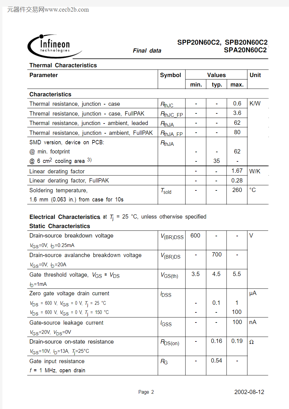
Thermal Characteristics
Parameter Symbol Values Unit
min.typ.max. Characteristics
Thermal resistance, junction - case R thJC --0.6K/W Thremal resistance, junction - case, FullPAK R thJC_FP-- 3.6 Thermal resistance, junction - ambient, leaded R thJA--62 Thermal resistance, junction - ambient, FullPAK R thJA_FP--80
SMD version, device on PCB: @ min. footprint
@ 6 cm2 cooling area 3)R thJA
-
-
-
35
62
-
Linear derating factor-- 1.67W/K Linear derating factor, FullPAK--0.28 Soldering temperature,
1.6 mm (0.063 in.) from case for 10s
T sold --260°C
Electrical Characteristics, at T j = 25 °C, unless otherwise specified
Static Characteristics
Drain-source breakdown voltage
V GS=0V, I D=0.25mA
V(BR)DSS600--V Drain-source avalanche breakdown voltage
V GS=0V, I D=20A
V(BR)DS-700-
Gate threshold voltage, V GS = V DS
I D=1mA
V GS(th) 3.5 4.5 5.5
Zero gate voltage drain current V DS = 600 V, V GS = 0 V, T j = 25 °C V DS = 600 V, V GS = 0 V, T j = 150 °C I DSS
-
-
0.1
-
1
100
μA
Gate-source leakage current
V GS=20V, V DS=0V
I GSS--100nA Drain-source on-state resistance
V GS=10V, I D=13A, T j=25°C
R DS(on)-0.160.19?
Gate input resistance
f = 1 MHz, open drain
R G-0.54-
Electrical Characteristics
Parameter Symbol Conditions Values Unit
min.typ.max. Characteristics
Transconductance g fs V DS≥2*I D*R DS(on)max,
I D=13A
-12-S
Input capacitance C iss V GS=0V, V DS=25V,
f=1MHz -3000-pF
Output capacitance C oss-1170-Reverse transfer capacitance C rss-28-
Effective output capacitance,4) energy related C o(er)V GS=0V,
V DS=0V to 480V
-83-
Effective output capacitance,5)
time related
C o(tr)-160-
Turn-on delay time t d(on)V DD=380V, V GS=0/13V,
I D=20A,
R G=3.6?, T j=125°C -21-ns
Rise time t r-51-
Turn-off delay time t d(off)-5684
Fall time t f-69
Gate Charge Characteristics
Gate to source charge Q gs V DD=350V, I D=20A-21-nC Gate to drain charge Q gd-46-
Gate charge total Q g V DD=350V, I D=20A,
V GS=0 to 10V
-79103
Gate plateau voltage V(plateau)V DD=350V, I D=20A-8-V
1Limited only by maximum temperature
2Repetitve avalanche causes additional power losses that can be calculated as P
AV
=E AR*f.
3Device on 40mm*40mm*1.5mm epoxy PCB FR4 with 6cm2 (one layer, 70 μm thick) copper area for drain connection. PCB is vertical without blown air.
4C
o(er)
is a fixed capacitance that gives the same stored energy as C oss while V DS is rising from 0 to 80% V DSS.
5C
o(tr)
is a fixed capacitance that gives the same charging time as C oss while V DS is rising from 0 to 80% V DSS.
Electrical Characteristics
Parameter Symbol Conditions Values Unit
min.typ.max. Characteristics
Inverse diode continuous
forward current
I S T C=25°C--20A
Inverse diode direct current,
pulsed
I SM--40 Inverse diode forward voltage V SD V GS=0V, I F=I S-1 1.2V
Reverse recovery time t rr V R=350V, I F=I S ,
d i F/d t=100A/μs -6101040ns
Reverse recovery charge Q rr-12-μC Peak reverse recovery current I rrm-48-A Peak rate of fall of reverse
recovery current
di rr/dt T j=25°C-1500-A/μs
1 Power dissipation P tot = f (T C)
P
t
o
t
2 Power dissiaption FullPAK
P tot = f (T C)
P
t
o
t
3 Safe operating area
I D = f ( V DS )
parameter : D
= 0 , T C=25°C
3
I
D
4 Safe operating area FullPAK
I D = f (V DS)
parameter: D = 0,
T C = 25°C
3
I
D
5 Transient thermal impedance Z thJC = f (t p )parameter: D = t p /T
10 10 10 10 10 K/W Z t h J C
6 Transient thermal impedance FullPAK Z thJC = f (t p )parameter: D = t p /t
1
10 10 10 10 10 K/W
Z t h J C
7 Typ. output characteristic I D
= f (V DS ); T j =25°C parameter: t p = 10 μs, V GS
I
D
8 Typ. output characteristic I D = f (V DS ); T j =150°C parameter:
t p = 10 μs, V GS
I D
9 Typ. drain-source on resistance R DS(on)=f(I D)
parameter: T j=150°C, V GS
R
D
S
(
o
n
)
10 Drain-source on-state resistance
R DS(on) =
f (T j)
parameter : I D = 13 A, V GS = 10 V
SPP20N60C2
R
D
S
(
o
n
)
11 Typ. transfer characteristics
I D= f ( V GS );
V DS≥ 2 x I D x R DS(on)max
parameter: t p = 10 μs
I
D
12 Typ. gate charge
V GS= f (Q Gate)
parameter: I = 20 A pulsed
V
G
S
13 Forward characteristics of body diode
I F = f (V SD)
parameter: T
, t p = 10 μs
I
F
14 Typ. switching time
t = f (I D), inductive load, T j=125°C
par.: V DS=380V, V GS=0/+13V, R G=3.6?
15 Typ. switching time
t = f (R G), inductive load, T j=125°C
par.: V DS=380V, V GS=0/+13V, I D=20A
10
10
10
10
ns
t
16 Typ. switching losses1)
E =
f (I D), inductive load, T j=125°C
par.: V DS=380V, V GS=0/+13V, R G=3.6?
mWs
E
17 Typ. switching losses1)
E = f(R G), inductive load, T j=125°C par.: V DS=380V, V GS=0/+13V,I D=20A
mWs
E
18 Avalanche SOA
I AR = f (
t AR)
par.: T j≤ 150 °C
4
I
A
R
19 Avalanche energy
E AS = f (T
j)
par.: I D = 10 A, V DD = 50 V
mJ
750
E
A
S
20 Drain-source breakdown voltage
V(BR)DSS = f (T j)
SPP20N60C2
V
(
B
R
)
D
S
S
21 Avalanche power losses P AR = f (f )
parameter: E AR =1mJ
6
W
P A R
22 Typ. capacitances C = f (V DS )
parameter: V GS =0V, f =1 MHz
23 Typ. C oss stored energy E oss =f (V
DS )
μJ
14
E o s s
Definition of diodes switching characteristics
P-TO-220-3-1
All metal surfaces tin plated, except area of cut. Metal surface min. x=7.25, y=12.3
P-TO-263-3-1 (D2-PAK)
1)
Typical
All metal surfaces: tin plated, except area of cut.
Metal surface min. x=7.25, y=6.9
P-TO-220-3-31 (FullPAK)
Please refer to mounting instructions (application note AN-TO220-3-31-01)
Published by
Infineon Technologies AG,
Bereichs Kommunikation
St.-Martin-Strasse 53,
D-81541 München
? Infineon Technologies AG 1999
All Rights Reserved.
Attention please!
The information herein is given to describe certain components and shall not be considered as warranted characteristics.
Terms of delivery and rights to technical change reserved.
We hereby disclaim any and all warranties, including but not limited to warranties of non-infringement, regarding circuits, descriptions and charts stated herein.
Infineon Technologies is an approved CECC manufacturer.
Information
For further information on technology, delivery terms and conditions and prices please contact your nearest Infineon Technologies Office in Germany or our Infineon Technologies Reprensatives worldwide (see address list). Warnings
Due to technical requirements components may contain dangerous substances.
For information on the types in question please contact your nearest Infineon Technologies Office.
Infineon Technologies Components may only be used in life-support devices or systems with the express
written approval of Infineon Technologies, if a failure of such components can reasonably be expected to
cause the failure of that life-support device or system, or to affect the safety or effectiveness of that device
or system Life support devices or systems are intended to be implanted in the human body, or to support
and/or maintain and sustain and/or protect human life. If they fail, it is reasonable to assume that the health
of the user or other persons may be endangered.