Blackfin内核体系结构(2008年11月)blackfin_core_architecture_overview_transcript
- 格式:pdf
- 大小:140.18 KB
- 文档页数:21
Blackfin561 VS TMS320DM642 全面比较德州仪器公司(Texas Instruments以下简称TI公司)和美国模拟器件公司(Analog Devices以下简称ADI公司),作为全球领先的高性能DSP供应商,它们几乎占据了全球DSP市场全部分额。
TMS320DM642(以下简称DM462)是TI公司近来发布的新一代多媒体处理器,它基于其第二代高性能的 VelociTI VLIW结构,适用于多种数字媒体应用,它的时钟频率为600MHz,指令速度高达4800MIPS。
而ADSP-BF561(以下简称BF561)处理器是ADI公司推出的Blackfin 系列中的高性能产品,主要针对于多媒体和通信方面的各种应用。
BF561的核心由两枚独立的Blackfin 处理器组成。
它集成了一套通用的数字图像处理外围设备,为数字图像处理和多媒体应用创建了一个完整的系统级片上解决方案。
下面我们将对TI公司的 TMS320DM642与ADI公司的Blackfin561做一些简要介绍和比较。
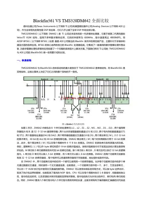
一、体系结构TMS320DM642与Blackfin561的体系结构的最大差别在于TMS320DM642是单核结构、而Blackfin561是双核结构,这就从整体上决定了它们之间的整个架构的不一致性。
图1 DM642的内核结构如图1所示,DM642内核包含8 个并行的处理单元(.L1,.L2,.S1,.S2,M1,.M2,.D1,.D2),两个通用寄存器组(A和B,各32 个32-bit通用寄存器),两个从内存读取数据的通道(LD1和LD2),两个写内存的数据通道(ST1和ST2),两个数据地址通道(DA1和DA2),两个寄存器组数据交叉通道(1X和2X),两个乘法单元(M)、六个32-bit 的算术单元、40-bit的ALU和40-bit的桶型移位器。
DM642乘法单元(M)每个时钟周期执行两个16-bit的乘法,此外,每个乘法单元(M)可以在每个周期内作4 个8 bit 的乘法。
深入了解Windows Server 2008 内核变化内存管理和SMB 2.0 NTFS 自修复功能、Windows 硬件错误报告体系和驱动程序验证程序I/O 完成端口、线程池和NUMA 的可伸缩性Hyper-V 虚拟化Windows Server 2008 是最新版本的Microsoft 服务器平台,它包含许多系统级更改,这些更改涉及操作系统的所有功能领域:从内存管理到线程调度,从网络连接到安全(这里只列出了少数几个)。
由于Windows Server®2008 和Windows Vista®SP1 的内核相同,因此它包含许多我曾经在之前的《TechNet 杂志》文章:“深入了解Windows Vista 内核”第1-3 部分(2007 年2 月、3 月和4 月)和“深入了解Windows Vista 用户帐户控制”(2007 年6 月)中介绍过的增强功能。
只有其中的少数功能仅特定于客户端且并未包含在Windows Server 2008 中,如SuperFetch、ReadyBoost、ReadyDrive、Ready Boot 和多媒体类计划程序服务(MMCSS)。
因此,我将不再重复介绍Windows Vista 中已介绍过且Windows Server 2008 中同样包含的重要内核变化,如I/O 优先级排列、新的引导体系结构BitLocker TM、代码完整性和强制完整性级别。
我将重点介绍之前这些文章中未涉及到的关键变化,包括与可靠性、性能、可伸缩性以及新的Microsoft 管理程序计算机虚拟化技术Hyper-V TM相关的变化。
同样,与之前的文章一样,本文的范围仅限于操作系统内核Ntoskrnl.exe 以及与其紧密关联的系统组件的变化。
例如,本文不会介绍安装(WIM 或Windows®映像格式和基于组件的服务)、管理(组策略和Active Directory®改进)、常规诊断和监控(Windows 诊断基础结构)、核心网络(新的防火墙和TCP/IP 实现)、Server Core 或服务器角色的变化。
linux内核原理Linux内核是一个开放源代码的操作系统内核,它是由林纳斯·托瓦兹(Linus Torvalds)在上世纪90年代初开发而来。
Linux内核的设计遵循了Unix操作系统的许多原则,并且具有高度的可移植性、可扩展性和稳定性。
它是目前世界上被广泛使用的最流行的操作系统内核之一。
要了解Linux内核的工作原理,首先要明白内核的主要功能是什么。
内核的主要任务是管理计算机硬件资源的分配和控制,为上层应用程序提供操作系统服务和功能。
它是操作系统的核心部分,负责处理硬件设备的输入输出、内存管理、进程调度、文件系统等基本功能。
Linux内核的设计基于模块化的原则,它由多个不同的模块组成,每个模块负责不同的功能。
这种模块化的设计使得Linux内核具有灵活和可定制的特性,允许用户根据自己的需求选择加载或卸载不同的功能模块。
内核的开发过程通过一个分布式的方式进行,每个开发者都可以独立地开发和贡献代码。
这种开发模式使得内核的开发过程高效且灵活,有助于快速解决问题和推出新的功能。
同时,内核的开放源代码使得任何人都可以查看和修改内核的代码,从而更好地适应不同的硬件平台或应用需求。
Linux内核的主要组成部分包括进程管理、内存管理、文件系统、设备驱动等功能模块。
进程管理模块负责管理系统中的各个进程,包括进程的创建、终止、调度等。
内存管理模块负责管理系统的内存资源,包括内存的分配和回收、虚拟内存管理等。
文件系统模块负责管理系统中的文件和目录,包括文件的读写和权限控制等。
设备驱动模块负责管理系统中的硬件设备,包括设备的初始化、中断处理等。
在Linux内核的运行过程中,不同的模块之间通过系统调用和中断机制进行通信和协调。
系统调用是用户程序与内核之间的接口,用户程序可以通过系统调用请求内核提供各种操作系统服务,如文件读写、进程创建等。
中断是外部设备向内核发出的一种异步请求,例如硬盘IO完成、时钟中断等。
内核需要及时响应这些中断请求,并根据需要做出相应的操作。
linux系统逻辑构架-回复[Linux系统逻辑构架]是指Linux操作系统的内部结构和组织。
Linux系统的逻辑构架是一个多层次的体系结构,它由多个模块和组件组成,每个模块和组件有自己的功能和责任。
1. 内核层(Kernel Layer)内核层是Linux系统的核心部分,负责提供最基本的操作系统功能。
它包括底层设备驱动程序、进程管理、内存管理、文件系统和网络协议栈等模块。
内核层是整个系统的基础,它为上层应用程序提供了访问硬件资源和系统服务的接口。
2. 系统调用层(System Call Layer)系统调用层位于用户空间和内核空间之间,提供了用户程序与内核之间的通信接口。
用户程序通过系统调用,向内核发起请求以获取各种操作系统服务,如文件操作、进程管理和网络通信等。
系统调用层实现了一组标准的接口,供用户程序使用,隐藏了底层硬件和内核细节。
3. 库函数层(Library Layer)库函数层是构建在系统调用层之上的软件层,为应用程序提供了一系列常用功能的函数库。
常见的库包括标准C库(libc)和其他语言特定的库,如Python的标准库(stdlib)。
库函数层封装了底层系统调用和底层数据结构,提供了更高级的函数接口和数据结构,简化了应用程序的开发和维护。
4. 工具层(Utility Layer)工具层是Linux系统中一些常用的命令行工具和实用程序,如shell环境、文本编辑器和文件管理器等。
这些工具和实用程序通常位于/bin、/usr/bin 和/usr/local/bin等目录下,供用户直接使用。
工具层提供了一种交互式的操作方式,用户可以通过命令行输入命令,执行各种系统操作和管理任务。
5. 图形用户界面层(Graphical User Interface Layer)图形用户界面层是Linux系统的上层部分,为用户提供了一种图形化的操作界面。
它包括窗口管理器、桌面环境和应用程序等。
常见的图形用户界面有Gnome、KDE和XFCE等。

linux分层设计体系结构Linux是一种开源的操作系统,其设计采用了分层的体系结构。
这种设计使得Linux具有高度的灵活性和可扩展性,同时也方便了系统的维护和管理。
本文将详细介绍Linux的分层设计体系结构。
在Linux的分层设计中,最底层是硬件层。
硬件层包括计算机的各种硬件设备,如处理器、内存、硬盘、网络接口等。
Linux通过设备驱动程序来管理和控制这些硬件设备,使其能够与操作系统进行交互。
在硬件层之上是内核层。
内核是操作系统的核心,负责管理系统的资源和提供各种系统服务。
Linux的内核是一个单独的模块,可以独立于其他软件进行开发和维护。
内核提供了各种系统调用接口,以及对进程、文件系统、网络和设备的管理和控制功能。
在内核层之上是库层。
库是一组共享的代码和函数,可以为应用程序提供常用的功能和服务。
Linux提供了许多不同的库,如C库、数学库、网络库等。
这些库可以被开发人员用来开发应用程序,提高开发效率和代码复用性。
在库层之上是应用层。
应用层包括各种应用程序和工具,如文本编辑器、图形界面、网络浏览器等。
这些应用程序可以通过系统调用接口与内核进行交互,并利用库提供的功能来实现各种任务和操作。
除了以上四个层次外,Linux还有其他一些重要的组件和模块。
例如,系统初始化和启动过程中,会加载引导程序和初始化程序;文件系统是用来组织和管理文件和目录的;网络协议栈是用来实现网络通信的;系统服务是用来提供各种系统功能和服务的。
这些组件和模块与其他层次之间相互关联,共同构成了Linux的完整体系结构。
Linux的分层设计体系结构具有许多优点。
首先,分层设计使得系统的各个组件和模块之间相互独立,可以分别进行开发、测试和维护,提高了开发和维护效率。
其次,分层设计使得系统的各个层次之间的接口清晰明确,方便了系统的扩展和升级。
此外,分层设计还提高了系统的稳定性和可靠性,一旦某个层次出现问题,不会对其他层次造成影响。
Linux的分层设计体系结构是一种高效、灵活和可扩展的设计方式。
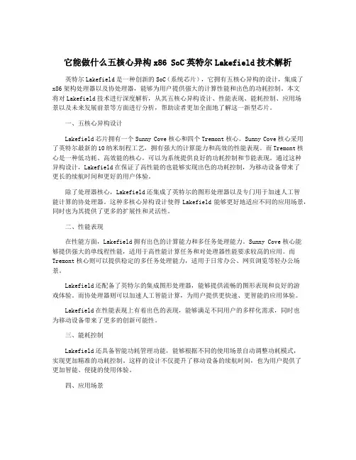
它能做什么五核心异构x86 SoC英特尔Lakefield技术解析英特尔Lakefield是一种创新的SoC(系统芯片),它拥有五核心异构的设计,集成了x86架构处理器以及协处理器,能够为用户提供强大的计算性能和出色的功耗控制。
本文将对Lakefield技术进行深度解析,从其五核心异构设计、性能表现、能耗控制、应用场景以及未来发展前景等方面进行分析,帮助读者更加全面地了解这一新型芯片。
一、五核心异构设计Lakefield芯片拥有一个Sunny Cove核心和四个Tremont核心。
Sunny Cove核心采用了英特尔最新的10纳米制程工艺,拥有强大的计算能力和高效的性能表现。
而Tremont核心是一种低功耗、高效能的核心,可以为系统提供良好的功耗控制和节能表现。
通过这种异构设计,Lakefield在保证了高性能的也能够实现出色的功耗控制,为移动设备带来了更长的续航时间和更好的用户体验。
除了处理器核心,Lakefield还集成了英特尔的图形处理器以及专门用于加速人工智能计算的协处理器。
这种多核心异构设计使得Lakefield能够更好地适应不同的应用场景,同时也为其提供了更多的扩展性和灵活性。
二、性能表现在性能方面,Lakefield拥有出色的计算能力和多任务处理能力。
Sunny Cove核心能够提供强大的单线程性能,适用于高性能计算任务和对处理器性能要求较高的应用。
而Tremont核心则可以提供稳定的多任务处理能力,适用于日常办公、网页浏览等轻办公场景。
Lakefield还配备了英特尔的集成图形处理器,能够提供流畅的图形表现和良好的游戏体验。
而协处理器则可以加速人工智能计算,为用户提供更快速、更智能的应用体验。
Lakefield在性能表现上有着出色的表现,能够满足不同用户的多样化需求,同时也为移动设备带来了更多的创新可能性。
三、能耗控制Lakefield还具备智能功耗管理功能,能够根据不同的使用场景自动调整功耗模式,实现更加精准的功耗控制。

操作系统内核的基础知识和编程技巧操作系统内核的基础知识和编程技巧随着计算机技术的不断发展,操作系统(Operating System,简称OS)也得到了极大的发展。
计算机所运行的应用程序必须借助于操作系统来完成各种各样的任务,而操作系统内核则是操作系统的核心。
因此,了解操作系统内核的基础知识和编程技巧是每个计算机专业人员必备的技能之一。
什么是操作系统内核?操作系统内核是操作系统的核心组件,也是操作系统最为关键的部分。
它是运行在控制台上的程序,控制着计算机系统的硬件部件以及应用程序。
操作系统内核负责管理系统的输入输出,调度进程和线程,内存管理,文件系统管理等重要任务。
操作系统内核的结构操作系统内核通常由若干个模块组成,每个模块负责不同的任务。
内核的结构可以通过分层的方式来描述。
在分层结构中,每个层级的组件都为上一层提供服务,并且它们接收下一层组件的请求。
系统调用操作系统内核的核心功能之一就是系统调用(System Call),也可以叫做内核调用(Kernel Call)。
一个系统调用是应用程序通过操作系统内核来访问系统资源的一种标准方式。
系统调用常见的应用有开启一个文件、读取一个文件或打开一个网络连接等。
系统调用过程可以总结为以下几个步骤:1.用户程序通过应用程序编程接口(API)调用操作系统内核函数。
2.操作系统内核函数接收请求并验证是否合法。
3.内核函数执行相应的系统操作。
4.操作完成后,内核函数返回结果给用户程序。
系统调用对于操作系统内核的稳定性非常重要。
因此,内核调用的执行必须获得足够的控制和保护。
此外,编写一个内核调用需要非常小心,因为它可以直接影响到整个系统的性能。
进程调度进程调度是操作系统内核的另一个核心功能。
进程调度是指操作系统如何安排进程使用CPU的时间,使多个进程在CPU上执行,从而实现进程间的并发执行。
在多任务环境下,操作系统可以在各个进程之间进行调度,以便它们充分利用CPU资源。
uCLinux在Blackfin处理器上的应用
佚名
【期刊名称】《《世界电子元器件》》
【年(卷),期】2005(000)001
【摘要】作为信号处理芯片的主要供应商之一,Analog Devices公司(ADI)一直致力发展高性价比的产品.Blackfin系列处理器是ADI公司的最新的基于微信号体系结构的嵌入式处理器,具有高性能和低功耗等特点.利用内核中的两个MAC运算单元,750MHz的BF533处理器每秒可完成1500M的MAC,而双核的BF561处理器每秒可完成3000M的MAC.
【总页数】7页(P92-98)
【正文语种】中文
【中图分类】TN929.53
【相关文献】
1.智能型视频监控系统及其在Blackfin处理器上的应用 [J], 魏宏伟;张铁虎
2.ADI公司的最新Blackfin处理器系列产品对汽车应用的系统性能和嵌入安全技术再创新高——Blackfin处理器解决了多媒体、网络汽车和工业应用的电子设计难题 [J], ADI公司
3.μClinux 在 Blackfin561 处理器上的应用 [J], 魏坤;武富春
4.uCLinux在Blackfin处理器上的应用 [J], Analog Devices公司
5.ADI公司发布最新适合汽车应用基于闪存的Blackfin处理器——XM卫星广播公司、VoiceBox Technologies公司和沃尔沃公司采用Blackfin处理器用于需要附加闪存的复杂汽车设计 [J],
因版权原因,仅展示原文概要,查看原文内容请购买。

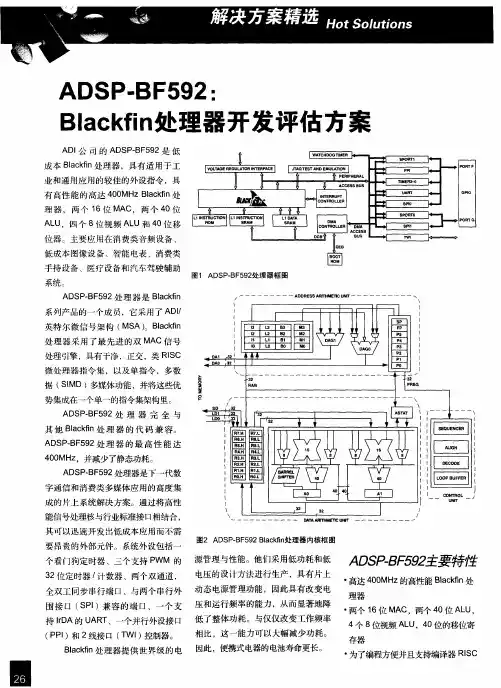
如何实现高性能的DSP处理(下)相关阅读:Blackfin 的存储器体系为了使第一部分的研究越发透亮化,现在对Blackfin的存储器结构加以描述。
Blackfin的存储系统也提供一些“按钮”,以便开发者可以将其打开从而提高系统性能。
我们将要研究怎样才干最充分地利用这些“按钮”。
Blackfin有三级存储结构。
第1级(L1)存储器离内核最近,其工作速率为处理器的内核时钟频率(Blackfin典型频率为600MHz),并为命令和数据提供单周期存取操作。
典型的L1存储器可存储几十KB,还可按照SRAM 或 cache举行调配。
芯片內部的第2级(L2)存储器位于芯片内部但离处理器内核较远。
对该存储器中命令和数据的拜访可能要用几个周期。
芯片內部L2级存储器容量普通为几百KB,典型的有128KB和256KB。
芯片外部L2级存储器位于芯片外部,因此所提供的存取操作也最为耗时。
它工作频率为系统时钟,该时钟频率通常为133MHz。
但是芯片外部L2级存储器容量往往很大,典型的有几百兆字节。
中断处理大多数系统都含有中断,因此适当地处理中断十分重要。
普通需要了解两个问题:每个中断服务程序耗费多少时光,以及一个中断服务程序是否正在阻挡其他关键代码的执行。
假如系统支持中断嵌套,例如能够中断一个正在执行的低优先权的中断,就还有须要知道如何实现最好的嵌套中断。
在Blackfin中,假如一个中断正在执行,其他中断默认是关闭的。
然而,开发者可以通过将正在运行的中断服务子程序(ISR)的返回地址存入堆栈中来激活一个更高优先权的中断(即嵌套中断)。
中断嵌套保证了优先权高的中断不会被优先权低的中断阻挡。
为了使这一过程越发容易,公司提供了一个“回调管理器”,它能保证中断被的准时响应,第1页共4页。
ADSP处理器PPI接口和DMAADSP处理器的并行外设接口PPIADSP处理器的DMAADSP处理器的并行外设接口PPIPPI概述PPI接口是ADSP‐BF533新推出的一种外部接口,全称为并行外围接口,是数据高速传输专用的半双工双向通道。
该接口包括16位接口是数据高速传输专用的半双工双向通道该接口包括的数据传输线、3个同步信号和一个时钟信号。
与其它DSP通用并行数据的区别在于行数据口的区别在于:不需要地址线配合,直接与DMA通道整合,读写数据时自动地址增减。
由于去掉了地址线,减少了电路设计时地址线布线的面积。
而且由于传输道而且,由于PPI接口具有专门的DMA传输道,DSP内核可以在数据传输的同时进行高速数据处理,大大提高了DSP的效率。
具有帧同步信号,不产生读信号和写信号。
其它DSP每读写一个数据都会产生一个读写信号,而PPI提供的3个同步信号均是帧同步信号,每帧数据传输前产生一个高电平的同步信号。
这些同步信号配灵活,可根据设计要求配为个或者个同步信号信号配置灵活可根据设计要求配置为0、13个同步信号。
时钟信号配置灵活。
时钟作为输入信号,既可直接由外部时钟源提供,也可以由DSP自身系统时钟分频输出后再作为输入时钟,最高频率为系统时钟频率的一半。
该时钟信号决定高频率为系统时钟频率的半。
该时钟信号决定PPI传输的速度,这就增强了接口速度的灵活性。
其它DSP的并行数据接口也具有DMA通道,但是DMA速度一般不可调节,如果有严格的速度和时序要求时必须外部接上等缓冲设备对于低功耗和体积受序要求时,必须外部接上FIFO等缓冲设备,对于低功耗和体积受限的掌上设备而言是很不利的。
由于PPI口具有独立的时钟和同步信号,该接口可以直接连接AD、DA、视频编解码器以及其它通用外设并保证时钟严格同步外设,并保证时钟严格同步。
数据传输宽度可以灵活设定,可设置为8位、10位~16位等8种数据宽度。
PPI的16位数据线中高12位与ADSP‐BF533的PF4~PF15(Program flag,可编程标志)复用,低4位是专用数据线PPI0~可编程标志复用低PPI3。
Blackfin 处理器优化的嵌入式系统设计资源简化汇聚式处理器应用当今的嵌入式应用已经无处不在,全球每年生产数十亿颗微处理器,其中大部分被广泛应用于各类嵌入式系统,从消费电子、通信终端及系统设备、工业控制、汽车电子系统到航空航天,无处不能看到嵌入式应用的身影。
在硬件平台方面微控制器以及数字信号处理器(DSP)产品无论从品牌、成本、功能特性方面选择数以千计,您完全可以针对您的目标应用对成本、处理能力、功耗要求、集成度、开发周期、技术难度等具体要求,精心选择出最具综合优势的硬件核心平台。
而在嵌入式操作系统方面,您同样不再会有桌面应用中几乎无可选择的尴尬,无论是开放源代码的Linux阵营的各种商业版本或免费版本,还是WinCE、vxWorks等“重量级”平台,抑或针对特定应用优化的如Windows Mobile、Symbian、Android 等,您同样可以为您的目标应用选择一款最佳的操作系统软件平台。
嵌入式系统设计过程是软硬件联合协同开发的过程,在进行软硬件平台选择评估时,单纯地离开硬件去评估操作系统或离开操作系统评估硬件平台都有失偏颇,特别是对于很多非通用处理器来说尤其如此。
当前很多嵌入式硬件平台都提供了针对目标应用优化的操作系统及软件模块资源,一些商业化的操作系统也针对主流的硬件平台进行了优化设计,提供第三方优化操作系统版本,这些资源对于嵌入式系统设计来说具有重要的意义。
本文将介绍一种独特的嵌入式平台核心处理器——汇聚式处理器Blackfin以及其主流的配套操作系统及相关资源。
基于Blackfin构建独特的嵌入式平台汇聚式处理器Blackfin 基于由 ADI 和 Intel 公司联合开发的微信号架构(MSA),它将一个 32 位 RISC 型指令集和双 16 位乘法累加(MAC)信号处理功能与通用型微控制器所具有的易用性组合在一起。
A © 2007 Analog Devices, Inc. Page 1 of 21B lackfin O nline L earning & D evelopmentPresentation Title: Blackfin Processor Core Architecture OverviewPresenter: George KadziolkaChapter 1: IntroductionSubchapter 1a: Module OverviewSubchapter 1b: Blackfin Family OverviewSubchapter 1c: Embedded Media ApplicationsChapter 2: The Blackfin CoreSubchapter 2a: Core OverviewSubchapter 2b: Arithmetic UnitSubchapter 2c: Addressing UnitSubchapter 2d: Circular BufferingSubchapter 2e: SequencerSubchapter 2f: Event HandlingSubchapter 2g : FIR Filter exampleChapter 3: The Blackfin Bus and Memory ArchitectureSubchapter 3a: OverviewSubchapter 3b: Bus StructureSubchapter 3c: Configurable MemorySubchapter 3d: Cache and Memory ManagementChapter 4: Additional Blackfin Core FeaturesSubchapter 4a: DMASubchapter 4b: Dynamic Power ManagementSubchapter 4c: Blackfin Hardware Debug SupportChapter 5: ConclusionSubchapter 5a: SummarySubchapter 5b: ResourcesChapter 1: INTRODUCTIONSubchapter 1a: Module Overviewa© 2007 Analog Devices, Inc. Page 2 of 21 B lackfin O nline L earning & D evelopment Hello, this presentation is entitled The Blackfin Core Architecture Overview. My name is George Kadziolka. I’m the President of Kaztek Systems. I’ve been personally providing the training on the variousAnalog Devices architectures since 2000.This module will introduce the Blackfin family which includes the Blackfin processors, tools and other development support that’s available. Then we’re going to get into the Blackfin Core Architecture and tell you a little bit about what’s going on under the hood.The Blackfin family will be the first stop, we’re going to talk about the Blackfin processor, some of theorigins, the tools that are available, then we’ll get into the Blackfin core, talk about the arithmetic operation, data fetching, program flow control with the sequencer. We’ll get into the Blackfin bus architecture and hierarchal memory structure. We’ll talk about caching when we get to the memory management section.Additional Blackfin core features will also be touched on including DMA, Power Management as well as some of the hardware debug support that’s available.Subchapter 1b: Blackfin Family OverviewThe Blackfin family consists of a broad range of Blackfin processors to suit a number of differentapplications. There’s also a wide variety of software development tools available, Analog Devices for instance provides VisualDSP++ and supports a uCLinux development environment. There’s also anumber of tools to evaluate hardware, for instance in the form of EZ-KITs, as well as a number of debug tools that are available to debug your application on your target platformIn addition to the support that Analog Devices provides, there’s extensive third party support through the third party collaborative where you can find additional development tools. There’s a number of vendors providing those. A variety of operating systems that can run on the Blackfin, including uCLinux. There’s a number of companies providing network stacks, TCP/IP stacks, CAN stacks, a number of vendors providing hardware building blocks, CPU modules as well as just a vast variety of software solutions.All Blackfin processors combine extensive DSP capability with high end micro controller functions, all in the same core. This allows you to develop efficient media applications while only using a single toola© 2007 Analog Devices, Inc. Page 3 of 21 B lackfin O nline L earning & D evelopment chain. All Blackfin processors are based on the same core architecture so what this means is once you understand how one Blackfin processor works, you could easily migrate to other variants. The code isalso compatible from one processor to another.Processors vary in clock speed, the amount of on-chip memory, the mix of peripherals, powerconsumption, package size, and of course, price, so there’s a very large selection of Blackfin variants to let you choose which Blackfin processor is most suitable for your particular application.What we’re looking at here is a variety of the peripherals that are offered within the Blackfin family, such as the EBIU or the micro processor style interface. We also have a PPI synchronous parallel interface typically used for video applications, serial ports or SPORTs, typically used for audio interfaces. GPIO pins are there, timer, UART, Ethernet capabilities built into several of the Blackfin variants as well as CAN or Controller Area Network and, USB. For a complete list of what the mixes are you’re encouraged to go look at the Blackfin selection guide online at Analog’s website.Subchapter 1C: Embedded Media ApplicationsIn a typical embedded media application the traditional model consists of having a micro controllerproviding operations such as control, networking, and a real time clock, usually it’s a byte addressable part as well. Then you might have several blocks to perform signal processing functions, which could be audio compressions, video compression, beam forming or what have you. Then you typically have some sort of ASIC, FPGA or some other logic to provide interface to SDRAM or other peripherals. All these functions are combined into the Blackfin so now with a single core you can perform all these operations.What does the Blackfin architecture mean to the developer? Well, by combining a very capable 32 bit controller with dual 16 bit DSP capabilities all in the same core, you can develop very efficient media applications such as multimedia over IP, digital cameras, telematics, software radio just to name a few examples. From a development perspective the single core means that you only have one tool chain to worry about so you don’t have a separate controller, separate DSP, you have everything done on one core. Your embedded application which consists of both control and signal processing code is going to be dealt with the same compiler, so the result is very dense control code and high performance DSP code.a© 2007 Analog Devices, Inc. Page 4 of 21 B lackfin O nline L earning & D evelopment From a controller perspective the Blackfin has L1 memory space that can be used for stack and heap, so this means single cycle pushes and pops. There’s dedicated stack and frame pointers, byte addressability is a feature, so we could be dealing with 8 bit, 16 bit, or 32 bit data but they’re all residing at some byteaddress, as well as simple bit level manipulation.From a DSP perspective the Blackfin has fast computational capability. But of course, that isn’t very useful unless you can get data moved in and out efficiently as well. Unconstrained data flow is another keyfeature. A lot of the DSP operations are sums of products, so the intermediate sums require high dynamic range in order to store them, so extended precision accumulators is also another key feature. Efficient sequencing, being able to deal with interrupts efficiently, looped code, branch operations are dealt with efficiently in the Blackfin, as well as efficient IO processing. Things such as DMA offer an efficient way of communicating with the outside world. The DSP aspect of the Blackfin core is optimized to perform operations such as FFTs, as well as convolutions.What we’re looking at here is an example of a Blackfin processor, this is one of the members of the 54X family, but we’re really trying to illustrate here is that the core, which consists of the Blackfin processor, internal memory, is common to all of the Blackfin variants. Once you learn how one Blackfin processor works you can easily migrate to others, as we mentioned earlier.Chapter 2: The Blackfin CoreSubchapter 2a: Core OverviewLet’s get into the Blackfin core. The core itself consists of several units, there’s an arithmetic unit, which allows us to perform SIMD operations, where basically with a single instruction we can operate on multiple data streams. The Blackfin is also a load store architecture which means that the data that we’re going to be working with needs to be read from memory and then we calculate the results and store the results back into memory.There’s also an addressing unit which supports dual data fetch, so in a single cycle we can fetch twopieces of information, typically data and filter coefficients. We also have a sequencer which is dealing with program flow on the Blackfin, and we just want to mention that there’s several register files, for instance for data as well as for addressing, and we’ll talk about those as we go through this section.a© 2007 Analog Devices, Inc. Page 5 of 21 B lackfin O nline L earning & D evelopmentSubchapter 2b: Arithmetic UnitThe first stop is the arithmetic unit. The arithmetic unit of course performs the arithmetic operations in the Blackfin. It has a dual 40 bit ALU, which performs 16, 32 or 40 bit operations, arithmetic and logical. We also have a pair of 16 by 16 bit multipliers, so we can do up to a pair of 16 bit multiplies at the same time and when combined with the 40 bit ALU accumulators we can do dual MACS in the same cycle. There’s also a barrel shifter which is used to perform shifts, rotates and other bit operations.The data registers are broken up into sections , what we have here is the register file which consists of eight 32 bit registers from R0 to R7. They can be used to hold 32 bit values. Of course when we’re doing DSP operations, a lot of our data is in 16 bit form so they can hold pairs of 16 bit values as well. The R0.H, R0.L for instance correspond to the upper and lower halves of the R0 register which could hold two 16 bit values. We also have a pair of 40 bit accumulators, A0 and A1, which are typically used with multiply accumulate operations to provide extended precision storage for the intermediate products.We’re looking at several ALU instructions, in this case 16 bit ALU operations. We’re also taking a look at the algebraic syntax for the assembly language. As we can see the syntax is quite intuitive it makes it very easy to understand what the instruction is doing. In the first example we have a single 16 bit operation, R6.H = R3.H + R2.L:, so this is just the notation of the assembly language. It’s very straight forward, what we’re saying is we’re going to take the upper half of R3 added to the lower half of R2 and place the result into the upper of R6.Next example is a dual 16 bit operation. R6=R2+|-R3. What we’re saying is we’re going to read R2 and R3 as a pair of 32 bit registers, but that operator in between the +|- basically says it’s a dual 16 bitoperation. We’re going to be taking the lower half of R3 subtracting it from the lower half of R2 with the result going to the lower half of R6. In addition we’re going to take the upper half of R3 add it to the upper half of R2 and place the result in the upper half of R6. This effectively is a single cycle operation.We also have an example of a quad 16 bit operation where what we’re really doing is just combining two 16 bit operations in the same instruction. There’s a coma here in between these two to indicate that we’re trying to do those four operations in the same cycle. This is done when we want the sum and differencea© 2007 Analog Devices, Inc. Page 6 of 21 B lackfin O nline L earning & D evelopment between the pairs of 16 bit values in our two operands. Notice we have R0 and R1 on both sides of thecoma in this example.Of course we can also do 32 bit arithmetic operations as we see here. R6=R2+R3;. Similar example to what we saw previously, the difference is we only have a single operator so that tells the assembler that we’re doing a single 32 bit operation. In other words R2 and R3 contain 32 bit values not pairs of 16 bit values. We can also do a dual 32 bit operation where we take the sum and difference between, in this case, R1 and R2. These also are effectively single cycle operations.We mentioned about the multipliers, in this particular example we have a pair of MAC operations going on at the same time, so A1-=R2.H*R3.H, A0+=R2.L*R3.L; Again two separate multiply accumulateoperations, R2 and R3 are the 32 bit registers containing the input data and we can mix and match which half registers we use as our input operands. Again this is effectively a single cycle operation, in addition this could be combined with up to a dual data fetch.We also have a barrel shifter, the barrel shifter enables shifting, rotating any number of bits within a half register, 32 or 40 bit register, all in a single cycle. It’s also used to perform individual bit operations on a 32 bit register in that register file, for instance we can individually set, clear, or toggle a bit withouteffecting any of the other bits in the register. We can also test to see if a particular bit has been cleared.There’s also instructions to allow field extract and field deposit. With this you specify the starting position of the field, how many bits long you’re interested in, and you can pull that field out from a register and return in the lower bits of another register. Used for bit stream manipulation.The Blackfin also has four 8 bit video ALUs, and the purpose of these devices is to allow you to perform up to four 8 bit operations in a single cycle. 8 bit because a lot of video operations typically deal with 8 bit values. Some examples here we can do a quad 8 bit add or subtract where we have four bites for each of the operands just add them or subtract them. We can do a quad 8 bit average, where we can average pairs of pixels or groups of four pixels. There’s also an SAA instruction, Subtract, Absolute, Accumulate. What it does is it allows you to take two sets of four pixels, take the absolute value of the differencebetween them and accumulate the results in the accumulators. In fact four 16 bit accumulators are used. This is used for motion estimation algorithms.a© 2007 Analog Devices, Inc. Page 7 of 21 B lackfin O nline L earning & D evelopmentAll of these quad 8 bit ALU instructions still effectively take one cycle to execute, so they’re quite efficient. What we’re showing below is just the typical set up. We need our four byte operands, we start off with a two 32 bit register field, which provides 8 bytes, and we select any contiguous four bytes in a row from each of those fields. There’s one operand the second one being fed to the four 8 bit ALUs.The Blackfin also supports a number of other additional instructions to help speed up the inner loop of many algorithms, such as bitwise XOR , so if you’re creating linear feedback shift registers, and you might be doing this if you’re doing CRC calculations, or involved with generating pseudo random numbersequences, there’s instructions to basically speed up this process. Also the Bitwise XOR and Bit Stream Multiplexing are used to speed up operations such as convolutional encoders. There’s also add on sign, compare, select which can be used to facilitate the Viterbi decoders in your applications.There’s also support for being compliant with the IEEE 1180 standard for two dimensional eight by eight discrete cosine transforms. The add subtract with pre-scale up and down, we can add or subtract 32 bit values and then either multiply it by 16 or divide by 16 before returning 16 bit value. There’s also a vector search where you can go through a vector of data and a pair of 16 bit numbers at a time, search for the greatest or the least of that vector.Subchapter 2c: Addressing UnitNow we’re moving on to the addressing unit. The addressing unit is responsible for generating addresses for data fetches. There are two DAGs, or Data Address Generator arithmetic units which enablegeneration of independent 32 bit addresses. 32 bits allows us to reach anywhere within the Blackfin’s memory space, internally or externally. The other thing to make note of is we can generate up to two addresses, or perform up to two fetches at the same time.We’re looking at the address registers contained within the addressing unit, there are six general purpose pointer registers, P0 through P5. These are just used for general purpose pointing. We initialize them with 32 bit value to point to any where in the Blackfin’s memory space, and we can use them for doing 8, 16, or 32 bit data fetches. We also have four sets of registers which are used for DSP style data fetches. This includes 16 and 32 bit fetches. DSP style means the types of operations that we typically use in DSPa© 2007 Analog Devices, Inc. Page 8 of 21 B lackfin O nline L earning & D evelopment operations such as dual data fetches, circular buffer addressing, or if we want to do, say, bit reversal, thatwould be done with these particular registers.We also have dedicated stack and frame pointers as shown here. The addressing unit also supports the following operations; we can do addressing only where we specify index register, pointer register to point to some address in memory that we’re going to fetch from. We can also do a post modified type of operation where the register that we specify will be modified after the data fetch is done automatically in order to prepare it for the next data fetch operation. Circular buffering, for instance, is supported using this method. We can provide an address with an offset where a point register might be pointed at the base address of the table and we want to fetch with some known offset from that base address. When we do that the modify values do not apply, no pointer update is performed.We can do an update only, just to prepare a register for an upcoming fetch, or we can modify the address with a reverse carry add, if we’re doing bit reversal types of data fetches.All addressing on the Blackfin is register indirect, which means we always have to use a pointer register or index register to point to a 32 bit address we want to fetch from. If we are using index registers, I0 through I3, we’re going to be using these for doing either 32 or 16 bit fetches from memory. The general purpose pointer registers, P0 through P5 can be used for 32, 16 and 8 bit fetches. Then stack and frame point registers are for 32 bit accesses only.All the addresses provided by the addressing unit are byte addresses, whether we’re doing 8, 16 or 32 bit fetches we’re always pointing at the little end of that word that we want to fetch. Addresses need to be aligned. For instance, for fetching 32 bit words, the address must be a multiple of four.Subchapter 2d: Circular BufferingWe’re going to talk about circular buffering here. First of all, circular buffers are used a lot in DSPapplications, where we have data coming in a continuous stream, but the filter that we’re applying usually only needs to have a small portion of that, so our circular buffers are typically the size of the filter that we’re using. What happens is we have a pointer, pointing to data that we’re fetching from the circular buffer. As we step through the data we need to do a boundary check when we update the pointer to makea© 2007 Analog Devices, Inc. Page 9 of 21 B lackfin O nline L earning & D evelopment sure that we’re not stepping outside the bounds of the circular buffer. If we do step outside we need to wrap the pointer to be put back in bounds of the circular buffer. This is done without any additional overhead in hardware in the Blackfin. We can also place these buffers anywhere in memory withoutrestriction due to the base address registers.In this particular example what we have is a buffer, which contains eleven 32 bit elements, and our goal is going to be to step through every fourth element and still stay inside the bounds of the circular buffer. What we’re going to do is initialize the base and the index register. The base register is the address of where this buffer is in memory, and the index register is the starting address of where we’re going to start fetching from. They’re both initialized to zero in this example.The buffer length will be set to 44, so there’s 11 elements, but there are four bytes per elements, four 32 bit words per element. We initialize the buffer length with the number of bytes in the buffer. We also want to step through every fourth element, so because the elements are 32 bits wide, we have to provide a byte offset of 16 in this case.The first access will occur from address 0 and when we’re done we’re going to bump the pointer and be looking at address 0x10 when we’re done. On the second access we’ll fetch from 0x10 , bump the pointer again automatically to be pointing at 0x20 . There we are. On the third fetch we’ll fetch from 0x20 hex, but when we apply the 0x10 offset, the 0x30 will be out of bounds so what happens is the address generator wraps the pointer to be back in bounds. Where’s it wrap to? Well we want to be four away, but still inside bounds of the circular buffer. If we’re starting at 0x20 , one, two, three, four, we get wrapped to address 0x4. This is handled automatically in the address generator.Subchapter 2e: SequencerThe last block that we’re going to talk about in the core is the sequencer itself. The sequencer’s function is to generate addresses for fetching instructions. It uses a variety of registers in which to select what’s the next address that we’re going to fetch from. The Sequencer also is responsible for alignment. It aligns instructions as they’re fetched. The Sequencer always fetches 64 bits at a time from memory, and we’ll talk about this later, but there’s different size op-codes, and what it does is it basically realigns 16, 32 or 64 bit op-codes before sending them to the rest of the execution pipe line.a© 2007 Analog Devices, Inc. Page 10 of 21 B lackfin O nline L earning & D evelopmentThe Sequencer is also responsible for handling events. Events could be interrupts or exceptions and we’ll talk about that shortly. Also any conditional instruction execution is also handled by the Sequencer. The Sequencer accommodates several types of program flow, linear flow of course is the most common where we just execute code linearly in a straight line fashion. Loop code is handled where you might have a sequence of instructions that you want to execute over and over again, some counted number of times. We can have a permanent redirection program flow with a jump type instruction where we just branch to some address in memory and just executing from that point on. Sub-routine types of operations where you call some sub-routine , some address, and we execute and we return back to the address following the call instruction.Interrupt is like a call, it’s a temporary redirection except it’s governed typically by hardware. An interrupt comes in during the execution of an instruction, then we vector off to the interrupt service routine, execute the code, the ISR, and return to the address following the instruction that got interrupted in the first place.We also have an idle instruction. What the idle does essentially just halts the pipeline, all the instructions that are in there get executed, and then we just sort of wait for either wake up event or an interrupt to come along and then we’ll just continue fetching instructions from that point on. It is actually also tied into the Power Management and we’ll touch on that a little bit later on.The Sequencer has a number of registers that are used in the control of program flow on the Blackfin. There’s an arithmetic status register, any time we do an arithmetic operation you could be affecting bits in here. AZ for zero, AN for negative for instance. The Sequencer uses these status bits for the conditional execution of the instructions. We also have a number of return address registers, RETS, RETI, RETX is shown down here, for sub-routine or any number of events. These hold the 32 bit return address for any flow interruption, either a call or some sort of interrupt. We also have two sets of hardware loopmanagement registers; LC, LT, LB, so loop counter, address at the top of the loop, address at the bottom of the loop. They’re used to manage zero overhead looping. Zero overhead looping means once we set up these registers, we spend no CPU cycles decrementing the loop counter, checking to see if it’s reached zero, branching back to the top of the loop. This is all handled without any over head at all, just by simply initializing these registers. Two sets of these registers allow us to have two nested levels of zero overhead looping.a© 2007 Analog Devices, Inc. Page 11 of 21 B lackfin O nline L earning & D evelopmentThe Blackfin also has an instruction pipeline and this of course is responsible for the high clock speeds that are possible. The one thing to notice is the pipeline is fully interlocked. What this means is in the event of a data hazard, such as a couple of instructions going through, one instruction sets up a register that the next one is supposed to be using, if it’s not ready because of where it is in the pipeline, the Sequencer automatically inserts stall cycles and holds off the second instruction until the first one is complete.Of course the C compiler is very well aware of the pipeline and will automatically rearrange instructions in order to eliminate stalls or reduce the number of stall cycles.Quickly going through the different stages, we’ve got three instruction fetch stages for the addresses to put out on the bus, we wait for the instruction to come back and the instruction comes in at the IF3 stage. Instructions are decoded. Address calculation stage is where we calculate the address for any data fetches, so for instance if we have a pre-modify this is where the offset would be added to the pointer register. We have a couple of data fetch stages. DF1, if we’re performing a data fetch, this is where the address of the memory location we want to fetch data from is put out on the bus. If we have an arithmetic operation DF2 is the stage where the registers are read to get the operands.Then we have two cycles for execute, EX1, EX2, this is where we start our two cycle operation for instance like a multiple accumulate. EX2, any single cycle operations or the second part of multiple accumulate would be done here. Finally the last stage is the write back stage where any data that was read from memory or any results from any calculations are going to be committed at this point in time.Once the pipeline is filled then what we see in this case here at cycle N+9. Once the pipeline is filled every clock tick results in another instruction exiting the pipeline, or leaving the writeback stage. Effectively every clock tick, another instruction is executed, so this is where we get our one instruction per core clock cycle execution speed.Subchapter 2f: Event Handlinga© 2007 Analog Devices, Inc. Page 12 of 21 B lackfin O nline L earning & D evelopmentBlackfin also handles events. Events can be categorized as either interrupts, typically hardware generated DMA transfers completed, timer has reached zero. You can also generate software interrupts. Other events would include exceptions. These could be either as a result in an error condition, let’s say an overflow or a CPLB miss, or something like that, or the software requesting service. There’s a way for software to generate exceptions intentionally.The handling of events is split between the core event controller and the system interrupt controller. The core event controller and core clock domain, system interrupt controllers and the SCLK domain. The core event controller has 16 levels associated with it and deals with the requests on a priority basis. We’ll see this priority on the next slide. The nine lowest levels of the core interrupt controller are basically available for the peripheral interrupt request to be mapped to. Every level has a 32 bit interrupt vector register associated with it. This can be initialized with the starting address of our ISR so that when that particular level is triggered, that’s the address that we’re going to start fetching code from.We also have the SIC, or the System Interrupt Controller portion of the Interrupt handler. This is where we enable which peripheral interrupt request we want to allow to go through. Also, the mapping of a particular peripheral interrupt request to a specific core interrupt level happens here. What this allows us to do is change the priority of a particular peripheral’s interrupt request. What we see here is an example using the BF533 interrupt handling mechanism. The left hand side is the system interrupt controller side, and here we have the core interrupt controller side. Again 16 levels at the core and what we’re showing is that these are prioritized. Level 0 or IVG0 has the highest priority in the system, level 15 has the lowest. In case multiple interrupts came in at the same time, the highest one would be given the nod.What we also see over here is we have quite a few different peripheral interrupt requests possible, and we end up mapping multiple peripheral interrupt requests into, say, one GP level because we have more peripheral interrupt requests then we have general purpose levels left over. We also see the default map, in other words coming up out of a reset. These particular peripheral interrupt requests are mapped to these specific core levels. What you can do is if in your particular application you’ve determined that say programmable flag interrupt A must have a higher priority then say the real time clock interrupt, you could remap using the interrupt assignment registers.。