
16-Bit Lower Power
PulSAR ADCs in MSOP/LFCSP (QFN) Data Sheet AD7988-1/AD7988-5
Rev. C
Information furnished by Analog Devices is believed to be accurate and reliable. However, no
responsibility is assumed by Analog Devices for its use, nor for any infringements of patents or other rights of third parties that may result from its use. Specifications subject to change without notice. No license is granted by implication or otherwise under any patent or patent rights of Analog Devices. T rademarks and registered trademarks are the property of their respective owners. One Technology Way, P.O. Box 9106, Norwood, MA 02062-9106, U.S.A. Tel: 781.329.4700 https://www.doczj.com/doc/8715131855.html, Fax: 781.461.3113 ?2012 Analog Devices, Inc. All rights reserved.
FEATURES
Low power dissipation
AD7988-5: 3.5 mW @ 500 kSPS
AD7988-1: 700 μW @ 100 kSPS
16-bit resolution with no missing codes
Throughput: 100 kSPS/500 kSPS options
INL: ±0.6 LSB typical, ±1.25 LSB maximum
SINAD: 91.5 dB @ 10 kHz
THD: ?114 dB @ 10 kHz
Pseudo differential analog input range
0 V to V
REF
with V REF from 2.5 V to 5.5 V
Any input range and easy to drive with the ADA4841-1 No pipeline delay
Single-supply 2.5 V operation with 1.8 V/2.5 V/3 V/5 V logic interface
SPI-/QSPI-/MICROWIRE?-/DSP-compatible serial interface Daisy-chain multiple ADCs
10-lead MSOP and 10-lead, 3 mm × 3 mm LFCSP (QFN), same space as SOT-23
Wide operating temperature range: ?40°C to +125°C APPLICATIONS
Battery-powered equipment
Low power data acquisition systems
Portable medical instruments
ATE equipment
Data acquisitions
Communications GENERAL DESCRIPTION
The AD7988-1/AD7988-5 are 16-bit, successive approximation, analog-to-digital converters (ADC) that operate from a single power supply, VDD. The AD7988-1 offers a 100 kSPS throughput, and the AD7988-5 offers a 500 kSPS throughput. They are low power, 16-bit sampling ADCs with a versatile serial interface port. On the CNV rising edge, they sample an analog input,
IN+, between 0 V to V REF with respect to a ground sense, IN?. The reference voltage, REF, is applied externally and can be set independent of the supply voltage, VDD.
The SPI-compatible serial interface also features the ability to daisy-chain several ADCs on a single 3-wire bus using the SDI input. It is compatible with 1.8 V, 2.5 V, 3 V, or 5 V logic using the separate supply, VIO.
The AD7988-1/AD7988-5 generics are housed in a 10-lead MSOP or a 10-lead LFCSP (QFN) with operation specified
from ?40°C to +125°C.
Table 1. MSOP, LFCSP (QFN) 14-/16-/18-Bit PulSAR? ADCs Bits 100 kSPS 250 kSPS
400 kSPS to
500 kSPS
≥1000
kSPS ADC Driver 181AD76912AD76902AD79822
AD79842
ADA4941-1
ADA4841-1 161AD7684 AD76872AD76882
AD76932
ADA4941-1
ADA4841-1 163AD7680
AD7683
AD7988-12
AD76852
AD7694
AD76862
AD7988-52
AD79802ADA4841-1
ADA4841-1
ADA4841-1
143AD7940AD79422AD79462ADA4841-1
1 True differential.
2 Pin-for-pin compatible.
3 Pseudo differential.
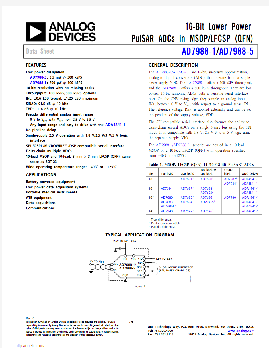
TYPICAL APPLICATION DIAGRAM
TO 5.5V
3- OR 4-WIRE INTERFACE
(SPI, DAISY CHAIN, CS)
1
2
3
1
-
1
Figure 1.
AD7988-1/AD7988-5
Data Sheet
Rev. C | Page 2 of 24
TABLE OF CONTENTS
Features .............................................................................................. 1 Applications ....................................................................................... 1 General Description ......................................................................... 1 Typical Application Diagram .......................................................... 1 Revision History ............................................................................... 2 Specifications ..................................................................................... 3 Timing Specifications .................................................................. 5 Absolute Maximum Ratings ............................................................ 7 ESD Caution .................................................................................. 7 Pin Configurations and Function Descriptions ........................... 8 Terminology ...................................................................................... 9 Typical Performance Characteristics ........................................... 10 Theory of Operation ...................................................................... 14 Circuit Information .................................................................... 14 Converter Operation .................................................................. 14 Typical Connection Diagram.................................................... 15 Analog Inputs.............................................................................. 16 Driver Amplifier Choice ........................................................... 16 Voltage Reference Input ............................................................ 17 Power Supply ............................................................................... 17 Digital Interface .......................................................................... 17 Mode, 3-Wire ........................................................................ 18 CS Mode 4-Wire ......................................................................... 19 Chain Mode ................................................................................ 20 Applications Information .............................................................. 21 Interfacing to Blackfin? DSP ..................................................... 21 Layout .......................................................................................... 21 Evaluating the Performance of the AD7988-x ........................ 21 Outline Dimensions ....................................................................... 22 Ordering Guide .. (23)
REVISION HISTORY
8/12—Rev. B to Rev. C
Changes to Ordering Guide (23)
5/12—Rev. A to Rev. B
Changes to Table 3 ............................................................................ 4 Updated Outline Dimensions . (22)
2/12—Rev. 0 to Rev. A
Added LFCSP Thermal Impedance Values ................................... 7 Updated Outline Dimensions ....................................................... 23 Changes to Ordering Guide . (23)
2/12—Revision 0: Initial Version
Data Sheet
AD7988-1/AD7988-5
Rev. C | Page 3 of 24
SPECIFICATIONS
VDD = 2.5 V , VIO = 2.3 V to 5.5 V , V REF = 5 V , T A = –40°C to +125°C, unless otherwise noted. Table 2.
Parameter Test Conditions/Comments Min Typ Max Unit RESOLUTION 16 Bits ANALOG INPUT
Voltage Range
IN+ ? IN? 0 V REF V Absolute Input Voltage IN+ ?0.1 V REF + 0.1 V
IN?
?0.1 +0.1 V Analog Input CMRR f IN = 1 kHz
60 dB Leakage Current at 25°C Acquisition phase 1
nA Input Impedance See the Analog Inputs section ACCURACY
No Missing Codes
16 Bits Differential Linearity Error V REF = 5 V ?0.9 ±0.4 +0.9 LSB 1
V REF = 2.5 V ±0.55 LSB 1 Integral Linearity Error V REF = 5 V ?1.25 ±0.6 +1.25 LSB 1
V REF = 2.5 V ±0.65 LSB 1 Transition Noise V REF = 5 V 0.6 LSB 1
V REF = 2.5 V 1.0 LSB 1 Gain Error, T MIN to T MAX 2
±2 LSB 1 Gain Error Temperature Drift ±0.35 ppm/°C Zero Error, T MIN to T MAX 2 ?0.5 ±0.08 +0.5 mV Zero Temperature Drift
0.54 ppm/°C Power Supply Sensitivity VDD = 2.5 V ± 5% ±0.1 LSB 1 THROUGHPUT AD7988-1
Conversion Rate VIO ≥ 2.3 V up to 85°C, VIO ≥ 3.3 V above 85°C up to 125°C
0 100 kSPS Transient Response Full-scale step 500 ns AD7988-5
Conversion Rate
VIO ≥ 2.3 V up to 85°C, VIO ≥ 3.3 V above 85°C up to 125°C
0 500 kSPS Transient Response Full-scale step 400 ns AC ACCURACY
Dynamic Range V REF = 5 V 92 dB 3
V REF = 2.5 V 87 dB 3 Oversampled Dynamic Range f O = 10 kSPS
111 dB 3 Signal-to-Noise Ratio, SNR f IN = 10 kHz, V REF = 5 V 90 91 dB 3
f IN = 10 kHz, V REF = 2.5 V 86.5 dB 3 Spurious-Free Dynamic Range, SFDR f IN = 10 kHz ?110 dB 3 Total Harmonic Distortion, THD f IN = 10 kHz
?114 dB 3 Signal-to-(Noise + Distortion), SINAD f IN = 10 kHz, V REF = 5 V 91.5 dB 3
f IN = 10 kHz, V REF = 2.5 V
87.0
dB 3
1 LSB means least significant bit. With the 5 V input range, 1 LSB is 76.3 μV.
2
See the Terminology section. These specifications include full temperature range variation, but not the error contribution from the external reference. 3
All specifications in dB are referred to a full-scale input FSR. Tested with an input signal at 0.5 dB below full scale, unless otherwise specified.
AD7988-1/AD7988-5
Data Sheet
Rev. C | Page 4 of 24
VDD = 2.5 V , VIO = 2.3 V to 5.5 V , V REF = 5 V , T A = –40°C to +125°C, unless otherwise noted. Table 3.
Parameter Test Conditions/Comments Min Typ Max Unit
REFERENCE
Voltage Range
2.4 5.1 V Load Current
V REF = 5 V 250 μA SAMPLING DYNAMICS ?3 dB Input Bandwidth
10 MHz Aperture Delay VDD = 2.5 V 2.0 ns DIGITAL INPUTS Logic Levels
V IL VIO > 3 V –0.3 0.3 × VIO V V IH VIO > 3 V 0.7 × VIO VIO + 0.3 V V IL VIO ≤ 3 V –0.3 0.1 × VIO V V IH VIO ≤ 3 V 0.9 × VIO VIO + 0.3 V I IL ?1 +1 μA I IH
?1 +1 μA DIGITAL OUTPUTS
Data Format Serial 16 bits straight binary
Pipeline Delay
Conversion results available immediately
after completed conversion
V OL I SINK = 500 μA 0.4 V V OH
I SOURCE = ?500 μA VIO ? 0.3 V POWER SUPPLIES VDD
2.375 2.5 2.625 V VIO
Specified performance 2.3 5.5 V VIO Range
1.8 5.5 V Standby Current 1, 2
VDD and VIO = 2.5 V, 25°C 0.35 nA AD7988-1 Power Dissipation 10 kSPS throughput 70 μW 100 kSPS throughput 700 μW
1 mW AD7988-5 Power Dissipation 500 kSPS throughput 3.5 5 mW
Energy per Conversion 7.0 nJ/sample TEMPERATURE RANGE
Specified Performance
T MIN to T MAX
?40 +125
°C
1 With all digital inputs forced to VIO or GND as required. 2
During the acquisition phase.
Data Sheet AD7988-1/AD7988-5
TIMING SPECIFICATIONS
VDD = 2.37 V to 2.63 V, VIO = 3.3 V to 5.5 V, ?40°C to +125°C unless otherwise stated. See Figure 2 and Figure 3 for load conditions.
Rev. C | Page 5 of 24
AD7988-1/AD7988-5
Data Sheet
Rev. C | Page 6 of 24
1.4V
TO SDO
1023
1-002
Figure 2. Load Circuit for Digital Interface Timing
1FOR VIO ≤ 3.0V, X = 90 AND Y = 10; FOR VIO > 3.0V X = 70, AND Y = 30.2MINIMUM V IH AND MAXIMUM V IL
USED. SEE DIGITAL INPUTS SPECIFICATIONS IN TABLE 3.
10231-003
Figure 3. Voltage Levels for Timing
Data Sheet
AD7988-1/AD7988-5
Rev. C | Page 7 of 24
ABSOLUTE MAXIMUM RATINGS
Table 5.
Parameter Rating Analog Inputs
IN+,1 IN?1 to GND ?0.3 V to V REF + 0.3 V or ±130 mA Supply Voltage
REF, VIO to GND ?0.3 V to +6 V VDD to GND ?0.3 V to +3 V VDD to VIO
+3 V to ?6 V
Digital Inputs to GND ?0.3 V to VIO + 0.3 V Digital Outputs to GND
?0.3 V to VIO + 0.3 V Storage Temperature Range ?65°C to +125°C Junction Temperature 150°C θJA Thermal Impedance
10-Lead MSOP 200°C/W 10-Lead LFCSP
80°C/W θJC Thermal Impedance
10-Lead MSOP 44°C/W 10-Lead LFCSP 15°C/W
Reflow Soldering
JEDEC Standard (J-STD-020)
1
See the Analog Inputs section.
Stresses above those listed under Absolute Maximum Ratings may cause permanent damage to the device. This is a stress rating only; functional operation of the device at these or any other conditions above those indicated in the operational
section of this specification is not implied. Exposure to absolute maximum rating conditions for extended periods may affect device reliability.
ESD CAUTION
AD7988-1/AD7988-5
Data Sheet
Rev. C | Page 8 of 24
PIN CONFIGURATIONS AND FUNCTION DESCRIPTIONS
REF
VDD IN+IN–GND 10231-004
Figure 4. 10-Lead MSOP Pin Configuration
NOTES
1. THE EXPOSED PAD CAN BE CONNECTED TO GND.
1REF 2
VDD 3IN+4IN–5
GND 10VIO
9SDI 8SCK 7SDO 6
CNV
10231-005
AD7988-1/AD7988-5
TOP VIEW (Not to Scale)
Figure 5. 10-Lead LFCSP (QFN) Pin Configuration
1
AI = analog input, DI = digital input, DO = digital output, and P = power.
Data Sheet
AD7988-1/AD7988-5
Rev. C | Page 9 of 24
TERMINOLOGY
Integral Nonlinearity Error (INL)
INL refers to the deviation of each individual code from a line drawn from negative full scale through positive full scale. The point used as negative full scale occurs ? LSB before the first code transition. Positive full scale is defined as a level 1? LSB beyond the last code transition. The deviation is measured from the middle of each code to the true straight line (see Figure 30). Differential Nonlinearity Error (DNL)
In an ideal ADC, code transitions are 1 LSB apart. DNL is the maximum deviation from this ideal value. It is often specified in terms of resolution for which no missing codes are guaranteed. Offset Error
The first transition should occur at a level ? LSB above analog ground (38.1 μV for the 0 V to 5 V range). The offset error is the deviation of the actual transition from that point. Gain Error
The last transition (from 111 … 10 to 111 … 11) should occur for an analog voltage 1? LSB below the nominal full scale (4.999886 V for the 0 V to 5 V range). The gain error is the deviation of the actual level of the last transition from the ideal level after the offset is adjusted out. Spurious-Free Dynamic Range (SFDR)
SFDR is the difference, in decibels (dB), between the rms amplitude of the input signal and the peak spurious signal. Effective Number of Bits (ENOB)
ENOB is a measurement of the resolution with a sine wave input. It is related to SINAD by the following formula:
ENOB = (SINAD dB ? 1.76)/6.02 and is expressed in bits.
Noise-Free Code Resolution
Noise-free code resolution is the number of bits beyond which it is impossible to distinctly resolve individual codes. It is calculated as
Noise-Free Code Resolution = log 2(2N /Peak-to-Peak Noise ) and is expressed in bits. Effective Resolution
Effective resolution is calculated as
Effective Resolution = log 2(2N /RMS Input Noise ) and is expressed in bits.
Total Harmonic Distortion (THD)
THD is the ratio of the rms sum of the first five harmonic components to the rms value of a full-scale input signal and is expressed in dB.
Dynamic Range
Dynamic range is the ratio of the rms value of the full scale to the total rms noise measured with the inputs shorted together. The value for dynamic range is expressed in dB. It is measured with a signal at ?60 dBFS to include all noise sources and DNL artifacts.
Signal-to-Noise Ratio (SNR)
SNR is the ratio of the rms value of the actual input signal to the rms sum of all other spectral components below the Nyquist frequency, excluding harmonics and dc. The value for SNR is expressed in dB.
Signal-to-(Noise + Distortion) Ratio (SINAD)
SINAD is the ratio of the rms value of the actual input signal to the rms sum of all other spectral components below the Nyquist frequency, including harmonics but excluding dc. The value for SINAD is expressed in dB.
Aperture Delay
Aperture delay is the measure of the acquisition performance. It is the time between the rising edge of the CNV input and when the input signal is held for a conversion.
Transient Response
Transient response is the time required for the ADC to accurately acquire its input after a full-scale step function is applied.
AD7988-1/AD7988-5
Data Sheet
Rev. C | Page 10 of 24
TYPICAL PERFORMANCE CHARACTERISTICS
VDD = 2.5 V , V REF = 5.0 V , VIO = 3.3 V , unless otherwise noted.
0–180FREQUENCY (kHz)
–20
–40–60–80–100–120–140
–160
A M P L I T U D E (d
B o f F U L L S
C A L E )
05010015020025010231-046
Figure 6. AD7988-5 FFT Plot, V REF = 5 V
0–180FREQUENCY (kHz)
–20
–40–60–80–100–120–140–160
A M P L I T U D E (d
B o f F U L L S
C A L E )
05010015020025010231-047
Figure 7. AD7988-5 FFT Plot, V REF = 2.5 V
0–180
FREQUENCY (kHz)
–20
–40–60–80–100–120–140–160
A M P L I T U D E (d
B o f F U L L S
C A L E )
0102030405010231-048
Figure 8. AD7988-1 FFT Plot, V REF = 5 V
0–180
FREQUENCY (kHz)
–20–40–60–80–100–120–140
–160
A M P L I T U D E (d
B o f F U L L S
C A L E )
010203040
50
10231-049
Figure 9. AD7988-1 FFT Plot, V REF = 2.5 V
1.25–1.25
CODE
I N L (L S B )
1.000.750.500.25–0.25–0.750–0.50–1.00
016384
327684915265536
10231-010
Figure 10. Integral Nonlinearity vs. Code, V REF = 5 V
1.25
1.00–1.25
–1.00
I N L (L S B )
0.750.500.25–0.25–0.750–0.50CODE
016384327684915265536
10231-011
Figure 11. Integral Nonlinearity vs. Code, V REF = 2.5 V
分销商库存信息:
ANALOG-DEVICES
AD7988-5BRMZ AD7988-1BCPZ-RL AD7988-1BCPZ-RL7 AD7988-5BCPZ-RL AD7988-5BCPZ-RL7AD7988-5BRMZ-RL7 AD7988-1BRMZ-RL7AD7988-1BRMZ EVAL-AD7988-5SDZ