
w
Digital Audio Hub CODEC
DESCRIPTION
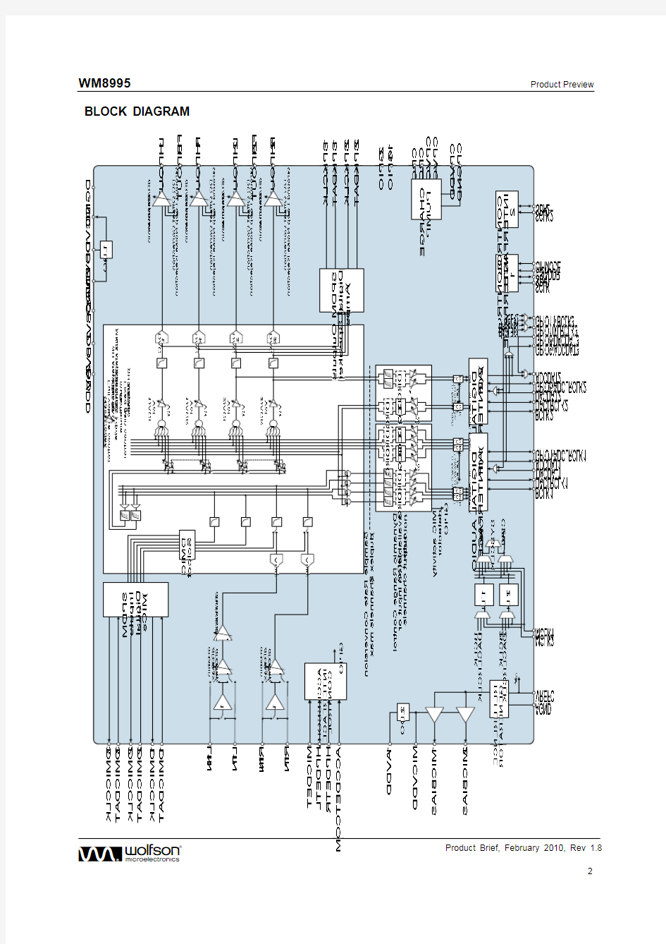
The WM8995 is a digital audio hub CODEC designed for smartphones. The device integrates two-wire SPDM interfaces for up to six digital microphones and four digital speaker amplifiers. All data, clocking and control of these remote transducers is managed using the SPDM interfaces. Four DAC channels and four ground-referenced class W output drivers provide interfaces to a headset connector, earpiece or line output. Ground loop feedback is employed to reduce common mode noise on these outputs. A low power accessory interface provides plug-in and removal detection and hookswitch button press detection in standby mode. Load impedance sensing circuits provide support for a wide range of 3.5mm accessory types. High PSRR, a fully differential internal architecture and on-chip RF noise filters ensure a very high degree of noise immunity. Stereo full duplex asynchronous sample rate converters are integrated to support digital mixing and loopback across asynchronous clock domains. The WM8995 is supplied in a very small and thin W-CSP package, ideal for portable systems.
AVDD1 AVDD2 LDO1ENA
WM8995
FEATURES
? ? ? ? ? 4-channel DAC with 100dB SNR (‘A’ weighted) 6-channel SPDM digital MIC interface 4-channel SPDM digital speaker interface Class W ground-referenced headphone/line outputs Headset connector interface Advanced accessory detect function Headphone common mode feedback Multi-channel digital audio interfaces - All standard data formats and 4-channel TDM supported - All standard sample rates from 8kHz to 96kHz - 192kHz ultrasonic MIC output mode - Sample rate conversion, digital mixing and loopback Low power dual FLL - Provides all necessary internal clocks - 32kHz to 27MHz input frequency with exact 8kHz support Dual control interface - Standard 2-wire control interface - Interrupts to DSP and application processor 69-ball W-CSP package (3.67 x 3.57 x 0.7mm, 0.4mm pitch)
?
? ? ?
APPLICATIONS
? Smartphones and music phones
DBVDD2 DBVDD3 DCVDD DGND DBVDD1
DMICCLK1 DMICDAT1 DMICCLK2 DMICDAT2 DMICCLK3 DMICDAT3
6-CHANNEL DIGITAL MIC INTERFACE
DAC L1
HPOUT1L HPOUT1FB
DAC R1
HPOUT1R
IN1LN IN1LP PGAs IN1RN IN1RP
ADC L DIGITAL MIXING CORE
DAC L2
HPOUT2L HPOUT2FB
ADC R
DAC R2
HPOUT2R
MICDET HPDETL HPDETR ACCDETCOM ACCESSORY INTERFACE MICVDD MICBIAS1 DIGITAL AUDIO ENHANCEMENTS 1 DIGITAL AUDIO ENHANCEMENTS 2 ASYNCHRONOUS SAMPLE RATE CONVERSION
4-CHANNEL DIGITAL SPEAKER AMPLIFIER INTERFACE
SPKCLK1 SPKDAT1 SPKCLK2 SPKDAT2 GPIO14 GPIO2
MICBIAS2
FLL2 MIXERS AND MULTIPLEXERS REFERENCE GENERATOR AUDIO INTERFACE 1 AUDIO INTERFACE 2 AUDIO INTERFACE 3 CONTROL INTERFACE1 CONTROL INTERFACE2 CHARGE PUMP CPCA CPCB CPVOUTP CPVOUTN
FLL1
WOLFSON MICROELECTRONICS plc
To receive regular email updates, sign up at https://www.doczj.com/doc/8513904084.html,/enews
AGND
VREFC
CPGND
CPVDD
MCLK2 MCLK1
ADCLRCLK1/GPIO1 ADCDAT1 DACDAT1 DACLRCLK1 BCLK1
ADCDAT2 GPIO6/ADCLRCLK2 DACDAT2 DACLRCLK2 BCLK2
GPIO11/BCLK3 GPIO10/LRCLK3 GPIO8/DACDAT3 GPIO9/ADCDAT3
CIFMODE CS/ADDR SDA1 SCLK1
Product Brief, February 2010, Rev 1.8
Copyright ?2010 Wolfson Microelectronics plc
SDA2 SCLK2
WM8995 BLOCK DIAGRAM
Product Preview
w
Product Brief, February 2010, Rev 1.8 2
Product Preview
WM8995
PIN CONFIGURATION
ORDERING INFORMATION
ORDER CODE WM8995ECSN/R Note: Reel quantity = 3500 TEMPERATURE RANGE -40°C to +85°C PACKAGE 69-ball W-CSP (Pb-free, Tape and reel) MOISTURE SENSITIVITY LEVEL MSL1 PEAK SOLDERING TEMPERATURE 260°C
w
Product Brief, February 2010, Rev 1.8 3
WM8995 PIN DESCRIPTION
PIN NO A1 A2 A3 A4 A5 A6 A7 A8 A9 B1 B2 B3 B4 B5 B6 B7 B8 B9 C1 C2 C3 C4 C5 C6 C7 C8 C9 D1 D2 D3 D7 D8 D9 E1 E2 E3 E7 E8 E9 F1 F2 F3 F8 F9 NAME GPIO9/ ADCDAT3 DBVDD3 DMICDAT2 DMICCLK3 DMICCLK1 DNC MICBIAS2 IN1LP IN1RP SPKCLK1 GPIO11/ BCLK3 DMICDAT3 DMICCLK2 MICBIAS1 DNC MICDET IN1LN AGND GPIO14 SPKDAT1 DMICDAT1 MICVDD VREFC AVDD1 IN1RN AVDD2 HPDETR SPKCLK2 SPKDAT2 GPIO10/ LRCLK3 ACCDETCOM HPDETL HPOUT1FB BCLK1 DACLRCLK1 GPIO8/ DACDAT3 HPOUT1R HPOUT1L HPOUT2R MCLK2 GPIO2 MCLK1 HPOUT2FB HPOUT2L Analogue Input Analogue Input Supply Digital Input / Output Digital Output Digital Input Supply / Analogue Output Analogue Output Supply Analogue Input Supply Analogue Input / Output Digital Output Digital Output Digital Input / Output Analogue Input / Output Analogue Input / Output Analogue Input Digital Input / Output Digital Input / Output Digital Input / Output Analogue Output Analogue Output Analogue Output Digital Input Digital Input / Output Digital Input Analogue Input Analogue Output Analogue Output Analogue Input Analogue Input Digital Output Digital Input / Output Digital Input Digital Output Analogue Output TYPE Digital Input / Output Supply Digital Input Digital Output Digital Output DESCRIPTION General Purpose pin GPIO 9 / Audio interface 3 ADC digital audio data Digital buffer (I/O) supply (for Audio Interface 3) Digital Microphone data input 2 Digital Microphone clock output 3 Digital Microphone clock output 3 Do not connect
Product Preview
Microphone bias 2 (for microphone / accessory detection circuit) Left channel non-inverting single-ended input / Left channel positive differential input Right channel non-inverting single-ended input / Right channel positive differential input Digital Speaker (PDM) clock output 1 General Purpose pin GPIO 11 / Audio interface 3 bit clock Digital Microphone data input 3 Digital Microphone clock output 2 Microphone bias 1 (digital microphone supply) Do not connect Microphone / accessory detect sense input Left channel inverting single-ended input / Left channel negative differential input Analogue ground (Return path for AVDD1, AVDD2, MICVDD) General Purpose pin GPIO 14 Digital Speaker (PDM) data output 1 Digital Microphone data input 2 Microphone supply / LDO2 output Bandgap reference decoupling capacitor LDO2 input Right channel inverting single-ended input / Right channel negative differential input Analogue core supply Headphone Right sense input Digital Speaker (PDM) clock output 2 Digital Speaker (PDM) data output 2 General Purpose pin GPIO 10 / Audio interface 3 left / right clock Headphone detect ground (Return path for HPDETL / HPDETR) Headphone Left sense input HPOUT1L and HPOUT1R ground loop noise rejection feedback Audio interface 1 bit clock Audio interface 1 DAC left / right clock (can also be used for ADC clock) General Purpose pin GPIO 8 / Audio interface 3 DAC digital audio data Right headphone 1 output Left headphone 1 output Right headphone 2 output Master clock 2 General Purpose pin GPIO 2 Master clock 1 HPOUT2L and HPOUT2R ground loop noise rejection feedback Left headphone 2 output Product Brief, February 2010, Rev 1.8 4
w
Product Preview PIN NO G1 G2 G3 G4 G5 G8 G9 H1 H2 H3 H4 H5 H6 H7 H8 H9 J1 J2 J3 J4 J5 J6 J7 J8 J9 NAME CIFMODE SCLK1 CS/ADDR ˉˉ SDA2 LDO1ENA CPVOUTP CPVOUTN SDA1 DCVDD DGND ADCDAT1 ADCDAT2 DACDAT2 BCLK2 CPCA CPCB SCLK2 DBVDD1 DACDAT1 ADCLRCLK1/ GPIO1 GPIO6/ ADCLRCLK2 DACLRCLK2 DBVDD2 CPVDD CPGND TYPE Digital Input Digital Input Digital Input Digital Input / Output Digital Input Analogue Output Analogue Output Digital Input / Output Supply / Analogue Output Supply Digital Output Digital Output Digital Input Digital Input / Output Analogue Output Analogue Output Digital Input Supply Digital Input Digital Input / Output Digital Input / Output Digital Input / Output Supply Supply Supply Control interface 1 clock input DESCRIPTION Control interface 1 mode select
WM8995
Control interface 1 3-/4-wire (SPI) chip select or 2-wire (I2C) address select Control interface 2 data input / acknowledge output Enable pin for LDO1 Charge pump positive supply decoupling pin (HPOUT1 / HPOUT2) Charge pump negative supply decoupling pin (HPOUT1 / HPOUT2) Control interface 1 data input / 2-wire acknowledge output Digital core supply / LDO1 output Digital ground (Return path for DCVDD, DBVDD1, DBVDD2, DBVDD3) Audio interface 1 ADC digital audio data Audio interface 2 ADC digital audio data Audio interface 2 DAC digital audio data Audio interface 2 bit clock Charge pump fly-back capacitor pin Charge pump fly-back capacitor pin Control interface 2 clock input Digital buffer (I/O) supply (core functions and Audio Interface 1) / LDO1 input Audio interface 1 DAC digital audio data Audio interface 1 ADC left / right clock / General Purpose pin GPIO 1 General Purpose pin GPIO 6 / Audio interface 2 ADC left / right clock Audio interface 2 DAC left / right clock (can also be used for ADC clock) Digital buffer (I/O) supply (for Audio Interface 2) Charge pump supply Charge pump ground (Return path for CPVDD)
w
Product Brief, February 2010, Rev 1.8 5
WM8995 ABSOLUTE MAXIMUM RATINGS
Product Preview
Absolute Maximum Ratings are stress ratings only. Permanent damage to the device may be caused by continuously operating at or beyond these limits. Device functional operating limits and guaranteed performance specifications are given under Electrical Characteristics at the test conditions specified. ESD Sensitive Device. This device is manufactured on a CMOS process. It is therefore generically susceptible to damage from excessive static voltages. Proper ESD precautions must be taken during handling and storage of this device. Wolfson tests its package types according to IPC/JEDEC J-STD-020B for Moisture Sensitivity to determine acceptable storage conditions prior to surface mount assembly. These levels are: MSL1 = unlimited floor life at <30°C / 85% Relative Humidity. Not normally stored in moisture barrier bag. MSL2 = out of bag storage for 1 year at <30°C / 60% Relative Humidity. Supplied in moisture barrier bag. MSL3 = out of bag storage for 168 hours at <30°C / 60% Relative Humidity. Supplied in moisture barrier bag. The Moisture Sensitivity Level for each package type is specified in Ordering Information. CONDITION Supply voltages (AVDD1, MICVDD, DBVDD2, DBVDD3) Supply voltages (AVDD2, DCVDD, DBVDD1) Supply voltages (CPVDD) Voltage range digital inputs (DBVDD1 domain) Voltage range digital inputs (DBVDD2 domain) Voltage range digital inputs (DBVDD3 domain) Voltage range analogue inputs Operating temperature range, TA Junction temperature, TJ Storage temperature after soldering MIN -0.3V -0.3V -0.3V DGND -0.3V DGND -0.3V DGND -0.3V AGND -0.3V -40oC -40oC -65oC MAX +4.5V +2.5V +2.2V DBVDD1 +0.3V DBVDD2 +0.3V DBVDD3 +0.3V AVDD2 +0.3V +85oC +150oC +150oC
RECOMMENDED OPERATING CONDITIONS
PARAMETER Digital supply range (Core) Digital supply range (I/O) Digital supply range (I/O) Analogue supply 1 range Analogue supply 2 range Charge Pump supply range Microphone Bias supply Ground Notes 1. All digital and analogue grounds must always be within 0.3V of each other. SYMBOL DCVDD DBVDD1 DBVDD2, DBVDD3 AVDD1 AVDD2 CPVDD MICVDD DGND, AGND, CPGND MIN 0.95 1.62 1.62 1.71 1.71 1.71 1.71 TYP 1.0 1.8 1.8 3.0 1.8 1.8 2.5 0 MAX 2.0 2.0 3.6 3.6 2.0 2.0 3.6 UNIT V V V V V V V V
w
Product Brief, February 2010, Rev 1.8 6
Product Preview
WM8995
PACKAGE DIMENSIONS
B: 69 BALL W-CSP PACKAGE 3.670 X 3.570 X 0.7mm BODY, 0.40 mm BALL PITCH DM076.A
6 2 A A2 A B C e D E F G H I 2X e 0.10 Z 0.10 Z f1 SOLDER BALL 5 E1 9 8 7 6 5 4 3 2 1 D
DETAIL 1
A1 CORNER 4
E
DETAIL 2
D1
2X
TOP VIEW
BOTTOM VIEW
f2
h 1 Z A1
DETAIL 2
Symbols A A1 A2 D D1 E E1 e f1 f2 h MIN 0.645 0.170 0.465 3.630 3.530
Dimensions (mm) NOM MAX 0.755 0.700 0.235 0.210 0.490 0.525 3.670 3.710 3.200 3.610 3.570 3.200 0.400
NOTE
5
0.215 0.165 0.221 0.258 0.295
NOTES: 1. PRIMARY DATUM -Z- AND SEATING PLANE ARE DEFINED BY THE SPHERICAL CROWNS OF THE SOLDER BALLS. 2. THIS DIMENSION INCLUDES STAND-OFF HEIGHT ‘A1’ AND BACKSIDE COATING. 3. A1 CORNER IS IDENTIFIED BY INK/LASER MARK ON TOP PACKAGE. 4. BILATERAL TOLERANCE ZONE IS APPLIED TO EACH SIDE OF THE PACKAGE BODY. 5. ‘e’ REPRESENTS THE BASIC SOLDER BALL GRID PITCH. 6. THIS DRAWING IS SUBJECT TO CHANGE WITHOUT NOTICE. 7. FOLLOWS JEDEC DESIGN GUIDE MO-211-C.
w
Product Brief, February 2010, Rev 1.8 7
WM8995 IMPORTANT NOTICE
Product Preview
Wolfson Microelectronics plc (“Wolfson”) products and services are sold subject to Wolfson’s terms and conditions of sale, delivery and payment supplied at the time of order acknowledgement.
Wolfson warrants performance of its products to the specifications in effect at the date of shipment. Wolfson reserves the right to make changes to its products and specifications or to discontinue any product or service without notice. Customers should therefore obtain the latest version of relevant information from Wolfson to verify that the information is current.
Testing and other quality control techniques are utilised to the extent Wolfson deems necessary to support its warranty. Specific testing of all parameters of each device is not necessarily performed unless required by law or regulation.
In order to minimise risks associated with customer applications, the customer must use adequate design and operating safeguards to minimise inherent or procedural hazards. Wolfson is not liable for applications assistance or customer product design. The customer is solely responsible for its selection and use of Wolfson products. Wolfson is not liable for such selection or use nor for use of any circuitry other than circuitry entirely embodied in a Wolfson product.
Wolfson’s products are not intended for use in life support systems, appliances, nuclear systems or systems where malfunction can reasonably be expected to result in personal injury, death or severe property or environmental damage. Any use of products by the customer for such purposes is at the customer’s own risk.
Wolfson does not grant any licence (express or implied) under any patent right, copyright, mask work right or other intellectual property right of Wolfson covering or relating to any combination, machine, or process in which its products or services might be or are used. Any provision or publication of any third party’s products or services does not constitute Wolfson’s approval, licence, warranty or endorsement thereof. Any third party trade marks contained in this document belong to the respective third party owner.
Reproduction of information from Wolfson datasheets is permissible only if reproduction is without alteration and is accompanied by all associated copyright, proprietary and other notices (including this notice) and conditions. Wolfson is not liable for any unauthorised alteration of such information or for any reliance placed thereon.
Any representations made, warranties given, and/or liabilities accepted by any person which differ from those contained in this datasheet or in Wolfson’s standard terms and conditions of sale, delivery and payment are made, given and/or accepted at that person’s own risk. Wolfson is not liable for any such representations, warranties or liabilities or for any reliance placed thereon by any person.
ADDRESS:
Wolfson Microelectronics plc 26 Westfield Road Edinburgh EH11 2QB United Kingdom
Tel :: +44 (0)131 272 7000 Fax :: +44 (0)131 272 7001 Email :: sales@https://www.doczj.com/doc/8513904084.html,
w
Product Brief, February 2010, Rev 1.8 8