
TRF3750
SLWS146B ? MARCH 2004 ? REVISED AUGUST 2007
HIGH-PERFORMANCE INTEGER-N PLL FREQUENCY SYNTHESIZER
FEATURES
D Single Device Covers Frequencies Up to
2.4GHz
D Dual Supply Range: 3 V ? 3.6 V and
4.5 V ?
5.5V
D Separate Charge Pump Supply (V CP) Up
to 8V
D Simple 3-Wire Serial Interface Allows for Fully
Programmable:
? A, B, and R Counters
? Dual Modulus Prescaler [8/9, 16/17, 32/33,
and 64/65]
? Charge Pump Current
D Lock Detect Output (Digital and Analog)
D Versatile Hardware and Software Power Down D Packaged in a 16-Pin TSSOP Thin Quad
FlatPack and a 20-Pin 4 x 4 mm QFN Package APPLICATIONS
D Wireless Infrastructure
? GSM, IS136, EDGE/UWC?136
? IS95, UMTS, CDMA2000
D Portable Wireless Communications
D Wireless LAN
D Wireless Transceivers
D Communication Test Equipment DESCRIPTION
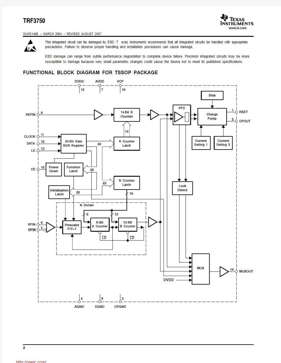
The TRF3750 frequency synthesizer is ideal for designing the local os cillator portion of wireless transceivers by providing complete programmability and ultra-low phase noise. The device features a user-selectable dual-modulus prescaler, a 14-bit reference (R) divider, a 6-bit A,and a 13-bit B counter. The R divider allows the user to select the frequency of choice for the phase-frequency detector (PFD) circuit, and with the use of the counters implement an N divider of value N = A + P x B. With an extended charge-pump supply (V CP) of up to 8 V, a wide variety of external VCOs can be used to complete the phase-locked loop. Ultra-low phase noise and reference spur performance make the TRF3750 ideal for generating the local oscillator in the most demanding wireless applications.
RSET
CPOUT
CPGND
AGND
RFIN
RFIN
AVDD
REFIN
VCP
DVDD
MUXOUT
LE
DATA
CLOCK
CE
DGND
PW PACKAGE
(TOP VIEW)
MUXOUT
RGP PACKAGE
(TOP VIEW)
CPGND
C
P
O
U
T
R
S
E
T
V
C
P
D
V
D
D
D
V
D
D
R
E
F
I
N
D
G
N
D
A
V
D
D
1
2
3
4
5
15
14
13
12
11
678910
2019181716
A
V
D
D
D
G
N
D
LE
DATA
CLOCK
CE
RFIN
RFIN
AGND
AGND
PRODUCTION DATA information is curre nt as of publication date. Products
conform to specifications per the terms of Texas Instruments standard warranty.
Production processing does not necessarily include testing of all parameters.
Please be aware that an important notice concerning availability, standard warranty, and use in critical applications of T exas Instruments semiconductor products and disclaimers thereto appears at the end of this data sheet.
https://www.doczj.com/doc/8412727823.html,
Copyright ? 2007, Texas Instruments Incorporated
TRF3750
SLWS146B ? MARCH 2004 ? REVISED AUGUST 2007
https://www.doczj.com/doc/8412727823.html,
2
This integrated circuit can be damaged by ESD. T exas Instruments recommends that all integrated circuits be handled with appropriate precautions. Failure to observe proper handling and installation procedures can cause damage.
ESD damage can range from subtle performance degradation to complete device failure. Precision integrated circuits may be more susceptible to damage because very small parametric changes could cause the device not to meet its published specifications.
FUNCTIONAL BLOCK DIAGRAM FOR TSSOP PACKAGE
MUXOUT
RSET CPOUT
AGND
DGND
CPGND
TRF3750
SLWS146B ? MARCH 2004 ? REVISED AUGUST 2007
https://www.doczj.com/doc/8412727823.html,
3
ORDERING INFORMATION
PRODUCT PACKAGE /LEADS PACKAGE DESIGNATOR
SPECIFIED TEMPERATURE
RANGE PACKAGE MARKING ORDERING NUMBER TRANSPORT MEDIA
QUANTITY
TRF3750IPW TSSOP-16PW –40°C to 85°C TRF3750TRF3750IPW Tube 90TRF3750IPWR TSSOP-16PW –40°C to 85°C TRF3750TRF3750IPWR Reel 2000TRF3750IRGP QFN-20RGP –40°C to 85°C TRF3750TRF3750IRGP Tube 91TRF3750IRGPR
QFN-20
RGP
–40°C to 85°C
TRF3750
TRF3750IRGPR
Reel
1000
PIN ASSIGNMENTS
(1)
The thermal pad on the bottom of the QFN package may be tied to ground, but is not required to meet specified performance.
TRF3750
SLWS146B ? MARCH 2004 ? REVISED AUGUST 2007
https://www.doczj.com/doc/8412727823.html,
4
ABSOLUTE MAXIMUM RATINGS
over operating free-air temperature range unless otherwise noted (1)
UNIT
AVDD
?0.3 V to 6.5 V Supply voltage range (2)
AVDD to DVDD ?0.3 V to 0.3 V VCP to AGND
?0.3 V to 9 V Digital I/O voltage to DGND (DGND = 0 V)?0.3 V to 6.5 V Reference signal input REFIN to DGND ?0.3 V to DVDD + 0.3 V
RF prescaler input RFIN, RFIN to AGND
?0.3 V to 6.5 V
Continuous power dissipation
See Dissipation Rating T able
Storage temperature, T Stg
?65°C to 150°C
Lead temperature 1,6 mm (1/16 inch) from case for 10 seconds
260°C
(1)
Stresses beyond those listed under “absolute maximum ratings” may cause permanent damage to the device. These are stress ratings only, and functional operation of the device at these or any other conditions beyond those indicated under “recommended operating conditions” is not implied. Exposure to absolute-maximum-rated conditions for extended periods may affect device reliability.(2)All voltage values are with respect to network ground terminal.
DISSIPATION RATING TABLE
PACKAGE T A ≤ 25°C DERATING FACTOR (1)ABOVE T A = 25°C
T A = 85°C POWER RATING
16-pin TSSOP 2780 mW 22.2 mW/_C 1440 mW 20-pin QFN
2780 mW
29 mW/_C
1440 mW
(1)
This is the inverse of the junction-to-ambient thermal resistance when board mounted and with no airflow.
RECOMMENDED OPERATING CONDITIONS
MIN
NOM MAX UNIT AVDD = DVDD, 3.3 V range
3 3.3 3.6V AVDD = DVDD, 5 V range 4.5
5
5.5V Supply voltage
VCP
(AVDD, DVDD) + 1
8
V High ?level input voltage, V IH LE DATA CLK CE 0.8 x DVDD
V Low ?level input voltage, V IL LE, DATA, CLK, CE 0.2 x DVDD
V High ?level output voltage, V OH DVDD ? 0.4
V Low ?level output voltage, V OL MUXOUT
0.4
V Operating free-air temperature, T A
?40
85
°C
TRF3750
SLWS146B ? MARCH 2004 ? REVISED AUGUST 2007
https://www.doczj.com/doc/8412727823.html,
5
ELECTRICAL CHARACTERISTICS
Conditions: (AVDD = DVDD = 3.3 V or 5 V, AVDD + 1≤ VCP ≤ 8 V, R SET = 4.7 k ?, T A = ?40°C to 85°C, REFIN = 10MHz at +5 dBm) (unless otherwise stated)
PARAMETER
TEST CONDITIONS
MIN TYP MAX UNIT AVDD = 3.3 V 10I AVDD Supply current AVDD = 5 V 13mA DVDD = 3.3 V 3I DVDD Supply current DVDD = 5 V 3.5mA I VCP
Supply current
VCP = 7 V
7.5
mA
RFIN input frequency (RF input)2400
MHz RFIN input power level
?15+5dBm RF prescaler output frequency (1)
200MHz REFIN input frequency (reference input) (1)4
200
MHz REFIN input power level sensitivity ?10dBm REFIN input capacitance 5
pF PFD maximum frequency (1)
60
MHz I CPOUT max Charge pump max source current 5mA I CPOUT min Charge pump max sink current ?5
mA VTUNE
Output tuning voltage (2)
Measured at the output of the external loop filter, in locked condition
1
VCP ?1.1
V
(1)Assured by design.
(2)
VTUNE range shown is for optimal spurious performance; the device can function beyond these limits.
TRF3750
SLWS146B ? MARCH 2004 ? REVISED AUGUST 2007
https://www.doczj.com/doc/8412727823.html,
6
ELECTRICAL CHARACTERISTICS
Conditions (unless otherwise stated): AVDD = DVDD = 3.3 V or 5 V, VCP = 7 V; R SET = 4.7 k ?, T A = 27°C, REFIN = 10 MHz at 6.5 dBm Referenced to 50 ?, I CPOUT max = 5 mA, Power Down: Normal Operation; Timer Counter Control: Not used; MUXOUT Control: 3-state; Fast Lock Mode: Disabled, PFD Polarity: Positive, Anti-backlash Pulse width: 1.5 ns, Resync/Delay: Normal (Delay=0, Resync=0), Counter Operation: Normal, Charge Pump Output: Normal, Lock Detect Precision: 5 cycles
PARAMETER
TEST CONDITIONS
MIN
TYP MAX
UNIT Phase noise 110 MHz)PFD = 200 kHz, Loop Loop BW = 20 kHz, N 550 Phase noise measured at 1kHz offset ?106dBc/Hz Reference spurs 110 MHz N =550, Phase noise measured at 1-kHz offset spurs measured at ±PFD, ±2 x PFD ?110dBc Phase noise 300 MHz PFD = 200 kHz, Loop Loop BW = 20 kHz, N 1500 Phase noise measured at 1kHz ?99dBc/Hz Reference spurs 300 MHz N =1500, Phase noise measured at 1-kHz offset spurs measured at ±PFD, ±2 x PFD ?110dBc Phase noise 540 MHz PFD = 200 kHz, Loop Loop BW = 20 kHz, N 2700 Phase noise measured at 1kHz ?94dBc/Hz Reference spurs 540 MHz N = 2700, Phase noise measured at 1-kHz offset spurs measured at ±PFD, ±2 x PFD ?90dBc Phase noise 836 MHz PFD = 200 kHz, Loop Loop BW = 20 kHz, N 4180 Phase noise measured at 1kHz ?91dBc/Hz Reference spurs 836 MHz N = 4180, Phase noise measured at 1-kHz offset spurs measured at ±PFD, ±2 x PFD ?100dBc Phase noise 900 MHz
PFD = 200 kHz, Loop Loop BW = 20 kHz, N 4500 Phase noise measured at 1?91Phase noise 900 MHz, over temperature and supply N = 4500, Phase noise measured at 1?kHz offset spurs measured at ±PFD, ±2 x PFD ?90dBc/Hz Reference spurs 900 MHz
PFD = 200 kHz, Loop Loop BW = 20 kHz, N 4500 Phase noise measured at 1kHz ?100dBc Reference spurs 900 MHz, over temperature and supply N = 4500, Phase noise measured at 1-kHz offset spurs measured at ±PFD, ±2 x PFD ?100dBc Phase noise 1750 MHz PFD = 200 kHz, Loop Loop BW = 20 kHz, ?84dBc/Hz Reference spurs 1750 MHz N = 8750
Phase noise measured at 1-kHz offset spurs measured at ±PFD, ±2 x PFD
?96dBc Phase noise 1960 MHz
PFD = 200 kHz, Loop Loop BW = 20 kHz, N 9800 Phase noise measured at 1kHz ?84Phase noise 1960 MHz, over temperature and supply N = 9800, Phase noise measured at 1-kHz offset spurs measured at ±PFD, ±2 x PFD ?82dBc/Hz Reference spurs 1960 MHz
PFD = 200 kHz, Loop Loop BW = 20 kHz, N 9800 Phase noise measured at 1kHz ?90dBc Reference spurs 1960 MHz, over temperature and supply N = 9800, Phase noise measured at 1-kHz offset spurs measured at ±PFD, ±2 x PFD ?90dBc Phase noise 2200 MHz PFD = 200 kHz, Loop Loop BW = 20 kHz, N 11000 Phase noise measured at 1kHz ?83dBc/Hz Reference spurs 2200 MHz
N = 11000, Phase noise measured at 1-kHz offset spurs measured at ±PFD, ±2 x PFD
?90
dBc
TRF3750
SLWS146B ? MARCH 2004 ? REVISED AUGUST 2007
https://www.doczj.com/doc/8412727823.html,
7
PRODUCT TIMING CHARACTERISTICS
AVDD =DVDD =3.3V ±10% or 5V ±10%, T A = ?40°C to 85°C (unless otherwise stated)
PARAMETER
TEST CONDITIONS
MIN TYP
MAX
UNIT t (CLK)Clock period (1)50ns t su1Data setup time (2)10
ns t h Data hold time (2)10ns t w LE pulse width (2)20ns t su2
LE setup time (2)
10
ns
Production tested.(2)
Assured by design.
DATA
CLOCK
LE
Figure 1. Serial Programming Timing Diagram
TRF3750
SLWS146B ? MARCH 2004 ? REVISED AUGUST 2007
https://www.doczj.com/doc/8412727823.html,
8
TYPICAL CHARACTERISTICS
(Conditions are based on Electrical Characteristics table on page 6, unless otherwise noted)
f ? Frequency Offset from 110 MHz Carrier ? kHz ?120
?110
?100?90?80?70?60?50?40?30?20?100?500?400?300?200?1000
100200300400500
P O ? O u t p u t P o w e r ? d B c
OUTPUT POWER
vs
FREQUENCY
Figure 2. Reference Spurs
(RFOUT = 110 MHz)
Figure 3. Integrated Phase Noise
(RFOUT = 110 MHz)
?140
?130?120?110?100
?90?80?70?60?50?40P h a s e N o i s e ? d B c /H z
PHASE NOISE
vs
FREQUENCY
f ? Frequency Offset from 300 MHz Carrier ? kHz ?120
?110
?100?90?80?70?60?50?40?30?20?100?
P O ? O u t p u t P o w e r ? d B c
OUTPUT POWER
vs
FREQUENCY
Figure 4. Reference Spurs
(RFOUT = 300 MHz)?140
?130?120?110?100?90?80?70?60?50?40P h a s e N o i s e ? d B c /H z
PHASE NOISE
vs
FREQUENCY
Figure 5. Integrated Phase Noise
(RFOUT = 300 MHz)
TRF3750
SLWS146B ? MARCH 2004 ? REVISED AUGUST 2007
https://www.doczj.com/doc/8412727823.html,
9
TYPICAL CHARACTERISTICS
f ? Frequency Offset from 540 MHz Carrier ? kHz ?120
?110
?100?90?80?70?60?50?40?30?20?100?500?400?300?200?1000
100200300400500
P O ? O u t p u t P o w e r ? d B c
OUTPUT POWER
vs
FREQUENCY
Figure 6. Reference Spurs
(RFOUT = 540 MHz)
?140
?130?120?110?100?90
?80?70?60?50?40P h a s e N o i s e ? d B c /H z
PHASE NOISE
vs
FREQUENCY
Figure 7. Integrated Phase Noise
(RFOUT = 540 MHz)
f ? Frequency Offset from 836 MHz Carrier ? kHz ?120
?110
?100?90?80?70?60?50?40?30?20?100?500?400?300?200?1000
100200300400
500
P O ? O u t p u t P o w e r ? d B c
OUTPUT POWER
vs
FREQUENCY
Figure 8. Reference Spurs
(RFOUT = 836 MHz)?140
?130?120?110?100?90?
80?70?60?50?40P h a s e N o i s e ? d B c /H z
PHASE NOISE
vs
FREQUENCY
Figure 9. Integrated Phase Noise
(RFOUT = 836 MHz)
TRF3750
SLWS146B ? MARCH 2004 ? REVISED AUGUST 2007
https://www.doczj.com/doc/8412727823.html,
10
TYPICAL CHARACTERISTICS
f ? Frequency Offset from 900 MHz Carrier ? kHz
?120
?110
?100?90?80?70?60?50?40?30?20?100?500?400?300?200?1000
100200300400500
P O ? O u t p u t P o w e r ? d B c
OUTPUT POWER
vs
FREQUENCY
Figure 10. Reference Spurs
(RFOUT = 900 MHz)
f ? Frequency Offset from 900 MHz Carrier ? kHz
?100
?90
?80?70?60?50?40?30?20?100
?2.5?2.0?1.5?1.0?0.50.00.5 1.0 1.5 2.0
2.5
P O ? O u t p u t P o w e r ? d B c
OUTPUT POWER
vs
FREQUENCY
Figure 11. Phase Noise (RFOUT = 900 MHz)
?140
?130?120?110?100?90?
80?70?60?50?40P h a s e N o i s e ? d B c /H z
PHASE NOISE
vs
FREQUENCY
Figure 12. Integrated Phase Noise
(RFOUT = 900 MHz) f ? Frequency Offset from 1750 MHz Carrier ? kHz
?120
?110
?100?90?80?70?60?50?40?30?20?100?500?400?300?200?1000
100200300400500
P O ? O u t p u t P o w e r ? d B c
OUTPUT POWER
vs
FREQUENCY
Figure 13. Reference Spurs
(RFOUT = 1750 MHz)
分销商库存信息:
TI
TRF3750Q1900EVM TRF3750T-1900EVM