BulletProof A defect-tolerant cmp switch architecture
- 格式:pdf
- 大小:460.61 KB
- 文档页数:12
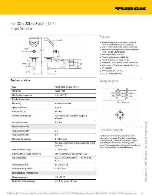
00-300L -30-2L I -H 1141 | 02/03/2020 14-08 | t e c h n i c a l c h a n g e s r e s e r v e d FS100-300L-30-2LI-H1141Flow SensorTechnical dataFS100-300L-30-2LI-H1141100001034Medium temperature-25…+85 °C Application areaImmersion sensorApplication area liquids Bar length (L1)45 mmImmersion depth (L)16.9 mm(when using the supplied adapter) Process Pressure300 barFlow MonitoringResponse time T096 s Response time T053 sStandard flow range3…300 cm/sAny axial alignment of the sensor rod in the mediumExtended flow range1…300 cm/sExtended flow range comment Directed inflow to punch mark ±20 °Reproducibility 0.2…5 cm/s; for water 3…100 cm/s; 10…80 °C Temperature drift 0.5 cm/s × 1/K Temperature gradient≤ 300 K/min Temperature monitoringMeasuring range -25…85 °CFeatures■Screw-in adapter with process connection G1/2’’ male thread included in delivery ■M18 × 1.5 female to G1/2 inch male thread ■Electronics housing material/medium contact 1.4404 (316L)/1.4571 (316Ti)■Immersion depth 16.9 mm■Process value display via LED bar ■Flow monitoring for liquid media■Protection classes IP6K6K, IP6K7 and IP6K9K ■Adjustment of flow speed via teach function ■17…33 VDC■Analog output 4…20 mA ■M12 × 1 male connectorWiring diagramFunctional principleThe flow sensor functions according to thecalorimetric principle. The distinctive feature of this principle is that the flow rate correlates directly to the thermal loss of energy in theprobe. The increased loss of energy is therefore a direct measure of an increased flow rate.00-300L -30-2L I -H 1141 | 02/03/2020 14-08 | t e c h n i c a l c h a n g e s r e s e r v e d Technical data00-300L -30-2L I -H 1141 | 02/03/2020 14-08 | t e c h n i c a l c h a n g e s r e s e r v e dTechnical dataMounting instructions00-300L -30-2L I -H 1141 | 02/03/2020 14-08 | t e c h n i c a l c h a n g e s r e s e r v e dsensors without a switching output only have MAX/MIN Teach.00-300L -30-2L I -H 1141 | 02/03/2020 14-08 | t e c h n i c a l c h a n g e s r e s e r v e d LED displayLED ColorStatusDescriptionPWR GreenOnOperating voltage applied Device is operational FLT Red On Error displayed(for error pattern in combination with LEDs see manual)Off No errors displayed LOC Yellow On Device locked OffDevice unlockedFlashing Locking/unlocking process activeFLOW Yellow Flashing Teach mode/display of diagnostic data (see manual for specification)TEMPYellowFlashingTeach mode/display of diagnostic data (see manual for specification)For a detailed description of the display patterns and flashing codes see manual/operating instructions FS100 — compact flow sensors (D100002658)Accessories Wiring accessoriesDimension drawingTypeIdent. no.RKC4.4T-2/TEL6625013Connection cable, female M12, straight,4-pin, cable length: 2 m, sheath material:PVC, black; cULus approval; other cable lengths and qualities available, see WKC4.4T-2/TEL 6625025Connection cable, female M12, angled,4-pin, cable length: 2 m, sheath material:PVC, black; cULus approval; other cable lengths and qualities available, see Accessories。


As a programmer,writing an English report can be a critical task,especially when it comes to communicating technical details,project progress,or issues to stakeholders who may not be as familiar with the intricacies of coding.Heres a detailed guide on how to write an effective English report for programmers:1.Title:Start with a clear and concise title that summarizes the content of the report.For example,Project X Development Progress Report.2.Introduction:Briefly introduce the purpose of the report.Mention the projects name and its objectives.State the reports scope and the period it covers.3.Project Overview:Provide a brief description of the project.Outline the main goals and deliverables.Mention the team members and their roles.4.Development Progress:Detail the progress made since the last report or since the projects inception.Use bullet points or numbered lists to organize the information.Include specific features or functionalities that have been implemented.5.Technical Details:Describe any technical challenges faced and how they were overcome.Explain the technologies used,including programming languages,frameworks,and tools.Provide code snippets or diagrams if necessary to illustrate complex concepts.6.Testing and Quality Assurance:Discuss the testing strategies employed,including unit tests,integration tests,and user acceptance testing.Mention the results of the tests and any issues that were identified.7.Project Milestones:List the major milestones achieved,including deadlines met and deliverables completed.Highlight any upcoming milestones or deadlines.8.Issues and Risks:Identify any current issues or risks that may impact the projects timeline or quality. Discuss the steps being taken to mitigate these risks.9.Team Performance:Evaluate the performance of the development team.Mention any challenges in team dynamics and how they are being addressed.10.Future Plans:Outline the next steps or phases of the project.Provide a tentative schedule for upcoming tasks and milestones.11.Conclusion:Summarize the key points of the report.Reiterate the projects current status and future outlook.12.Appendices:Include any additional documentation,such as detailed technical specifications,user manuals,or supplementary data.13.References:List any external sources or references used in the report.14.Formatting and Language:Use clear and professional language.Ensure consistency in formatting,such as font size,headings,and bullet points. Proofread the report for grammar and spelling errors.15.Distribution:Specify who the report is intended for,such as project managers,team members,or clients.Include a distribution list if necessary.Remember,the goal of a programmers report is to communicate complex information in a clear,concise,and accessible manner.Tailor the level of technical detail to your audiences understanding and ensure that the report is easy to navigate with a logical flow of information.。

美丽心灵英文剧本台词.txt人生重要的不是所站的位置,而是所朝的方向。
不要用自己的需求去衡量别人的给予,否则永远是抱怨。
看电影学英语 A Beautiful Mind 《美丽心灵》-Professor: Mathematicians won the war. Mathematicians broke the Japanese codes, and built the A-bomb.mathematician: 数学家 break: 破译(密码) code: 密码 a-bomb: 原子弹是数学家赢得了二次大战。
是数学家破解了日本的密码,建造了原子炸弹。
Mathematicians... like you. The stated goal of the Soviets is global Communism stated: 陈述的,说明的,决定了的 goal: 目标 Soviet: 苏联 global: 全球的,全世界的communism: 共产主义就是……像你们这样的数学家。
苏联所定的目标是让共产党布遍全球。
In medicine or economics, in technology or space, battle lines are being drawn. medicine: 医学,医药 economics: 经济学 technology: 科技 space: 宇宙,太空 battle: 战争 line: 线 drawn: draw的过去分词,描写,刻画无论在医药还是经济上,在科技或太空技术上,战线已经分明了。
To triumph, we need results- publishable, applicable results.triumph: 得胜,成功 result: 结果,成绩 publishable: 可发表的,可出版的 applicable: 可应用的,实用的想要胜利,我们就需要有成果—可以发表,实用的成果。
+plus加号;正号-minus减号;负号±plus or minus正负号×is multiplied by乘号÷is divided by除号=is equal to等于号≠is not equal to不等于号≡is equivalent to全等于号≌is equal to or approximately equal to等于或约等于号≈is approximately equal to约等于号<is less than小于号>is more than大于号≮is not less than不小于号≯is not more than不大于号≤is less than or equal to小于或等于号≥is more than or equal to大于或等于号%per cent百分之…‰per mill千分之…∞infinity无限大号∝varies as与…成比例√(square) root平方根∵since; because因为∴hence所以∷equals, as (proportion)等于,成比例∠angle角⌒semicircle半圆⊙circle圆○circumference圆周πpi 圆周率△triangle三角形⊥perpendicular to垂直于∪union of并,合集∩intersection of 交,通集∫the integral of …的积分∑(sigma) summation of总和°degree度′minute分″second秒℃Celsius system摄氏度{open brace, open curly左花括号}close brace, close curly右花括号(open parenthesis, open paren左圆括号)close parenthesis, close paren右圆括号() brakets/ parentheses括号[open bracket 左方括号]close bracket 右方括号[] square brackets方括号.period, dot句号,点|vertical bar, vertical virgule竖线& amp;ampersand, and, reference, ref和,引用*asterisk, multiply, star, pointer星号,乘号,星,指针/slash, divide, oblique 斜线,斜杠,除号//slash-slash, comment 双斜线,注释符#pound井号\backslash, sometimes escape反斜线转义符,有时表示转义符或续行符~tilde波浪符.full stop句号,comma逗号:colon冒号;semicolon分号?question mark问号!exclamation mark (英式英语) exclamation point (美式英语)'apostrophe撇号-hyphen连字号-- dash 破折号...dots/ ellipsis省略号"single quotation marks 单引号""double quotation marks 双引号‖parallel 双线号~swung dash 代字号§section; division 分节号→arrow 箭号;参见号break 跳出当前循环case 开关语句分支char 声明字符型变量或函数const 声明只读变量continue 结束当前循环,开始下一轮循环default 开关语句中的“其他”分支do 循环语句的循环体double 声明双精度变量或函数else 条件语句否定分支(与 if 连用)enum 声明枚举类型extern 声明变量是在其他文件正声明(也可以看做是引用变量)float 声明浮点型变量或函数for 一种循环语句(可意会不可言传)goto 无条件跳转语句if 条件语句inlineint 声明整型变量或函数long 声明长整型变量或函数register 声明积存器变量restrictreturn 子程序返回语句(可以带参数,也看不带参数)short 声明短整型变量或函数signed 生命有符号类型变量或函数sizeof 计算数据类型长度static 声明静态变量struct 声明结构体变量或函数switch 用于开关语句typedef 用以给数据类型取别名(当然还有其他作用)union 声明联合数据类型unsigned 声明无符号类型变量或函数void 声明函数无返回值或无参数,声明无类型指针(基本上就这三个作用)volatile 说明变量在程序执行中可被隐含地改变while 循环语句的循环条件C++语言中常用的关键字、类名、函数及其他常用单词main主要的,主函数bool定义布尔型变量break跳出循环或switch语句case switch语句中使用char 定义字符型变量class 定义类const 定义常量continue 继续,结束本次循环default 缺省的,用于switch语句delete 释放由new分配的内存do 执行,do while循环double 定义双精度实型变量if else 如果。

31. There are problems associated with providing a bad experience to a customer. The customercan turn on you. A term associated with this is:A) Defector B) T erroristC) Marginal D) Piranha39. If the project internal rate of return is estimated to be 11% andI) The company cost of capital is 10%II) The company cost of capital is 12%III) Funds are limited and another project will yield 14%IV) Funds are unlimited and another project will yield 14%A) I and III are true B) I and IV are trueC) II and III are true D) II and IV are true48. Advantages of computer software driven project management methods include:I) Ability to analyze "What-if" optionsII) Automatic calculation of the critical pathIII) The effects of actual results on the project are knownIV) Training requirements are minimalA) I, II and III only B) II, III and IV onlyC) II and III only D) I, II, III and IV75. In the six sigma define step, the critical to quality tree is used by the project team. the variouslevels of the tree are determined EXCEPT for:A) The exact metrics for the customerB) The needs of the customerC) The basic drivers for the customerD) The potential third level CTQ metrics79. If you are reading this question you are a customer of QCI, Identify QCI process outputelements from the list below:I) Binder suppliersII) Solution textsIII) AuthorsIV) Paper suppliersV) LibrariesVI) Question CDsVII) Study PrimersA) II, VI and VII only B) I and IV onlyC) III and V only D) II, III and VII only84. The probability of Steven passing his math course is 0.7, the probability of Steve passing hishistory class is 0.8. if the probability of Steve passing both course is 0.56, what is theprobability Steve will pass either math or history?A) 0 B) 1C) 0.99 D) 0.8485. The hypergeometric distribution should be used instead of the binomial distribution when:A) There are more than 2 outcomes on a single trialB) Each trial is independentC) Sampling does not involve replacementD) There is a fixed number of trials89. When conducting a process capability study consistent with PPAP requirements, which of thefollowing is mandatory?A) A submission of related control chart dataB) A selected characteristic that is controllableC) Data collected from a significant production run of 300 or more consecutive piecesD) A demonstrated 5 sigma capability90. For the Weibull distribution, as the scale parameter decreases:A) The Weibull is equivalent to the exponentialB) The location parameter approaches zeroC) The probability density function stretches to the rightD) The probability density function is compressed to the left101. Tremendous advances had been made in the quality of an electronic component, produced in quantities of one million units per year. last year only six defectives were discovered.A further improvement was mad. The plant manager asked the master black belt to run a100,000unit trial to determine with 95% confidence if the rate had been lowered by 2 DPMO.What was the master black belt response?A) It will take too much timeB) It can't be done with 100,000unitsC) It will only be proven if 0 defectives are foundD) We must look for a larger improvement for testing purposes103. In an experiment designed to compare two different ways of measuring a given quantity, it was desired to test the null hypothesis that the means were equal at the 0.05 level ofsignificance. A sample of five parts was measured by method I and a sample of seven parts with method II. A t-ratio of 2.179 was obtained. we should:A) Reject the null hypothesisB) Fail to reject the null hypothesisC) Conclude that X1 is significantly greater than X2D) Conclude that we must know the sample means in order to answer the question107. A study was made on the effects of several health additives for a number of elite runners.the results of a One-Way ANOVA are presented in the following table. how manysubjects(runners) were in the study?Source Df Sum of Squares MSBetween 3 55.00Within 15 450.50T otal 18 505.50A) 18 B) 19C) 3 D) 4110. Y ou have just conducted a designed experiment at three levels A, B, and C yielding the following "Coded" data:A B C6 5 33 9 45 1 2As a major step in your analysis, you calculate the degree of freedom for the "error" sum of squares to be:A) 7 B) 9C) 6 D) 3113. Which of the following nonparametric tests does NOT make a ranking evaluation by comparison with a critical value of chi-square?A) Mood's median testB) Spearman Rank correlation coefficientC) Kendall Coefficient of concordanceD) Kruskal-Wallis test115. When analyzing experimental data, which term describes the condition in which the error variance is inconsistent among observations?A) Stochastic variationB) HomoscedasticityC) HeterogeneousD) Heteroscedasticity128. If a sample space contains several unknown minima areas, then what can happen using steepest ascent methodology?A) Many tests may be requiredB) The yield contours must be ignoredC) The design area around point p must be expandedD) A wrong answer can result131. T aguchi methods uses a linear graph to help interpret the corresponding orthogonal array.For instance, for a L4 array, a linear graph with factors 1 and 2 at the endpoints, and factors3 at the midpoint indicates:A) Factor 3 is the interaction of factors 1 and 2B) That factor 4 is missing, since it is a L4C) The main factors (1 and 3) are interactionsD) Factor 2 will be the experimental result133. Plackett and Burman designs are used for screening experiments. There are geometric and non-geometric designs. it has been stated that runs of 12,20,24,28, and 36 runs arenon-geometric designs. This is because:A) The runs are in multiples of 4B) The non-geometric design has 2-factor interactions confounded with main effectsC) The geometric design runs are in powers of 2D) A PB design of 12 runs can have 11 factors covered137. A four factor, three level experiment must be conducted. What are the fewest number o of trials possible if all interactions are ignored?A) 9B) 18C) 27D) 81138. When selecting and scaling the process input variables for an experiment, what is NOT a desirable approach?A) Include as many important factors as possibleB) Set factor levels at practical or possible levelsC) Combine process measurement responses when possibleD) Be bold, but not foolish, in selecting high and low factor levels142. The most common subgrouping scheme for Xbar-R control charts is to separate the variation:A) Within stream versus stream to streamB) Within time versus time to timeC) Within piece versus piece to pieceD) Inherent process versus error of measurement143. If a process is out of control, the theoretical probability that a single point on the X bar chart will fall between plus one sigma and the upper control limits is:A) 0.2240B) 0.1587C) UnknownD) 0.3413144. A process is checked by inspection of random samples of four s hafts after a polishing operation. and Xbar and R charts are maintained. A person making a spot check picks out two shafts, measures them accurately, and plots the value of each on the chart. Both points fall just outside the control limits. He advises the department foreman to stop the process.This decision indicates that:A) The process levels is out of controlB) Both the level and dispersion are out of controlC) The process levels is out of control but not the dispersionD) The person is not using the chart correctly146. When using a pre-control chart, it's possible to have two consecutive samples outside of the target area but inside of the specification. What is the expectation that two consecutivesamples would both fall between the target area and the specification limit on the high side?A) 1/7B) 1/49C) 1/196D) 1/98147. The best chart for analyzing volatile data, like stock market averages or commodity prices, would be:A) EWMA 指数加权移动平均控制图B) CuSum累积和控制图C) Moving averageD) Short run148. What type of control chart employs a V-mask?A) EWMAB) Moving averageC) CuSumD) Short run150. If two-sigma limits are substituted for conventional three-sigma limits on a control chart, which of the following occurs?A) Decrease in alpha risk B) Increase in beta riskC) Increase in alpha risk D) Increase in sample size151. Which of the following types of control charts has the largest average run length for small shifts in the process mean?A) X bar B) Cumulative sumC) EWMA D) Dodge-Romig154. An operator is observed plotting nominal and target charts, what technique is being employed?A) Xbar-R charts B) Attribute chartsC) Short-run charts D) CuSum charts158. Y ou look at a process and note that the chart for averages has been in control. If the range suddenly and significantly increases, the mean will:A) Usually increaseB) Stay the sameC) Always decreaseD) Occasionally show out of control of either limit159. An Xbar and R chart was prepared for an operation using twenty samples with five pieces in each sample, Xbarbar was found to be 33.6 and Rbar was 6.20. During production, asample of five was taken and the pieces measured 36,43,37,25,and 38. At the time, this sample was taken:A) Both the average and range were within control limitsB) Neither the average nor range were within control limitsC) Only the average was outside control limitsD) Only the range was outside control limits172. The Shingo prize business model does NOT consider:A) The strategic planning processB) BechmarkingC) InnovationD) Community support175. Assume an operation speed rate of 80%. If 40 units are produced at 2 minutes/unit in two hours, what is the performance efficiency of the work unit?A) 0.800 B) 0.667C) 0.534 D) 0.435180. The Shingo prize business model does NOT consider:A) The strategic planning process B) BenchmarkingC) Innovation D) Community support181. A number of authors have recommended sequences by which the HOQ(QFD) can capture customer needs in the design. Please arrange the following design details inappropriate sequence from start to finish.I) Production requirementsII) Key process operationsIII) Parts characteristicsIV) Engineering characteristicsA) I, II, III, IVB) II, I, IV, IIC) IV, I I, III, ID) IV, III, II, I188. The design of a solution using a broad set of possible solutions, converging to a narrow set of possible, and then to a final solution, is referred to as:A) 20 questions approachB) Set-based designC) Systematic designD) Pugh method189. Review the following set of DFX statements and identify the single true description:A) DFSS is a subset of DFXB) The selection of DFX tools is relatively simpleC) DFX is a targeted development approachD) DFX was first created in the 1990's191. Cooper stresses that new products will have a greater chance of success if they have all of the following characteristics EXCEPT:A) Having an attractive marketB) Having a unique and superior productC) Being first to marketD) Having a good product launch194. TRIZ is a methodology for problem solving and is quite useful in the design phase of a product. Which of the following methods are employed in TRIZ?I) Trial and errorII) Reference to a trickIII) Use of physical effects (Physics)IV) Combination of tricks and physicsA) I and II onlyB) II and III onlyC) I, II and III onlyD) II, III and IV only198. In the design of many parts and products, it is best if the deviation from the target not exceed a certain amount. The best tolerance objective is termed:A) Nominal-is-bestB) Larger-is-betterC) Smaller-is-betterD) 6 sigma achievement199. The T aguchi loss function follows which type of relationship, as actual values deviate from the target?A) Reverse normal B) LinearC) Log normal D) Parabolic。
常量、变量常量是它的值等于自身的表达式,如123,”abc”…变量是保存了其它值的表达式,如x=3, x即变量。
算术与逻辑操作符函数名语法对应操作符Data Accessarrayref a[index] [ ] setarray a[index] = exprbitfield1 x<bit> <> setqbitfield1 x<bit>=exprsetqbitfield x<msb:lsb>=exprquote 'expr 'getqq g.s .getq g->s -> putpropqq g.s=expr, g->s=expr putpropq d~>s, d~>s =expr ~>Unarypreincrement ++s ++ postincrement s++ ++ predecrement --s -- postdecrement s-- -- minus -n -not !expr !bnot ~x ~Binaryexpt n1 ** n2 ** times n1 * n2 * quotient n1 / n2 / plus n1 + n2 + difference n1 - n2 - leftshift x1 << x2 << rightshift x1 >> x2 >> lessp n1<n2 < greaterp n1>n2 > leqp n1<=n2 <= geqp n1>=n2 >= equal g1 == g2 == nequal g1 != g2 != band x1 & x2 & bnand x1 ~& x2 ~& bxor x1 ^ x2 ^ bxnor x1 ~^ x2 ~^ bor x1 | x2 | bnor x1 ~| x2 ~|and x1 && x2 &&or x1 || x2 ||range g1 : g2 :setq s = expr =对于既有函数名又有操作符函数,采用函数名调用和采用操作符调用的效果是一样的。
Ambiguous operators need parentheses -----------不明确的运算需要用括号括起Ambiguous symbol ''xxx'' ----------------不明确的符号Argument list syntax error ----------------参数表语法错误Array bounds missing ------------------丢失数组界限符Array size toolarge -----------------数组尺寸太大Bad character in paramenters ------------------参数中有不适当的字符Bad file name format in include directive --------------------包含命令中文件名格式不正确Bad ifdef directive synatax ------------------------------编译预处理ifdef有语法错Bad undef directive syntax ---------------------------编译预处理undef有语法错Bit field too large ----------------位字段太长Call of non-function -----------------调用未定义的函数Call to function with no prototype ---------------调用函数时没有函数的说明Cannot modify a const object ---------------不允许修改常量对象Case outside of switch ----------------漏掉了case 语句Case syntax error ------------------ Case 语法错误Code has no effect -----------------代码不可述不可能执行到Compound statement missing{ --------------------分程序漏掉"{"Conflicting type modifiers ------------------不明确的类型说明符Constant expression required ----------------要求常量表达式Constant out of range in comparison -----------------在比较中常量超出范围Conversion may lose significant digits -----------------转换时会丢失意义的数字Conversion of near pointer not allowed -----------------不允许转换近指针Could not find file ''xxx'' -----------------------找不到XXX文件Declaration missing ; ----------------说明缺少";" houjiumingDeclaration syntax error -----------------说明中出现语法错误Default outside of switch ------------------ Default 出现在switch语句之外Define directive needs an identifier ------------------定义编译预处理需要标识符Division by zero ------------------用零作除数Do statement must have while ------------------ Do-while语句中缺少while部分Enum syntax error ---------------------枚举类型语法错误Enumeration constant syntax error -----------------枚举常数语法错误Error directive :xxx ------------------------错误的编译预处理命令Error writing output file ---------------------写输出文件错误Expression syntax error -----------------------表达式语法错误Extra parameter in call ------------------------调用时出现多余错误File name too long ----------------文件名太长Function call missing -----------------函数调用缺少右括号Fuction definition out of place ------------------函数定义位置错误Fuction should return a value ------------------函数必需返回一个值Goto statement missing label ------------------ Goto语句没有标号Hexadecimal or octal constant too large ------------------16进制或8进制常数太大Illegal character ''x'' ------------------非法字符xIllegal initialization ------------------非法的初始化Illegal octal digit ------------------非法的8进制数字houjiumingIllegal pointer subtraction ------------------非法的指针相减Illegal structure operation ------------------非法的结构体操作Illegal use of floating point -----------------非法的浮点运算Illegal use of pointer --------------------指针使用非法Improper use of a typedefsymbol ----------------类型定义符号使用不恰当In-line assembly not allowed -----------------不允许使用行间汇编Incompatible storage class -----------------存储类别不相容Incompatible type conversion --------------------不相容的类型转换Incorrect number format -----------------------错误的数据格式Incorrect use of default --------------------- Default使用不当Invalid indirection ---------------------无效的间接运算Invalid pointer addition ------------------指针相加无效Irreducible expression tree -----------------------无法执行的表达式运算Lvalue required ---------------------------需要逻辑值0或非0值Macro argument syntax error -------------------宏参数语法错误Macro expansion too long ----------------------宏的扩展以后太长Mismatched number of parameters in definition ---------------------定义中参数个数不匹配Misplaced break ---------------------此处不应出现break语句Misplaced continue ------------------------此处不应出现continue语句Misplaced decimal point --------------------此处不应出现小数点Misplaced elif directive --------------------不应编译预处理elifMisplaced else ----------------------此处不应出现else houjiumingMisplaced else directive ------------------此处不应出现编译预处理elseMisplaced endif directive -------------------此处不应出现编译预处理endifMust be addressable ----------------------必须是可以编址的Must take address of memory location ------------------必须存储定位的地址No declaration for function ''xxx'' -------------------没有函数xxx的说明No stack ---------------缺少堆栈No type information ------------------没有类型信息Non-portable pointer assignment --------------------不可移动的指针(地址常数)赋值Non-portable pointer comparison --------------------不可移动的指针(地址常数)比较Non-portable pointer conversion ----------------------不可移动的指针(地址常数)转换Not a valid expression format type ---------------------不合法的表达式格式Not an allowed type ---------------------不允许使用的类型Numeric constant too large -------------------数值常太大Out of memory -------------------内存不够用houjiumingParameter ''xxx'' is never used ------------------能数xxx没有用到Pointer required on left side of -> -----------------------符号->的左边必须是指针Possible use of ''xxx'' before definition -------------------在定义之前就使用了xxx(警告)Possibly incorrect assignment ----------------赋值可能不正确Redeclaration of ''xxx'' -------------------重复定义了xxxRedefinition of ''xxx'' is not identical ------------------- xxx的两次定义不一致Register allocation failure ------------------寄存器定址失败Repeat count needs an lvalue ------------------重复计数需要逻辑值Size of structure or array not known ------------------结构体或数给大小不确定Statement missing ; ------------------语句后缺少";"Structure or union syntax error --------------结构体或联合体语法错误Structure size too large ----------------结构体尺寸太大Sub scripting missing ] ----------------下标缺少右方括号Superfluous & with function or array ------------------函数或数组中有多余的"&"Suspicious pointer conversion ---------------------可疑的指针转换Symbol limit exceeded ---------------符号超限Too few parameters in call -----------------函数调用时的实参少于函数的参数不Too many default cases ------------------- Default太多(switch语句中一个)Too many error or warning messages --------------------错误或警告信息太多Too many type in declaration -----------------说明中类型太多houjiumingToo much auto memory in function -----------------函数用到的局部存储太多Too much global data defined in file ------------------文件中全局数据太多Two consecutive dots -----------------两个连续的句点Type mismatch in parameter xxx ----------------参数xxx类型不匹配Type mismatch in redeclaration of ''xxx'' ---------------- xxx重定义的类型不匹配Unable to create output file ''xxx'' ----------------无法建立输出文件xxxUnable to open include file ''xxx'' ---------------无法打开被包含的文件xxxUnable to open input file ''xxx'' ----------------无法打开输入文件xxxUndefined label ''xxx'' -------------------没有定义的标号xxxUndefined structure ''xxx'' -----------------没有定义的结构xxxUndefined symbol ''xxx'' -----------------没有定义的符号xxxUnexpected end of file in comment started on line xxx ----------从xxx行开始的注解尚未结束文件不能结束Unexpected end of file in conditional started on line xxx ----从xxx 开始的条件语句尚未结束文件不能结束Unknown assemble instruction ----------------未知的汇编结构houjiumingUnknown option ---------------未知的操作Unknown preprocessor directive: ''xxx'' -----------------不认识的预处理命令xxx Unreachable code ------------------无路可达的代码Unterminated string or character constant -----------------字符串缺少引号User break ----------------用户强行中断了程序Void functions may not return a value ----------------- Void类型的函数不应有返回值Wrong number of arguments -----------------调用函数的参数数目错''xxx'' not an argument ----------------- xxx不是参数''xxx'' not part of structure -------------------- xxx不是结构体的一部分xxx statement missing ( -------------------- xxx语句缺少左括号xxx statement missing ) ------------------ xxx语句缺少右括号xxx statement missing ; -------------------- xxx缺少分号houjiumingxxx'' declared but never used -------------------说明了xxx但没有使用xxx'' is assigned a value which is never used ----------------------给xxx赋了值但未用过Zero length structure ------------------结构体的长度为零。
C/C++编译出错的时候有错误提示。
很多情况下即使知道某行代码有错误也不知如何纠正;但如果知道错误提示的意思,就可以对症下药,找到问题的切入点。
下面是笔者从网上收集的一些错误提示语句的中英文对照,仅供参考:Ambiguous operators need parentheses——不明确的运算需要用括号括起Ambiguous symbol ''xxx'' ——不明确的符号Argument list syntax error ——参数表语法错误Array bounds missing——丢失数组界限符Array size toolarge——数组尺寸太大Bad character in paramenters ——参数中有不适当的字符Bad file name format in include directive——包含命令中文件名格式不正确Bad ifdef directive synatax——编译预处理 ifdef有语法错Bad undef directive syntax ——编译预处理 undef有语法错Bit field too large——位字段太长Call of nonfunction——调用未定义的函数Call to function with no prototype——调用函数时没有函数的说明Cannot modify a const object ——不允许修改常量对象Case outside of switch——漏掉了 case 语句Case syntax error Case ——语法错误Code has no effect ——代码不可述不可能执行到Compound statement missing{ ——分程序漏掉"{"Conflicting type modifiers ——不明确的类型说明符Constant expression required——要求常量表达式Constant out of range in comparison——在比较中常量超出范围Conversion may lose significant digits ——转换时会丢失意义的数字Conversion of near pointer not allowed——不允许转换近指针Could not find file ''xxx''——找不到XXX 文件Declaration missing ;——说明缺少";"Declaration syntax error ——说明中出现语法错误Default outside of switch Default ——出现在switch语句之外Define directive needs an identifier——定义编译预处理需要标识符Division by zero——用零作除数Do statement must have whileDowhile ——语句中缺少 while部分Enum syntax error——枚举类型语法错误Enumeration constant syntax error ——枚举常数语法错误Error directive :xxx ——错误的编译预处理命令Error writing output file写输出文件错误Expression syntax error ——表达式语法错误Extra parameter in call ——调用时出现多余错误File name toolong——文件名太长Function call missing——函数调用缺少右括号Fuction definition out of place——函数定义位置错误Fuction should return a value——函数必需返回一个值Goto statement missing label Goto——语句没有标号Hexadecimal or octal constant too large——16进制或 8 进制常数太大Illegal character ''x'' ——非法字符 xIllegal initialization——非法的初始化Illegal octal digit ——非法的 8 进制数字Illegal pointer subtraction——非法的指针相减Illegal structure operation——非法的结构体操作Illegal use of floating point ——非法的浮点运算Illegal use of pointer——指针使用非法Improper use of a typedefsymbol ——类型定义符号使用不恰当Inline assembly not allowed——不允许使用行间汇编Incompatible storage class——存储类别不相容Incompatible type conversion——不相容的类型转换Incorrect number format ——错误的数据格式Incorrect use of default Default——使用不当Invalid indirection——无效的间接运算Invalid pointer addition——指针相加无效Irreducible expression tree——无法执行的表达式运算Lvalue required——需要逻辑值 0 或非 0 值Macro argument syntax error ——宏参数语法错误Macro expansion too long——宏的扩展以后太长Mismatched number of parameters in definition——定义中参数个数不匹配Misplaced break——此处不应出现break语句Misplaced continue——此处不应出现 continue语句Misplaced decimal point ——此处不应出现小数点Misplaced elif directive——不应编译预处理 elifMisplaced else——此处不应出现 elseMisplaced else directive——此处不应出现编译预处理 elseMisplaced endif directive——此处不应出现编译预处理 endifMust be addressable——必须是可以编址的Must take address of memory location——必须存储定位的地址No declaration for function ''xxx'' ——没有函数 xxx 的说明No stack——缺少堆栈No type information——没有类型信息Nonportable pointer assignment ——不可移动的指针(地址常数)赋值Nonportable pointer comparison——不可移动的指针(地址常数)比较Nonportable pointer conversion——不可移动的指针(地址常数)转换Not a valid expression format type——不合法的表达式格式Not an allowed type——不允许使用的类型Numeric constant too large——数值常太大Out of memory——内存不够用Parameter ''xxx'' is never used——能数 xxx 没有用到Pointer required on left side of> ——符号>的左边必须是指针Possible use of ''xxx'' before definition——在定义之前就使用了 xxx (警告)Possibly incorrect assignment ——赋值可能不正确Redeclaration of ''xxx'' ——重复定义了 xxxRedefinition of ''xxx'' is not identical —— xxx的两次定义不一致Register allocation failure——寄存器定址失败Repeat count needs an lvalue——重复计数需要逻辑值Size of structure or array not known——结构体或数给大小不确定Statement missing ;——语句后缺少";"Structure or union syntax error ——结构体或联合体语法错误Structure size too large——结构体尺寸太大Sub scripting missing ] ——下标缺少"]"Superfluous & with function or array——函数或数组中有多余的"&"Suspicious pointer conversion——可疑的指针转换Symbol limit exceeded——符号超限Too few parameters in call ——函数调用时的实参少于函数的参数不Too many default cases Default——太多(switch语句中一个)Too many error or warning messages ——错误或警告信息太多Too many type in declaration——说明中类型太多Too much auto memory in function——函数用到的局部存储太多Too much global data defined in file——文件中全局数据太多Two consecutive dots——两个连续的句点Type mismatch in parameter xxx ——参数xxx类型不匹配Type mismatch in redeclaration of ''xxx'' ——xxx 重定义的类型不匹配Unableto create output file ''xxx'' ——无法建立输出文件 xxxUnable to open include file ''xxx'' ——无法打开被包含的文件 xxxUnable to open input file ''xxx'' ——无法打开输入文件 xxxUndefined label ''xxx''——没有定义的标号 xxxUndefined structure ''xxx'' ——没有定义的结构 xxxUndefined symbol ''xxx'' ——没有定义的符号xxxUnexpected end of file in comment started on line xxx ——从 xxx 行开始的注解尚未结束文件不能结束Unexpected end of file in conditional started on line xxx ——从 xxx 开始的条件语句尚未结束文件不能结束Unknown assemble instruction——未知的汇编结构Unknown option——未知的操作Unknown preprocessor directive: ''xxx'' ——不认识的预处理命令 xxxUnreachable code——无路可达的代码Unterminated string or character constant ——字符串缺少引号User break——用户强行中断了程序Void functions may not return a valueVoid ——类型的函数不应有返回值Wrong number of arguments ——调用函数的参数数目错''xxx'' not an argument ——xxx不是参数''xxx'' not part of structure——xxx 不是结构体的一部分xxx statement missing ( —— xxx 语句缺少左括号xxx statement missing ) —— xxx 语句缺少右括号xxx statement missing ;—— xxx 缺少分号xxx'' declared but never used——说明了 xxx但没有使用xxx'' is assigned a value which is never used——给 xxx赋了值但未用过Zero length structure——结构体的长度为零。
C++常用英语单词3/2/2017-6:36:16PM (1/12)By :KangA 抽象数据类型abstract data type 抽象abstraction累加accumulating实际变元actual argument 实际参数actual parameter 地址运算符address operator算法algorithm 功能模型al model运算与逻辑单元ALU分析analysis应用软件application software 参数/变元argument算术运算符arithmetic operators 基类ase class汇编程序assembler汇编语言assembler language 赋值运算符assignment operator(s)赋值语句assignment statement综合性associativity 原子数据类型atomic dataB备份件backup copies大O 表示法Big O notation 测试的基本规则basic rule of testing 二分法查找binary search位bit 函数体boday 引导boot 字节bytesC被调函数called 调用函数calling 类型转换cast 字符值characters 类class类层次class hierarchy 类的成员class members 类的作用范围class scope编写代码coding注释comments 编译型语言compiled language 编译程序compiler编译时错误compile-time error 复合语句compound statement计算机程序computer program 条件condition控制单元control unit 转换运算符conversion operator构造函数costructor 记数countingD字段data field数据文件data file 数据隐藏data hiding 数据成员data member 数据类型data type声明部分declaration section 声明语句declaration statement自减运算符decrement operator 缺省复制构造函数default copy constructor 缺省构造函数default constructor 函数定义definition 定义语句definition statement派生类derived class 桌面检查desk checking 析构函数destructor文档编写documentation双精度数double-precision number 动态绑定dynamic hinding动态模型dynamic modelE回显打印echo printing封装encapsulation 转义序列escape sequence交换排序法exchange sort 表达式expression外部文件名external file nameF假条件false condition域宽操纵符field width manipulator 文件访问file access文件组织形式file organization 文件流file stream浮点数floating-point number 软盘floppy diskette流程图flowchart 形式变元formal argument形式参数formal parameter 友元函数friendG全局作用的范围global scope全局变量global variableH硬盘hard disk硬件hardware 函数首部header头文件header file 十六进制hexadecimal高级语言high-level language I标识符identifier实现implement 实现部分implementation section自增运算符increment operator 下标index下标变量indexed variable 间接寻址indirect addressing无限循环infinite loop 间接寻址运算符indirection operator继承性inheritance 内联成员函数inline member输入文件流input file stream 实例变量instance variables解释型语言interpreted language 解释程序interpreter调用invocation 整数值iteger循环结构iteration 输入/输出单元I/O unitJ对齐justificatingK关键字段key field关键字keyword L左值l线形查找linear(sequential)search 链表linked list局部作用范围local scope 局部变量local variable逻辑错误logic error 低级语言low-level languageM机器语言machine language魔术数magic number 操纵符manipulator数学头文件mathematical library 成员函数member s成员式赋值memberwise assignment 内存堆栈memory stack内存单元memory unit微处理器microprocessor混合表达式mixed-mode expression 助记符mnemonic模型model 模块module取模运算符modulus operator 多重继承multiple inheritanceN已命名常数named constant嵌套循环nested loop 空字符null character空语句null statementO面向对象的语言object-oriented language对象object八进制octal偏移量offset 一维数组one-dimensional array操作码opcode 操作系统operating system运算符函数operator 输出文件流output file stream函数的重载overloadingP参数parameter值传递pass by 引用传递pass by reference指针pointer 指针变量pointer variable多态性polymorphism 后判断循环posttest loop优先级preccedence 先判断循环pretest loop私有private 面向过程的语言procedure-oriented language汇编语言programming language 程序设计progremming提示prompt 函数的原形prototype伪代码pseudocode 程序验证与测试program verification and testing公有publicQ快速排序法quicksortR右值r随机访问random access 记录recored递归传递recursive 细化refinement循环结构repetition 循环语句repetition statement返回语句return statement 运行时错误run-time errorS换算scaling作用范围scope 辅存secondary storage选择结构selection 选择排序法selection sort标记sentinel 顺序组织形式sepuential organization顺序结构sequence 简单继承simple inheritance单维数组single-dimensional array 软件software软件工程software engineering 软件开发过程software development procedure软件维护software maintenance 源代码soure code源程序source program 字符串变量sring variable静态绑定static hiding 静态类数据成员static class data member存储类型storage class 结构体structure结构体成员structure member 函数占位符stub下标sub 下标变量subed variable语法syntax 语法错误syntax error符号常数symbolic constant 系统软件system softwareT函数模板template模板前缀template prefix 测试testing U文本文件text file this指针this pointer跟踪tracing 类型转换type conversions二维数组two-dimensional array 类型转换构造函数type conversion constructor二进制补码two’s complementU联合体unionV变量variable变量作用范围variable scope 可变条件循环variable condition loop二进制文件vinary file 虚函数virtual运算符与表达式:1.constant常量2.variable变量3.identify标识符4.keywords关键字5.sign符号6.operator运算符7.statement语句8.syntax语法9.expression表达式10.initialition初始化11.number format数据格式12declaration说明13.type conversion类型转换14.define、definition定义条件语句:1.select选择2.expression表达式3.logical expression逻辑表达式4.Relational expression关系表达式5.priority优先6.operation运算7.structure结构循环语句:1.circle循环2.condition条件3.variant变量4.process过程5.priority优先6.operation运算数组:1.array数组2.reference引用3.element元素4.address地址5.sort排序6.character字符7.string字符串8.application应用函数:1.call调用2.return value返回值3.function函数4.declare声明5.`parameter参数6.static静态的7.extern外部的指针:1.pointer指针2.argument参数3.array数组4.declaration声明5.represent表示6.manipulate处理结构体、共用体、链表:1structure结构2member成员3tag标记4function函数5enumerate枚举6union联合(共用体)7create创建8insert插入9delete删除10modify修改文件:1、file文件2、open打开3、close关闭4、read读5、write写6、error错误序号主要章节常用英汉对照词汇备注1运算符与表达式(operator and expression)汉语英语常量constant变量variable标识符identify关键字keywords符号sign运算符operator语句statement语法syntax表达式Expression初始化Initialization数据格式number format说明Declaration类型转换type conversion定义Define、definition2条件语句(conditionstatement)选择select表达式expression逻辑表达式logical expression关系表达式Relational expression优先priority运算operation结构structure3循环语句(circle statement)循环circle条件condition变量variant过程process优先priority运算operation4函数(function)调用call返回值return value函数function声明declare参数parameter静态的static外部的extern5数组和指针(array andpointer)数组array引用reference元素element地址address排序sort字符character字符串string应用application指针pointer参数argument数组array声明declaration表示represent处理manipulate6结构体、共用体(structures、union)结构structure 成员member标记tag函数function枚举enumerate联合(共用体)union创建create插入insert删除delete修改modify7文件(file)文件file打开open关闭close读read写write错误errorProgram Design程序设计writing program编写程序standardize vt.使标准化coding the program编程simplify vt.单一化,简单化programming程序revision n.校订,修正programmer n.程序员occupy vt.占领,住进logic n.逻辑,逻辑学BASIC初学者通用符号指令代码machine code机器代码teaching language教学语言debug n.DOS命令,调试simplicity n.单纯,简朴compactness a.紧凑的,紧密的timesharing system分时系统description n.描述,说明interactive language交互式语言break n.中断manufacturer n.制造业者structure chart结构图dialect n.方言,语调the program flow程序流expense n.费用,代价manager module管理模块uniformity n.同样,划一worder module工作模块archaic a.己废的,古老的mainmodule主模块sufficient a.充分的,足够的submodule子模块data processing数据处理modify v.修正,修改business application商业应用outline n.轮廓,概要scientific application科学应用compose分解lexical a.字典的,词汇的code代码non-programmer n.非编程人员node vt改为密码notation n.记号法,表示法,注释pseudocode n.伪代码verbosity n.唠叨,冗长commas n.逗点逗号record n.记录documentation文档subrecord n.子记录flowchart/flow程表/流程data division数据部visual a.视觉的procedure division过程部represent vt.表现,表示,代表comprise vt.包含构成structured techniques结构化技术operator n.运算符,算子straightforward a.笔直的,率直的commercial package商业软件包subroutine n.子程序generator n.产生器,生产者driver module驱动模块mathematician n.专家line by line逐行operator n.作符translate vt.翻译,解释forerunner n.先驱modular摸块化ancestor n.祖宗cumbersome a.讨厌的,麻烦的teaching programming编程教学lengthy a.冗长的,漫长的alter vi./vt.改变flaw n.缺点裂纹devclop vt.发达separate a.各别的recompile v.编译assist n.帮助cycle n.循环technician n.技师remove vt.移动,除去straight line直线category n.种类,类项rectangle n.长方形,矩形P-code p代码virtrally ad.事实上symology n.象征学象征的使用register n.寄存器to summaries总之,总而言之by convention按照惯例cyptic n.含义模糊的,隐藏的diamond-shaped a,菱形的bracket n.括号decision n判断obviate除去,排除terminal n.a终端机,终端的keyword n.关键字card reader阅读器underline vt.下划线translator program译程序monadic a.monad(单位)的Programming程序设计dec/binary n.二进制source language源语shift变化,转移,移位machine language机器overflow n.溢出machine instruction机器指令arithmetic n.算术,算法computer language计算机语composite symbol复合型符号.assembly language汇编语assignment n.赋值floating point number浮点数proliferation n.增服high-level language高级语pointer n.指针natural language自然语言array n.数组矩阵,source text源文本subscript n.下标intermediate language中间语言type conversion类型转换software development软件开发address arithmetic地址运算map vt.映射,计划denote vt.指示,表示maintenance cost维护费用subprogram n.子程序legibility n.易读性,易识别separate compilation分离式编泽amend vt.修正,改善alphabetic a.照字母次序的consumer n.消费者digit n.数字位数enormous a.巨大的,庞大的numeric expression数值表达式reliability n.可信赖性,可信度tap n.轻打,轻敲,选择safety n.安全,安全设备print zone打印区property n.财产,所有权column n.列correctness n.正确,functionality n.机能semicolon n.分号portable a.叮携带的,可搬运的survey n.概观.altoggle n.肘节开关task n.作,任务declaration n.宣告说明source program源程序mufti-dimension array多维数组object program目标程序。
BulletProof:A Defect-Tolerant CMP Switch Architecture Kypros Constantinides‡Stephen Plaza‡Jason Blome‡Bin Zhang†Valeria Bertacco‡Scott Mahlke‡T odd Austin‡Michael Orshansky†‡Advanced Computer Architecture Lab†Department of Electrical and Computer Engineering University of Michigan University of T exas at AustinAnn Arbor,MI48109Austin,TX,78712{kypros,splaza,jblome,valeria,bzhang@mahlke,austin}@ orshansky@AbstractAs silicon technologies move into the nanometer regime,tran-sistor reliability is expected to wane as devices become subject to extreme process variation,particle-induced transient errors, and transistor wear-out.Unless these challenges are addressed, computer vendors can expect low yields and short mean-times-to-failure.In this paper,we examine the challenges of designing complex computing systems in the presence of transient and per-manent faults.We select one small aspect of a typical chip multi-processor(CMP)system to study in detail,a single CMP router switch.To start,we develop a unified model of faults,based on the time-tested bathtub ing this convenient abstraction, we analyze the reliability versus area tradeoffacross a wide spec-trum of CMP switch designs,ranging from unprotected designs to fully protected designs with online repair and recovery capabil-ities.Protection is considered at multiple levels from the entire system down through arbitrary partitions of the design.To bet-ter understand the impact of these faults,we evaluate our CMP switch designs using circuit-level timing on detailed physical lay-outs.Our experimental results are quite illuminating.Wefind that designs are attainable that can tolerate a larger number of defects with less overhead than na¨ıve triple-modular redundancy, using domain-specific techniques such as end-to-end error detec-tion,resource sparing,automatic circuit decomposition,and it-erative diagnosis and reconfiguration.1.IntroductionA critical aspect of any computer design is its ers expect a system to operate without failure when asked to perform a task.In reality,it is impossible to build a completely reliable system,consequently,vendors target design failure rates that are imperceptibly small[23].More-over,the failure rate of a population of parts in thefield must exhibit a failure rate that does not prove too costly to service.The reliability of a system can be expressed as the mean-time-to-failure(MTTF).Computing system reli-ability targets are typically expressed as failures-in-time,or FIT rates,where one FIT represents one failure in a billion hours of operation.In many systems today,reliability targets are achieved by employing a fault-avoidance design strategy.The sources of possible computing failures are assessed,and the neces-sary margins and guards are placed into the design to en-sure it will meet the intended level of reliability.For exam-ple,most transistor failures(e.g.,gate-oxide breakdown)can be reduced by limiting voltage,temperature and frequency [8].While these approaches have served manufacturers well for many technology generations,many device experts agree that transistor reliability will begin to wane in the nanome-ter regime.As devices become subject to extreme process variation,particle-induced transient errors,and transistor wearout,it will likely no longer be possible to avoid these faults.Instead,computer designers will have to begin to directly address system reliability through fault-tolerant de-sign techniques.Figure1illustrates the fault-tolerant design space we fo-cus on in this paper.The horizontal axis lists the type of device-level faults that systems might experience.The source of failures are widespread,ranging from transient faults due to energetic particle strikes[32]and electrical noise[28],to permanent wearout faults caused by electro-migration[13],stress-migration[8],and dielectric break-down[10].The vertical axis of Figure1lists design solutions to deal with faults.Design solutions range from ignoring any possible faults(as is done in many systems today),to detecting and reporting faults,to detecting and correcting faults,andfinally fault correction with repair capabilities. Thefinal two design solutions are the only solutions that can address permanent faults,with thefinal solution being the only approach that maintains efficient operation after encountering a silicon defect.In recent years,industry designers and academics have paid significant attention to building resistance to transient faults into their designs.A number of recent publications have suggested that transient faults,due to energetic par-ticles in particular,will grow in future technologies[5,16].A variety of techniques have emerged to provide a capa-bility to detect and correct these type of faults in storage, including parity or error correction codes(ECC)[23],and logic,including dual or triple-modular spatial redundancy [23]or time-redundant computation[24]or checkers[30]. Additional work has focused on the extent to which circuit timing,logic,architecture,and software are able to mask out the effects of transient faults,a process referred to as “derating”a design[7,17,29].In contrast,little attention has been paid to incorporat-ing design tolerance for permanent faults,such as silicon de-fects and transistor wearout.The typical approach used to-day is to reduce the likelihood of encountering silicon faults through post-manufacturing burn-in,a process that acceler-ates the aging process as devices are subjected to elevated temperature and voltage[10].The burn-in process accel-erates the failure of weak transistors,ensuring that,after burn-in,devices still working are composed of robust tran-sistors.Additionally,many computer vendors provide the ability to repair faulty memory and cache cells,via the in-MANUFACTURINGMainstream Solutions High-end Solutions Specialized Solutionsas a result of relentless down-scaling[27].Transistor Infant Mortality.Scaling has had adverse effects on the early failures of transistor devices.Tradition-ally,early transistor failures have been reduced through the use of burn-in.The burn-in process utilizes high voltage and temperature to accelerate the failure of weak devices, thereby ensuring that parts that survive burn-in only pos-sess robust transistors.Unfortunately,burn-in is becoming less effective in the nanometer regime,as deep sub-micron devices are subject to thermal run-away effects,where in-creased temperature leads to increased leakage current and increased leakage current leads to yet higher temperatures. The end results is that aggressive burn-in will destroy even robust transistors.Consequently,vendors may soon have to relax the burn-in process which will ultimately lead to more early-failures for transistors in thefield.2.1The Bathtub:A Generic Model for Semicon-ductor Hard FailuresTo derive a simple architect-friendly model of failures,we step back and return to the basics.In the semiconductor industry,it is widely accepted that the failure rate for many systems follows what is known as the bathtub curve,as il-lustrated in Figure2.We will adopt this time-tested fail-ure model for our research.Our goal with the bathtub-curve model is not to predict its exact shape and magnitude for the future(although we willfit published data to it to create“design scenarios”),but rather to utilize the bath-tub curve to illuminate the potential design space for future fault-tolerant designs.The bathtub curve represents device failure rates over the entire lifetime of transistors,and it is characterized by three distinct regions.•Infant Period:In this phase,failures occur very soon and thus the failure rate declines rapidly over time.These infant mortality failures are caused by latent manufacturing defects that surface quickly if a tem-perature or voltage stress is applied.•Grace Period:When early failures are eliminated, the failure rate falls to a small constant value where failures occur sporadically due to the occasional break-down of weak transistors or interconnect.•Breakdown Period:During this period,failures oc-cur with increasing frequency over time due to age-related wearout.Many devices will enter this period at roughly the same time,creating an avalanche effect and a quick rise in device failure rates.With the respect to Figure2,the model is represented with the following equations:F G+λL109(t+1)m),if0≤t<t A F(t)=F G,if t A≤t<t BF G+(t−t B)b,if t B≤t(t is measured in hours)Where the parameters of the model are as follows:•λL:average number of latent manufacturing defects per chip•m:infant period maturing factor•F G:grace period failure rate•t B:breakdown period start point•b:breakdown factor,is the average number of“killer”defects per chip,andγis an empirically estimated parameter with typical values be-tween0.01and0.02.The same work,provides formulas for deriving the maximum number of latent manufacturing de-fects that may surface during burn-in test.Based on these models,the average number of latent manufacturing defects per chip(140mm2)for current technologies(λL)is approx-imately0.005.In the literature,there are no clear trends how this value changes with technology scaling,thus we use the same rate for projections of future technologies.Grace Period Failure Rate(F G):For the grace pe-riod failure rate,we use reference data by[26].In[26],a microarchitecture-level model was used to estimate workload-dependent processor hard failure rates at different technolo-gies.The model used supports four main intrinsic failure mechanisms experienced by processors:elegtromigration, stress migration,time-dependence dielectric breakdown,and thermal cycling.For a predicted post-65nm fabrication tech-nology,we adopt their worst-case failure rate(F G)of55,000 FITs.Breakdown Period Start Point(t B):Previous work [27],estimates the time to dielectric breakdown using ex-trapolation from the measurement conditions(under stress) to normal operation conditions.We estimate the break-down period start point(t B)to be approximately12years for65nm CMOS at1.0V supply voltage.We were unable to find any predictions as to how this value will trend for fab-rication technologies beyond65nm,but we conservatively assume that the breakdown period will be held to periods beyond the expected lifetime of the product.Thus,we need not address reliable operation in this period,other than to provide a limited amount of resilience to breakdown for the purpose of allowing the part to remain in operation until it can be replaced.The maturing factor during the infant mortality periodand the breakdown factor during the breakdown period used, are m=0.02and b=2.5,respectively.3.A Fault Impact Evaluation Infrastructure In[7],we introduced a high-fidelity simulation infrastruc-ture for quantifying various derating effects on a design’s overall soft-error rate.This infrastructure takes into account circuit level phenomena,such as time-related,logic-related and microarchitectural-related fault masking.Since many tolerance techniques for permanent errors can be adapted to also provide soft error tolerance,the remainder of this work concentrates on the exploration of various defect tol-erance techniques.3.1Simulation Methodology for Permanent Faults In this section,we present our simulation infrastructure for evaluating the impact of silicon defects.We create a model for permanent fault parameters,and develop the in-frastructure necessary to evaluate the effects on a given de-sign.of the uni-in-theworktwo de-sign intact (golden model),while the otheris subject to fault injection (defect-exposed model).The structural specification of our design was synthesized from a Verilog description using the Synopsys Design Compiler.Our silicon defect model distributes defects in the design uniformly in time of occurrence and spatial location.Once a permanent failure occurs,the design may or may not con-tinue to function depending on the circuit’s internal struc-ture and the system architecture.The defect analyzer clas-sifies each defect as exposed,protected or unprotected but masked.In the context of defect evaluation,faults accumu-late over time until the design fails to operate correctly.The defect that brings the system to failure is the last injected defect in each experiment and it is classified as exposed.A defect may be protected if,for instance,it is thefirst one to occur in a triple-module-redundant design.An unprotected but masked defect is a defect that it is masked because it occurs in a portion of the design that has already failed,forina issuch defect is considered exposed.Finally,to gain statistical confidence of the results,we run the simulations described many times in a Monte Carlo modeling framework.3.2Reliability of the Baseline CMP Switch Design Thefirst experiment is an evaluation of the reliability of the baseline CMP switch design.In Figure4,we used the bathtub curvefitted for the post-65nm technology node as derived in Section2.The FIT rate of this curve is55000 during the grace period,which corresponds to a mean time to failure(MTTF)of2years.We used this failure rate in our simulation framework for permanent failures and we plotted the results.The baseline CMP design does not deploy any protec-tion technique against defects,and one defect is sufficient to bring down the system.Consequently,the graph of Fig-ure4shows that in a large parts population,50%of the parts will be defective by the end of the second year after shipment,and by the fourth year almost all parts will have failed.In this experiment,we have also analyzed a design variant which deploys triple-module-redundancy(TMR)at the full-system level(i.e.three CMP switches with voting gates at their outputs.Designs with TMR applied at dif-ferent granularities are evaluated at Section5)to present better defect tolerance.The TMR model used in this analysis is the classical TMR model which assumes that when a module fails it starts pro-ducing incorrect outputs,and if two or more modules fail, the output of the TMR voter will be incorrect.This model is conservative in its reliability analysis because it does not take into account compensating faults.For example,if two faults affect two independent output bits,then the voter cir-cuit should be able to correctly mask both faults.However, the benefit gained from accounting for compensating faults rapidly diminishes with a moderate number of defects be-cause the probabilities of fault independence are multiplied.Further,though the switch itself demonstrated a moder-ate number of independent fault sites,submodules within the design tended to exhibit very little independence.Also, in[21],it is demonstrated that even when TMR is applied on diversified designs(i.e.three modules with the same func-tionality but different implementation),the probability of independence is small.Therefore,in our reliability analysis, we choose to implement the classical TMR model and for the rest of the paper whenever TMR is applied,the classical TMR model is assumed.From Figure4,the simulation-based analysisfinds that TMR provides very little reliability improvements over the baseline designs,due to the few number of defects that can be tolerated by system-level TMR.Furthermore,the area of the TMR protected design is more than three times the area of the baseline design.The increase in area raises the probability of a defect being manifested in the design,which significantly affects the design’s reliability.In the rest of the paper,we propose and evaluate defect-tolerant techniques that are significantly more robust and less costly than tra-ditional defect-tolerant techniques.4.Self-repairing CMP Switch DesignThe goal of the Bulletproof project is to design a defect-tolerant chip-multiprocessor capable of tolerating significant levels of various types of defects.In this work,we address the design of one aspect of the system,a defect tolerant CMP switch.The CMP switch is much less complex than a modern microprocessor,enabling us to understand the en-tire design and explore a large solution space.Further,this switch design contains many representative components of larger designs includingfinite state machines,buffers,con-trol logic,and buses.4.1Baseline DesignThe baseline design,consists of a CMP switch similar to the one described in[19].This CMP switch provides wormhole routing pipelined at theflit level and implements credit-basedflow control functionality for a two-dimensional torus network.In the switch pipeline,headflits will pro-ceed through routing and virtual channel allocation stages, while allflits proceed through switch allocation and switch traversal stages.A high-level block diagram of the router architecture is depicted in Figure5.The implemented router is composed of four functional modules:the input controller,the switch arbiter,the cross-bar controller,and the crossbar.The input controller is re-sponsible for selecting the appropriate output virtual chan-nel for each packet,maintaining virtual channel state infor-mation,and bufferingflits as they arrive and await virtual channel allocation.Each input controller is enhanced with an8-entry32-bit buffer.The switch arbiter allocates virtual channels to the input controllers,using a priority matrix to ensure that starvation does not occur.The switch arbiter also implementsflow control by tallying credit information used to determine the amount of available buffer space at downstream nodes.The crossbar controller is responsible for determining and setting the appropriate control signals so that allocatedflits can pass from the input controllers to the appropriate output virtual channels through the inter-connect provided by the crossbar.The router design is specified in Verilog and was synthe-sized using the Synopsys Design Compiler to create a gate-high levela con-level Thisdom-inate heavily84%of the tech-4.2A design that is tolerant to permanent defects must pro-vide mechanisms that perform four central actions related to faults:detection,diagnosis,repair,and recovery.Fault detection identifies that a defect has manifested as an error in some signal.Normal operation cannot continue after fault detection as the hardware is not operating properly.Often fault detection occurs at a macro-level,thus it is followed by a diagnosis process to identify the specific location of the defect.Following diagnosis,the faulty portion of the de-sign must be repaired to enable proper system functionality. Repair can be handled in many ways,including disabling, ignoring,or replacing the faulty component.Finally,the system must recover from the fault,purging any incorrect data and recomputing corrupted values.Recovery essen-tially makes the defect’s manifestation transparent to the application’s execution.In this section,we discuss a range of techniques that can be applied to the baseline switch to make it tolerant of permanent defects.The techniques differ in their approach and the level at which they are applied to the design.In[9]the authors present the Reliable Router(RR),a switching element design for improved performance and re-liability within a mesh interconnect.The design relies on an adaptive routing algorithm coupled with a link level re-transmission protocol in order to maintain service in the presence of a single node or link failure within the network. Our design differs from the RR in that our target domain involves a much higher fault rate and focuses on maintaining switch service in the face of faults rather than simply routing around faulty nodes or links.However,the two techniques can be combined and provide a higher reliability multipro-cessor interconnection network.4.2.1General TechniquesThe most commonly used protection mechanisms are dual and triple modular redundancy,or DMR and TMR[23]. These techniques employ spatial redundancy combined with a majority voter.With permanent faults,DMR provides only fault detection.Hence,a single fault in either of the redundant components will bring the system down.TMRis more effective as it provides solutions to detection,re-covery,and repair.In TMR,the majority voter identifies a malfunctioning hardware component and masks its affects on the primary outputs.Hence,repair is trivial since the defective component is always just simply outvoted when it computes an incorrect value.Due to this restriction,TMR is inherently limited to tolerating a single permanent fault. Faults that manifest in either of the other two copies can-not be handled.DMR/TMR are applicable to both state and logic elements and thus are broadly applicable to our baseline switch design.Storage or state elements are often protected by parity or error correction codes(ECC)[23].ECC provides a lower overhead solution for state elements than TMR.Like TMR, ECC provides a unified solution to detection and recovery. Repair is again trivial as the parity computation masks the effects of permanent faults.In addition to the storage over-head of the actual parity bits,the computation of parity or ECC bits generally requires a tree of exclusive-ORs.This hardware has moderate overhead,but more importantly,it can often be done in parallel,thus not affecting latency.For our defect-tolerant switch,the application of ECC is limited due to the small fraction of area that holds state.4.2.2Domain-specific TechniquesThe properties of the wormhole router can be exploited to create domain-specific protection mechanisms.Here,we focus on one efficient design that employs end-to-end error detection,resource sparing,system diagnosis,and reconfig-uration.End-to-End Error Detection and Recovery Mech-anism.Within our router design,errors can be separated into two major classes.Thefirst class is comprised of data corrupting errors,for example a defect that alters the data of a routedflit,so that the routedflit is permanently cor-rupted.The second class is comprised of errors that cause functional incorrectness,for example a defect that causes a flit to be misrouted to a wrong output channel or to get lost and never reach any of the switch’s output channels.Thefirst class of errors,the data corrupting errors,can be addressed by adding Cyclic Redundancy Checkers(CRC)at each one of the switch’sfive output channels,as shown in Figure6(a).When an error is detected by a CRC checker, all CRC checkers are notified about the error detection and block any furtherflit routing.The same error detection sig-nal used to notify the CRC checkers also notifies the switch’s recovery logic.The switch’s recovery logic logs the error oc-currence by incrementing an error counter.In case the error counter surpasses a predefined threshold,the recovery logic signals the need for system diagnosis and reconfiguration.In case the error counter is still below the predefined threshold,the switch recovers its operation from the last “checkpointed”state,by squashing all inflightflits and rerout-ing the corruptedflit and all followingflits.This is ac-complished by maintaining an extra recovery head pointer at the input buffers.As shown in Figure6(a),each input buffer maintains an extra head pointer which indicates the lastflit stored in the buffer which is not yet checked by a CRC checker.The recovery head pointer is automatically incremented four cycles after the associated input controller grants access to the requested output channel,which is the latency needed to route theflit through the switch,once access to the destination channel is granted.In case of ais shown.Flits are split into two parts,which are independently routed through the switch pipeline. switch recovery,the recovery head pointer is assigned to the head pointer for allfive input buffers,and the switch recov-ers operations by starting rerouting theflits pointed by the head pointers.Further,the switch’s credit backflow mecha-nism needs to be adjusted accordingly since an input buffer is now considered full when the tail pointer reaches the re-covery head pointer.In order for the switch’s recovery logic to be able to distinguish soft from hard errors,the error counter is reset to zero at regular intervals.The detection of errors causing functional incorrectness is considerably more complicated because of the need to be able to detect misrouted and lostflits.A critical issue for the recovery of the system is to assure that there is at least one uncorrupted copy for eachflit inflight in the switch’s pipeline.This uncorruptedflit can then be used during re-covery.To accomplish this,we add a Buffer Checker unit to each input buffer.As shown in Figure6(b),the Buffer Checker unit compares the CRC checked incomingflit with the lastflit allocated into the input buffers(tailflit).Fur-ther,to guarantee the input buffer’s correct functionality, the Buffer Checker also maintains a copy of the head and the tail pointers which are compared with the input buffer’s pointers whenever a newflit is allocated.In the case that the comparison fails,the Buffer Checker signals an alloca-tion retry,to cover the case of a soft error.If the error per-sists,this means that there is a potential permanent errorin the design,and it signals the system diagnosis and recon-figuration procedures.By assuring that a correct copy of theflit is allocated into the input buffers and that the input buffer’s head/tail pointers are maintained correctly,we guar-antee that eachflit entering the switch will correctly reach the head of the queue and be routed through the switch’s pipeline.To guarantee that aflit will get routed to the correct out-put channel,theflit is split into two parts,as shown in Figure6(b).Each part will get its output channel requests from a different routing logic block,and access the requested output channel through a different switch arbiter.Finally, each part is routed through the cross-bar independently.To accomplish this,we add an extra routing logic unit and an extra switch arbiter.The status bits in the input controllers that store the output channel reserved by the headflit are duplicated as well.Since the cross-bar routes theflits at the bit-level,the only difference is that the responses to the cross-bar controller from the switch arbiter will not be the same for all theflit bits,but the responses for thefirst and the second parts of theflit arefitted from thefirst and sec-ond switch arbiters,respectively.If a defect causes aflit to be misrouted,it follows that a single defect can impact only one of the two parts of theflit,and the error will be caught later at the CRC check.The area overhead of the proposed error detection and recovery mechanism is limited to only10%of the switch’s area.The area overhead of the CRC checkers,the Recov-ery Logic and the Buffer Checker units is almost negligible. More specifically,the area of a single CRC checker is0.1% of the switch’s area and the area for the Buffer Checker and the Recovery Logic is much less significant.The area overhead of the proposed mechanism is dominated by the extra Switch Arbiter(5.7%),the extra Routing Logic units (5x0.5%=2.5%),and the additional CRC bits(1.5%).As we can see,the proposed error detection and recovery mech-anism has a10X times less area overhead than a na¨ıve DMR implementation.Resource Sparing.For providing defect tolerance to the switch design we use resource sparing for selected partitions of the switch.During the switch operation only one spare is active for each distinct partition of the switch.For each spare added in the design,there is an additional overhead for the interconnection and the required logic for enabling and disabling the spare.For resource sparing,we study two different techniques,dedicated sparing and shared sparing. In the dedicated sparing technique,each spare is owned by a single partition and can be used only when the specific par-tition fails.When shared sparing is applied,one spare can be used to replace a set of partitions.In order for the shared sparing technique to be applied,it requires multiple identi-cal partitions,such as the input controllers for the switch design.Furthermore,each shared spare requires additional interconnect and logic overhead because of its need of hav-ing the ability to replace more than one possible defective partitions.System Diagnosis and Reconfiguration.As a system diagnosis mechanism,we propose an iterative trial-and-error method which recovers to the last correct state of the switch, reconfigures the system,and replays the execution until no error is detected.The general concept is to iterate through each spared partition of the switch and swap in the spare for the current copy.For each swap,the error detection andde-in ofthe will be thisthis disabled.In order for the system diagnosis to operate,it maintains a set of bit vectors as follows:•Configuration Vector:It indicates which spare parti-tions are enabled.•Reconfiguration Vector:It keeps track of which config-urations have been tried and indicates the next config-uration to be tried.It gets updated at each iteration of system diagnosis.•Defects Vector:It keeps track of which spare partitions are defected.•Trial Vector:Indicates which spare partitions are en-abled for a specific system diagnosis iteration. Figure7,demonstrates an example where system diagno-sis is applied on a system with four partitions and two copies (one spare)for each partition.Thefirst copy of partition B has a detected defect(mapped at the Defects Vector).The defect in thefirst copy of partition D is a recently manifested defect and is the one that caused erroneous execution.Once the error is detected,the system recovers to the last correct state using the mechanism described in the previous section (see error detection and recovery mechanism),and it ini-tializes the Reconfiguration Vector.Next,the Trial Vector is computed using the Configuration,Reconfiguration,and Defects vectors.In case the Trial Vector is the same with the Configuration Vector(attempt2),due to a defected spare, the iteration is skipped.Otherwise,the Trial Vector is used as the current Configuration vector,indicating which spare partitions will be enabled for the current trial.The execu-tion is then replayed from the recovery point until the error detection point.In case the error is detected,a new trial is initiated by updating the Reconfiguration Vector and re-computing the Trial Vector.In case no error is detected, meaning that the trial configuration is a working configura-tion,the Trial Vector is copied to the Configuration Vector and the Defects Vector is updated with the located defected copy.If all the trial configurations are exhausted,which are equal to the number of partitions,and no working configu-ration was found,then the defect was a fatal defect and the。