TDA2006 12W AUDIO AMPLIFIER
May1995
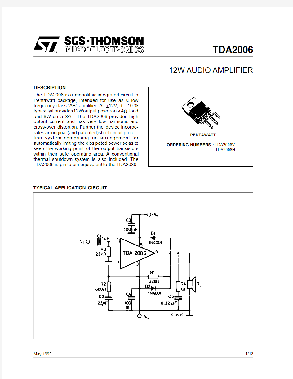
PENTAWATT ORDERING NUMBERS:TDA2006V
TDA2006H
DESCRIPTION
The TDA2006is a monolithic integrated circuit in
Pentawatt package,intended for use as a low
frequency class”AB”amplifier.At±12V,d=10%
typicallyit provides12Woutput poweron a4?load
and8W on a8?.The TDA2006provides high
output current and has very low harmonic and
cross-over distortion.Further the device incorpo-
rates an original(and patented)short circuit protec-
tion system comprising an arrangement for
automatically limiting the dissipated power so as to
keep the working point of the output transistors
within their safe operating area.A conventional
thermal shutdown system is also included.The
TDA2006is pin to pin equivalent to the TDA2030.
TYPICAL APPLICATION CIRCUIT
1/12
TDA2006
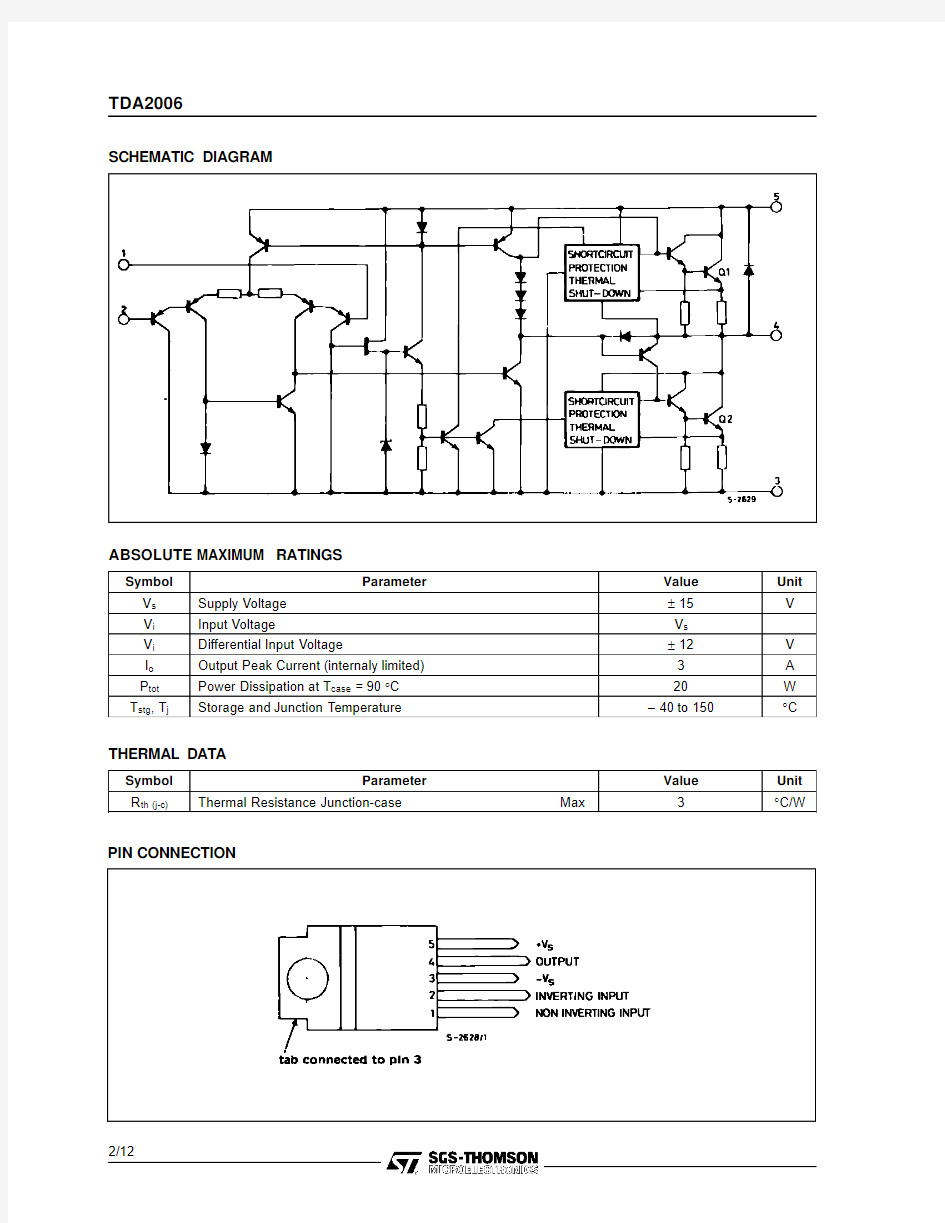
SCHEMATIC DIAGRAM
ABSOLUTE MAXIMUM RATINGS
Symbol Parameter Value Unit V s Supply Voltage±15V V i Input Voltage V s
V i Differential Input Voltage±12V
I o Output Peak Current(internaly limited)3A
P tot Power Dissipation at T case=90°C20W T stg,T j Storage and Junction Temperature–40to150°C
THERMAL DATA
Symbol Parameter Value Unit R th(j-c)Thermal Resistance Junction-case Max3°C/W
PIN CONNECTION
2/12
ELECTRICAL CHARACTERISTICS
(refer to the test circuit;V S=±12V,T amb=25o C unless otherwise specified)
Symbol Parameter Test Conditions Min.Typ.Max.Unit V s Supply Voltage±6±15V
I d Quiescent Drain Current V s=±15V4080mA
I b Input Bias Current V s=±15V0.23μA
V OS Input Offset Voltage V s=±15V±8mV
I OS Input Offset Current V s=±15V±80nA
V OS Output Offset Voltage V s=±15V±10±100mV
P o Output Power d=10%,f=1kHz
R L=4?
R L=8?612
8
W
d Distortion P o=0.1to8W,R L=4?,f=1kHz
P o=0.1to4W,R L=8?,f=1kHz 0.2
0.1
%
%
V i Input Sensitivity P o=10W,R L=4?,f=1kHz
P o=6W,R L=8?,f=1kHz 200
220
mV
mV
B Frequency Response(–3dB)P o=8W,R L=4?20Hz to100kHz
R i Input Resistance(pin1)f=1kHz0.55M?G v Voltage Gain(open loop)f=1kHz75dB G v Voltage Gain(closed loop)f=1kHz29.53030.5dB e N Input Noise Voltage B(–3dB)=22Hz to22kHz,R L=4?310μV i N Input Noise Current B(–3dB)=22Hz to22kHz,R L=4?80200pA SVR Supply Voltage Rejection R L=4?,R g=22k?,f ripple=100Hz(*)4050dB
I d Drain Current P o=12W,R L=4?
P o=8W,R L=8?850
500
mA
mA
T j Thermal Shutdown Junction
Temperature
145°C (*)Referring to Figure15,single supply.
TDA2006
3/12
TDA2006
Figure1:Output Power versus Supply Voltage Figure2:Distortion versus Output Power Figure3:Distortion versus Frequency Figure4:Distortion versus Frequency Figure5:Sensitivity versus Output Power Figure6:Sensitivity versus Output Power 4/12
Figure7:Frequency Response with different val-ues of the rolloff Capacitor C8(see
Figure13)Figure8:Value of C8versus Voltage Gain for dif-ferent Bandwidths(see Figure13)
Figure9:Quiescent Current versus
Supply Voltage Figure10:Supply Voltage Rejection versus
Voltage Gain
Figure11:Power Dissipation and Efficiency ver-sus Output Power Figure12:Maximum Power Dissipation versus
Supply Voltage
(sine wave operation)
TDA2006
5/12
TDA2006
Figure13:Application Circuit with Spilt Power Supply
Figure14:P.C.Board and Components Layout of the Circuit of Figure13(1:1scale) 6/12
TDA2006 Figure15:Application Circuit with Single Power Supply
Figure16:P.C.Board and Components Layout of the Circuit of Figure15(1:1scale)
7/12
Figure17:Bridge Amplifier Configuration with Split Power Supply(P O=24W,V S=±12V) PRACTICAL CONSIDERATIONS
Printed Circuit Board
The layout shown in Figure14should be adopted by the designers.If different layout are used,the ground points of input1and input2must be well decoupled from ground of the output on which a rather high current flows.
Assembly Suggestion
No electrical isolation is needed between the pack-age and the heat-sink with single supply voltage configuration.
Application Suggestion
The recommended values of the components are the ones shown on applicationcircuits of Figure13. Different values can be used.The table1can help the designers.
Table1
Component Recommanded
Value Purpose Larger Than
Recommanded Value
Smaller Than
Recommanded Value
R122k?Closed Loop Gain Setting Increase of Gain Decrease of Gain(*) R2680?Closed Loop Gain Setting Decrease of Gain(*)Increase of Gain
R322k?Non Inverting Input
Biasing Increase of Input
Impedance
Decrease of Input
Impedance
R41?Frequency Stability Danger of Oscillation at
High Frequencies with
Inductive Loads
R53R2Upper Frequency Cut-off Poor High Frequencies
Attenuation
Danger of Oscillation
C1 2.2μF Input DC Decoupling Increase of Low
Frequencies Cut-off
C222μF Inverting Input DC
Decoupling Increase of Low Frequencies Cut-off
C3C40.1μF Supply Voltage by Pass Danger of Oscillation C5C6100μF Supply Voltage by Pass Danger of Oscillation C70.22μF Frequency Stability Danger of Oscillation
C8
1
2πBR1Upper Frequency Cut-off Lower Bandwidth Larger Bandwidth
D1D21N4001To Protect the Device Against Output Voltage Spikes. (*)Closed loop gain must be higher than24dB.
TDA2006
8/12
SHORT CIRCUIT PROTECTION
Figure18:Maximum Output Current versus
Voltage V CE(sat)accross each Out-
put Transistor Figure19:Safe Operating Area and Collector
Characteristics of the Protected
Power Transistor
The TDA2006has an original circuit which limits the current of the output transistors.Figure18 shows that the maximum output current is a func-tion of the collector emitter voltage;hence the output transistors work within their safe operating area(Figure19).
This function can therefore be considered as being peak power limiting rather than simple current lim-iting.
It reduces the possibility that the device gets dam-aged during an accidental short circuit from AC output to ground.
THERMAL SHUT DOWN
The presence of a thermal limiting circuit offers the following advantages:
1)an overload on the output(even if it is
permanent),or an abo ve limit ambien t temperature can be easily supported since the T j cannot be higher than150°C.
2)the heatsink can have a smaller factor of safety
compared with that of a conventional circuit.
There is no possibility of device damage due to high junction temperature.
If for any reason,the junction temperature in-creases up to150°C,the thermal shutdown simply reduces the power dissipation and the current con-sumption.
The maximum allowable power dissipation de-pends upon the size of the external heatsink(i.e. its thermal resistance);Figure22shows the dissi-pable power as a function of ambient temperature for different thermal resistances.Figure20:Output Power and Drain Current ver-
sus Case Temlperature(R L=4?) Figure21:Output Power and Drain Current ver-
sus Case Temlperature(R L=8?)
TDA2006
9/12
Figure22:Maximum Allowable Power Dissipa-
tion versus Ambient Temperature DIMENSION SUGGESTION
The followingtable showsthe length of theheatsink in Figure23for several values of P tot and R th.
P tot(W)1286 Lenght of Heatsink(mm)604030
R th of Heatsink(°C/W) 4.2 6.28.3 Figure23:Example of Heatsink
TDA2006 10/12
L2L3
L5
L7
L6
Dia.
A
C
D
E
D 1
H 3
H 2
F
G
G 1
L1
L
M
M 1
F 1
PENTAWATT PACKAGE MECHANICAL DATA
DIM.mm inch MIN.
TYP.
MAX.MIN.
TYP.
MAX.A 4.80.189C 1.370.054D 2.4 2.80.0940.110D1 1.2 1.350.0470.053E 0.350.550.0140.022F 0.8 1.050.0310.041F11
1.4
0.0390.055G 3.40.1260.1340.142G1 6.8
0.2600.268
0.276H210.40.409H310.05
10.4
0.396
0.409
L 17.850.703L115.750.620L221.40.843L322.5
0.886
L5 2.630.1020.118L615.115.80.5940.622L76
6.6
0.236
0.260
M 4.50.177M14
0.157
Dia
3.65
3.85
0.144
0.152TDA2006
11/12
TDA2006
Information furnished is believed to be accurate and reliable.However,SGS-THOMSON Microelectronics assume s no responsibility for the consequences of use of such information nor for any infringement of patents or other rights of third parties which may result from its use.No license is granted by implication or otherwise under any patent or patent rights of SGS-THOMSON Microelectronics. Specifications mentioned in this publication are subject to change without notice.This publication supersedes and replaces all information previously supplied.SGS-THOMSON Microelectronics products are not authorized for use as critical components in life support devices or systems without express written approval of SGS-THOMSON Microelectronics.
?1995SGS-THOMSON Microelectronics-All Rights Reserved
PENTAWATT?is Registered Trademark of SGS-THOMSON Microelectronics
SGS-THOMSON Microelectronics GROUP OF COMPANIES
Australia-Brazil-France-Germany-Hong Kong-Italy-Japan-Korea-Malaysia-Malta-Morocco-The Netherlands-Singa-pore-Spain-Sweden-Switzerland-Taiwan-Thaliand-United Kingdom-U.S.A.
12/12
https://www.doczj.com/doc/8a5381645.html,
Copyright ? Each Manufacturing Company.
All Datasheets cannot be modified without permission.
This datasheet has been download from :
https://www.doczj.com/doc/8a5381645.html,
100% Free DataSheet Search Site.
Free Download.
No Register.
Fast Search System.
https://www.doczj.com/doc/8a5381645.html,