? Feature:
1. High brightness surface mount LED.
2. 120° viewing angle.
3. Small package outline.
4. Qualified according to JEDEC moisture sensitivity Level 2.
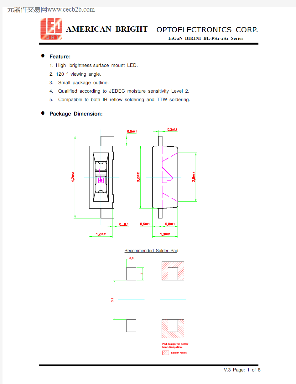
5. Compatible to both IR reflow soldering and TTW soldering. ? Package Dimension:
Recommended Solder Pad
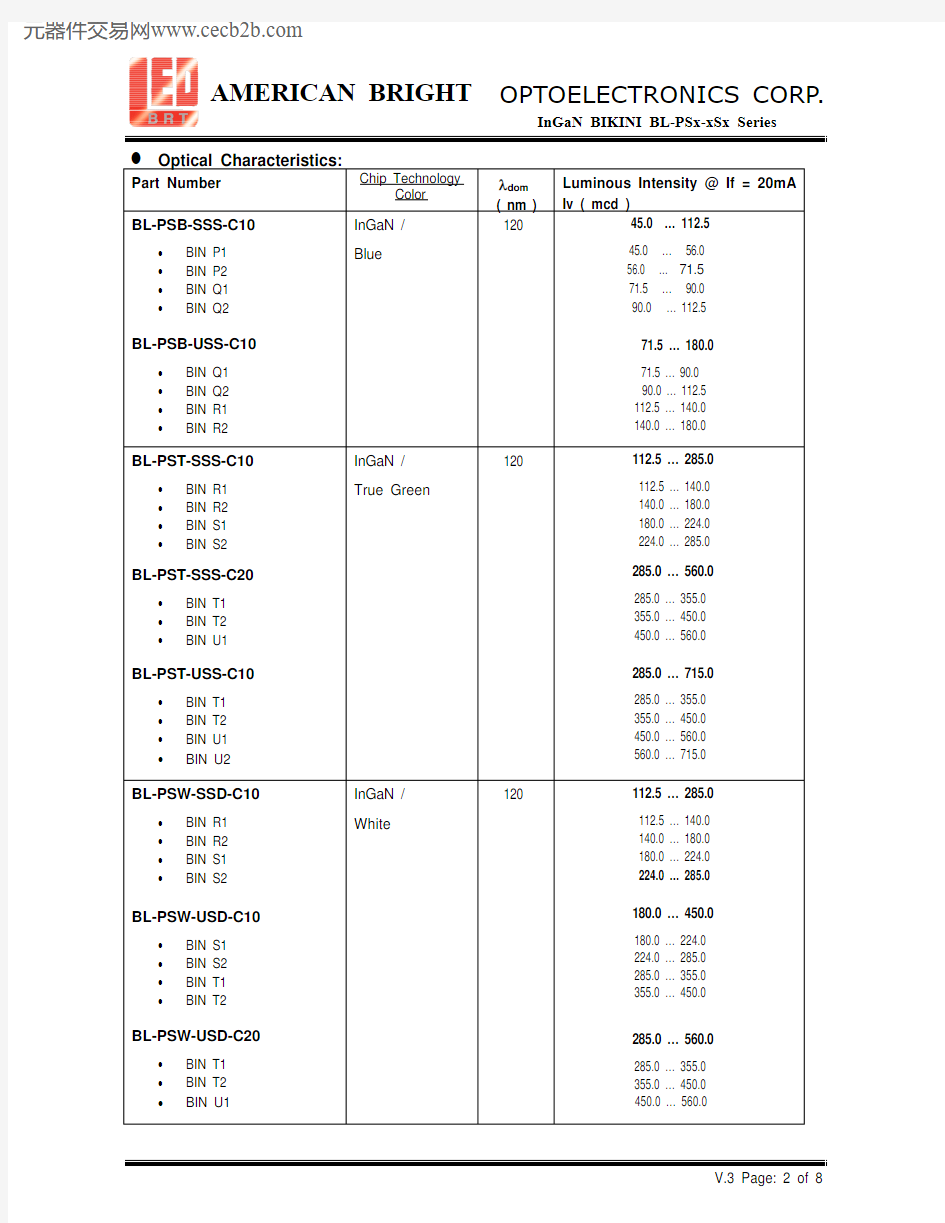
? Optical Characteristics:
Part Number Chip Technology
Color
λdom
( nm )
Luminous Intensity @ If = 20mA
Iv ( mcd )
BL-PSB-SSS-C10 ? BIN P1
? BIN P2
? BIN Q1
? BIN Q2
BL-PSB-USS-C10 ? BIN Q1
? BIN Q2
? BIN R1
? BIN R2 InGaN /
Blue
120 45.0 … 112.5
45.0 … 56.0
56.0 … 71.5
71.5 … 90.0
90.0 … 112.5
71.5 … 180.0
71.5 … 90.0
90.0 … 112.5
112.5 … 140.0
140.0 … 180.0
BL-PST-SSS-C10 ? BIN R1
? BIN R2
? BIN S1
? BIN S2
BL-PST-SSS-C20 ? BIN T1
? BIN T2
? BIN U1
BL-PST-USS-C10 ? BIN T1
? BIN T2
? BIN U1
? BIN U2InGaN /
True Green
120 112.5 … 285.0
112.5 … 140.0
140.0 … 180.0
180.0 … 224.0
224.0 … 285.0
285.0 … 560.0
285.0 … 355.0
355.0 … 450.0
450.0 … 560.0
285.0 … 715.0
285.0 … 355.0
355.0 … 450.0
450.0 … 560.0
560.0 … 715.0
BL-PSW-SSD-C10 ? BIN R1
? BIN R2
? BIN S1
? BIN S2
BL-PSW-USD-C10 ? BIN S1
? BIN S2
? BIN T1
? BIN T2
BL-PSW-USD-C20 ? BIN T1
? BIN T2
? BIN U1InGaN /
White
120 112.5 … 285.0
112.5 … 140.0
140.0 … 180.0
180.0 … 224.0
224.0 … 285.0
180.0 … 450.0
180.0 … 224.0
224.0 … 285.0
285.0 … 355.0
355.0 … 450.0
285.0 … 560.0
285.0 … 355.0
355.0 … 450.0
450.0 … 560.0
NOTE:
1. Luminous intensity is measured with an accuracy of ±11%.
2. Wavelength binning is carried for all units as per the wavelength-binning table. Only one wavelength group is
allowed for each reel.
3. Vf binning is available upon request. Binning scheme is as per following.
? Absolute Maximum Ratings:
Parameter Maximum Value Unit
DC forward current. 20 mA
200 mA
Peak pulse current.
(tp ≤ 10 μs, Duty cycle = 0.005)
Reverse voltage. 5 V
LED junction temperature. 125 °C
Operating temperature. -40 … +100 °C
Storage temperature. -40 … +100 °C
80 mW
Power dissipation
( at room temperature )
? Vf Binning:
Vf Bin @ 20mA Forward voltage (V)
Standard 3.05 … 4.25 (max)
00 3.05 … 3.35
01 3.35 … 3.65
02 3.65 … 3.95
03 3.95 … 4.25
Forward voltage, Vf is measured with an accuracy of ±0.1 V.
? Wavelength Grouping:
Color Group Wavelength distribution (nm)
BL-PSB; Blue Full
W
X
Y 464 - 476 464 - 468 468 - 472 472 - 476
BL-PST; True Green Full
W
X
Y
Z 520 - 536 520 - 524 524 - 528 528 - 532 532 - 536
Wavelength is measured with an accuracy of ±1 nm.
? BL-PSW: White Color Grouping
White bin coordinate
Chromaticity coordinate groups are measured with an accuracy of ±0.01.
Bin X Bin W
A1 Cx 0.2775 0.2900 0.29000.2775E1 Cx 0.32750.3400 0.3400 0.3275
Cy 0.2732 0.2939 0.31140.2907 Cy 0.35610.3768 0.3943 0.3736 A2 Cx 0.2775 0.2900 0.29000.2775E2 Cx 0.32750.3400 0.3400 0.3275
Cy 0.2557 0.2764 0.29390.2732 Cy 0.33860.3593 0.3768 0.3561 A3 Cx 0.2900 0.3025 0.30250.2900E3 Cx 0.34000.3525 0.3525 0.3400
Cy 0.2939 0.3146 0.33210.3114 Cy 0.37680.3975 0.4150 0.3943 A4 Cx 0.2900 0.3025 0.30250.2900E4 Cx 0.34000.3525 0.3525 0.3400
Cy 0.2764 0.2971 0.31460.2939 Cy 0.35930.3800 0.3975 0.3768 C1 Cx 0.3025 0.3150 0.31500.3025
Cy 0.3146 0.3354 0.35290.3321
C2 Cx 0.3025 0.3150 0.31500.3025
Cy 0.2971 0.3179 0.33540.3146
C3 Cx 0.3150 0.3275 0.32750.3150
Cy 0.3354 0.3561 0.37360.3529
C4 Cx 0.3150 0.3275 0.32750.3150
Cy 0.3179 0.3386 0.35610.3354
? Typical electro-optical characteristics curves:
Fig. 1 Relative luminous intensity vs. forward current. Fig. 2 Forward current vs. forward voltage.
Fig. 3 Radiation pattern.
Fig. 4 Maximum current vs. ambient temperature
Fig. 5 Relative Intensity vs. Wavelength
Fig. 6 Recommended IR-reflow Soldering Profile (acc. To IPC 9501).
Fig. 7 Recommended TTW Soldering Profile (acc. to CECC 00802).
? Taping And Orientation:
Reels come in quantity of 10,000 units or 2500 units.
Reel diameters are 330 mm and 180 mm respectively.