General Description
The MAX3967A is a programmable LED driver for fiber optic transmitters operating at data rates up to 270Mbps. The circuit contains a high-speed current dri-ver with programmable temperature coefficient (temp-co), adjustments for LED prebias voltage, and a disable feature. The circuit accepts PECL data inputs, and operates from a single +2.97V to +5.5V power supply.The SFP LED driver can switch up to 100mA into typical high-speed light-emitting diodes. As temperature increases, the device’s modulation current increases with a tempco that is programmable from 2500ppm/°C to 12,000ppm/°C. The modulation current is pro-grammed with a single external resistor.
The MAX3967A’s LED prebias voltage is programmable from 400mV to 925mV. The prebias circuit produces peaking current, which improves the LED switching speed.
Complementary current outputs help to maintain a con-stant supply current, reducing EMI and supply noise generated by the transmitter module. The MAX3967A is available in die form, or in a 4mm x 4mm, 24-pin thin QFN package.
Applications
Multimode LED Transmitters
Fast Ethernet/FDDI
155Mbps LAN ATM Transceivers ESCON Receivers SFP Transceivers
Features
?TX_DISABLE for SFP Compatibility ?Single +2.97V to +5.5V Power Supply ?Adjustable Temperature Compensation ?Adjustable Modulation Current
?Complementary Output Reduces Supply Noise ?Programmable LED Prebias Voltage ?Available in 24-Pin Thin QFN or Die
MAX3967A
270Mbps SFP LED Driver
________________________________________________________________Maxim Integrated Products
1
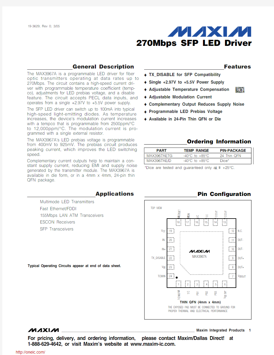
Pin Configuration
19-3629; Rev 0; 3/05
For pricing, delivery, and ordering information,please contact Maxim/Dallas Direct!at 1-888-629-4642, or visit Maxim’s website at https://www.doczj.com/doc/827160844.html,.
Ordering Information
Typical Operating Circuits appear at end of data sheet.
*Dice are tested and guaranteed only at T A = +25°C.
M A X 3967A
270Mbps SFP LED Driver 2_______________________________________________________________________________________
ABSOLUTE MAXIMUM RATINGS
Supply Voltage at V CC , V CCOUT
(V EE , V EEOUT = 0V)..............................................-0.5V to +7V Current into OUT+, OUT-................................-40mA to +160mA Differential Output Voltage (OUT+ to OUT-).........-3.3V to +3.3V Voltage at PB1, PB2, PB3,
IN+, IN-, OUT+, OUT-, TX_DISABLE......-0.5V to (V CC + 0.5V)Voltage at TCMIN, TCNOM, TC, MODSET, MON ....-0.5V to +2V
Continuous Power Dissipation (T A = +85°C)24-Lead Thin QFN (derate 20.8mW/C °
above +85°C).............................................................1354mW Operating Junction Temperature Range...........-40°C to +150°C Die Attach Temperature...................................................+375°C Storage Temperature Range.............................-50°C to +150°C Lead Temperature (soldering, 10s).................................+300°C
Stresses beyond those listed under “Absolute Maximum Ratings” may cause permanent damage to the device. These are stress ratings only, and functional operation of the device at these or any other conditions beyond those indicated in the operational sections of the specifications is not implied. Exposure to absolute maximum rating conditions for extended periods may affect device reliability.
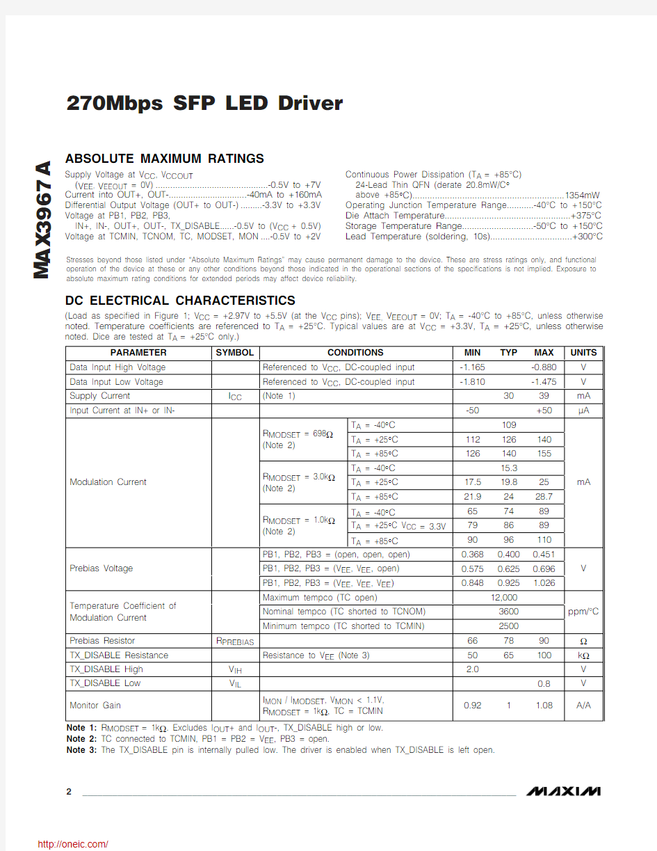
DC ELECTRICAL CHARACTERISTICS
(Load as specified in Figure 1; V CC = +2.97V to +5.5V (at the V CC pins); V EE , V EEOUT = 0V; T A = -40°C to +85°C, unless otherwise noted. Temperature coefficients are referenced to T A = +25°C. Typical values are at V CC = +3.3V, T A = +25°C, unless otherwise noted. Dice are tested at T A = +25°C only.)
EE Note 3:The TX_DISABLE pin is internally pulled low. The driver is enabled when TX_DISABLE is left open.
MAX3967A
270Mbps SFP LED Driver
_______________________________________________________________________________________3
AC ELECTRICAL CHARACTERISTICS
(Load as specified in Figure 1, unless otherwise noted. V CC = +2.97V to +5.5V (at the V CC pins), R MODSET = 1k ?, T A = -40°C to +85°C. Input data shaped by 470MHz 4-pole filter, PB1 = PB2 = V EE , PB3 = open. Typical values are at V CC = +3.3V, TC connected
Figure 1. MAX3967A Output Test Loads
CURRENT ON CURRENT OFF Note 6:Test pattern is a K28.5 (0011 1110 1011 0000 0101) transmitted at 266Mbps.
Note 7:Test pattern is equivalent to a 213- 1 PRBS containing 72 consecutive zeros or 72 consecutive ones.
M A X 3967A
270Mbps SFP LED Driver 4
_______________________________________________________________________________________
Typical Operating Characteristics
(MAX3967AETG in Maxim evaluation board, V CC = +3.3V, PB1 = PB2 = V EE , PB3 = open, TC connected to TCNOM, R MODSET =1k ?, T A = +25°C, unless otherwise noted.)
4038363432302826242220
-40-20-10-300102030405060708090
SUPPLY CURRENT vs. TEMPERATURE
AMBIENT TEMPERATURE (°C)
S U P P L Y C U R R E N T (m A )
40
208060100120
-402040-2006080
MODULATION CURRENT vs. TEMPERATURE
AMBIENT TEMPERATURE (°C)
M O D U L A T I O N C U R R E N T (m A )
40208060
1001200608020
40100120
140
DIE MODULATION CURRENT
vs. TEMPERATURE
JUNCTION TEMPERATURE (°C)
M O D U L A T I O N C U R R E N T (m A )
100,0001000
1
10100
MODULATION CURRENT TEMPCO
vs. R TC
R TC (k ?)
M O D U L A T I O N C U R R E N T T E M P C O (p p m /°C )
10,000
200
10500
1k
10k
MODULATION CURRENT
vs. R MODSET
R MODSET (?)
M O D U L A T I O N C U R R E N T (m A )
100
200
10500
1k
8k
DIE MODULATION CURRENT
vs. R MODSET
R MODSET (?)
M O D U L A T I O N C U R R E N T (m A )
100
EYE DIAGRAM (ELECTRICAL)
266Mbps
MAX3967 toc07
500ps/div
PATTERN = 231
- 1 PRBS
EYE DIAGRAM (OPTICAL)
155Mbps
MAX3967 toc08
1ns/div
RECEIVER BW = 200MHz, V CC = 2.97V, T A = +85°C, P AVE = -17.1dBm, PATTERN = 231 - 1 PRBS
EYE DIAGRAM (OPTICAL)
155Mbps
MAX3967 toc09
1ns/div
RECEIVER BW = 200MHz, V CC = 5.5V, T A = -40°C, P AVE = -15.8dBm, PATTERN = 231 - 1 PRBS
MAX3967A
270Mbps SFP LED Driver
_______________________________________________________________________________________
5
EYE DIAGRAM (OPTICAL)
155Mbps
MAX3967 toc10
1ns/div
RECEIVER BW = 200MHz, V CC = 5.5V, T A = +85°C, P AVE = -17.1dBm, PATTERN = 2
31 - 1 PRBS
EYE DIAGRAM (OPTICAL)
155Mbps
MAX3967 toc11
1ns/div
RECEIVER BW = 200MHz, V CC = 2.97V, T A = -40°C, P AVE = -15.8dBm, PATTERN = 231 - 1 PRBS
02143560
10
20
30
40
50
60
70
8090
RANDOM JITTER vs. TEMPERATURE
AMBIENT TEMPERATURE (°
C)
R A
N D O M J I T T E R (p s
R M S )
TX_DISABLE NEGATE TIME
4ns/div LED OUTPUT TX_DISABLE
TX_DISABLE ASSERT TIME
4ns/div
LED OUTPUT
TX_DISABLE
Typical Operating Characteristics (continued)
(MAX3967AETG in Maxim evaluation board, V CC = +3.3V, PB1 = PB2 = V EE , PB3 = open, TC connected to TCNOM, R MODSET =1k ?, T A = +25°C, unless otherwise noted.)
M A X 3967A
Detailed Description
The MAX3967A provides a flexible current drive for the modulation of fiber optic light-emitting diodes (LEDs).The circuit is designed to be used with +3.3V or +5V power supplies. The IC provides up to 100mA of modu-lation current. An adjustable prebias current source sets the LED prebias voltage. An integrated resistor provides passive peaking and optical pulse-width compensation.F igure 2shows a block diagram of the MAX3967A,which comprises a reference-voltage generator, modu-lation-current generator, input buffer with disable, pre-bias-current generator, main output driver,complementary output driver, and LED-compensation network.
Temperature Compensation
The reference-voltage generator circuit provides two voltage sources that create modulation-current tempera-ture compensation. A positive modulation-current tem-perature coefficient (tempco) is useful to compensate for the temperature characteristics of typical fiber optic LEDs. The first source has a temperature-stable output.The second source has a temperature-increasing output with a tempco of approximately 12,000ppm/°C (relative to +25°C). A resistor-divider between the two reference generators programs the modulation-current tempco.For maximum modulation-current tempco, leave the TC pin disconnected. F or a tempco of approximately 3600ppm/°C, connect TC to TCNOM. To obtain the mini-mum tempco, connect TCMIN to TC. Intermediate temp-co values can be programmed by connecting an external resistor (R TC ) between TCMIN and TC.
Input Buffer
The inputs are connected to the PECL-compatible differ-ential input buffer. If left unconnected, IN+ is internally pulled to a PECL low and IN- is pulled to a PECL high,causing low current at OUT+. The input impedance of IN+ and IN- is approximately 50k ?.
270Mbps SFP LED Driver 6
_______________________________________________________________________________________
Modulation-Current Generator
The modulation-current generator circuit provides con-trol of the modulation-current amplitude. This amplitude is determined by the voltage at the MODSET pin and external resistor R MODSET.
Do not connect bypass capacitors at the MODSET pin.Capacitance at this pin increases high-frequency out-put noise. The MON pin provides an optional modula-tion-current monitor. The current sourced from the MON pin is 1/96 of the modulation current. If used, the pin should be connected to V EE through a resistor. The resistance must be chosen so the voltage on MON does not exceed 1.1V. If not used, leave MON open.
Prebias Current Generator
A prebias voltage (V PREBIAS ) can be applied to the LED to improve switching speed. The prebias current generator creates a current that flows through the 78?prebias resistor in the output stage, creating a prebias voltage. The prebias voltage can be adjusted by selec-tively connecting pins PB1, PB2, and PB3 to V EE . Table 1describes the functions of PB1, PB2, and PB3.
Output Current Drivers
The modulation-current reference is switched and amplified by the output stages.
LED package lead inductance causes ringing and overshoot, which can be compensated with an RC filter network. The MAX3967A includes 35?and 12pF of
MAX3967A
270Mbps SFP LED Driver
_______________________________________________________________________________________
7
Figure 2. Functional Diagram
M A X 3967A
internal compensation. The compensation network can be optimized by adding additional components between V CCOUT and OUT+.
The MAX3967A includes a complementary output dri-ver, which is switched 180°out of phase with the main output. This configuration helps to maintain constant current flow from the voltage supply, reducing noise and EMI. A large diode and a 5?resistor are connect-ed in series with the negative output (OUT-) to emulate the LED load at OUT+.
Peaking Current
The prebias resistor provides peaking current to improve the LED switching speed. The peaking magnitude is given by the following equation:
The peaking amplitude is equal for rising and falling data transitions.
Design Procedure
Select an LED
F or best performance, select a high-efficiency, low-inductance LED. LED inductance causes large voltage swings and ringing.
Program the Modulation-Current Tempco
Select a modulation-current tempco that provides near-ly constant LED output power as temperature varies.For the minimum tempco, connect TCMIN to the TC pin.F or a tempco of approximately 3600ppm/°C, connect TC to TCNOM and leave TCMIN unconnected. For the maximum tempco, leave TCMIN, TCNOM, and TC unconnected.
See the Modulation Current Tempco vs. R TC graph in the Typical Operating Characteristics to program a cus-tom tempco. From the graph, determine the appropriate resistor and connect it between TCMIN and TC.
For example, if an LED requires a 5000ppm/°C tempco,choose R TC of 8.3k ?.
Program the Modulation Current
Determine the required modulation current at T A = +25°C.Then select the appropriate value of R MODSET from the Modulation Current vs. R MODSET graph in the Typical Operating Characteristics .
For example, to program 75mA modulation current, the graph indicates an R MODSET value of 750?for maxi-mum tempco (12,000ppm/°C) and 1k ?for nominal tempco (3600ppm/°C). By interpolation, choose an R MODSET of 792?for a tempco of 5000ppm/°C.
Program Prebias Voltage
Determine the LED prebias voltage that produces an acceptable trade-off between peaking current and extinc-tion ratio. See Table 1for PB1, PB2, and PB3 settings.
Layout Considerations
For optimum performance, total load inductance should not exceed 10nH. Load inductance includes LED inductance, LED package lead inductance, and circuit-board traces. Keep the connections between the MAX3967A OUT pins and the LED as short as possible to minimize inductance.
Chip-and-wire (hybrid) technology reduces package inductance significantly, and provides the best possible performance.
Use good high-frequency layout techniques and a multilayer board with an uninterrupted ground plane.Power supplies should be capacitively bypassed to the ground plane with surface-mount capacitors located near the power-supply pins.
I PEAK LED PREBIAS
V -V
78=?
270Mbps SFP LED Driver 8_______________________________________________________________________________________
Applications Information
Wire-Bonding Die
The MAX3967A utilizes gold metalization, which pro-vides high reliability. Make connections to the die with gold wire only, using ball-bonding techniques. Use caution if attempting wedge-bonding. Pad size is 4 mils x 4 mils (100μm). Die thickness is typically 15 mils (375μm).
Exposed-Pad Package
The exposed pad on the 24-pin TQFN provides a very low thermal resistance path for heat removal from the IC.
Chip Information
TRANSISTOR COUNT: 331
SUBSTRATE CONNECTED TO V EE PROCESS: BIPOLAR DIE THICKNESS: 15 mils
MAX3967A
270Mbps SFP LED Driver
_______________________________________________________________________________________9
Figure 3. Input Terminations
M A X 3967A
270Mbps SFP LED Driver
Typical Operating Circuits
分销商库存信息:
MAXIM
MAX3967AETG+MAX3967AETG+T