Developing a PWM Interface using LabVIEW FPGA
- 格式:pdf
- 大小:111.77 KB
- 文档页数:5
用C 语言和M A TLAB 构造PWM 控制仿真模型的一种方法华中理工大学 董玮 秦忆 摘要:文章介绍了一种将C 语言与M A TLAB 结合起来进行构造PWM 仿真模型的方法,这种方法不用编程,简单直观,使用方便,易于模块化。
关键词:PWM 控制 M A TLAB S I M UL I N KA Si m ula tion M ethod to P WM Con trol with C and M AT LABDong W ei Q in Y iAbstract :A m ethod to construct PWM si m ulati on model w ith C and M A TLAB has been introduced in the paper .T he m ethod is si m p le and intuiti onal w ithout any p rogram .It is convenient to use and m ake modulariza 2ti on .Keywords :PWM contro l M A TLAB S I M UL I N K1 前言PWM 控制是通过对每周期内输出脉冲个数和每个脉冲宽度的控制来改善逆变器的输出电压、电流波形[1]。
它是现代交流变频调速的一种重要的控制方式。
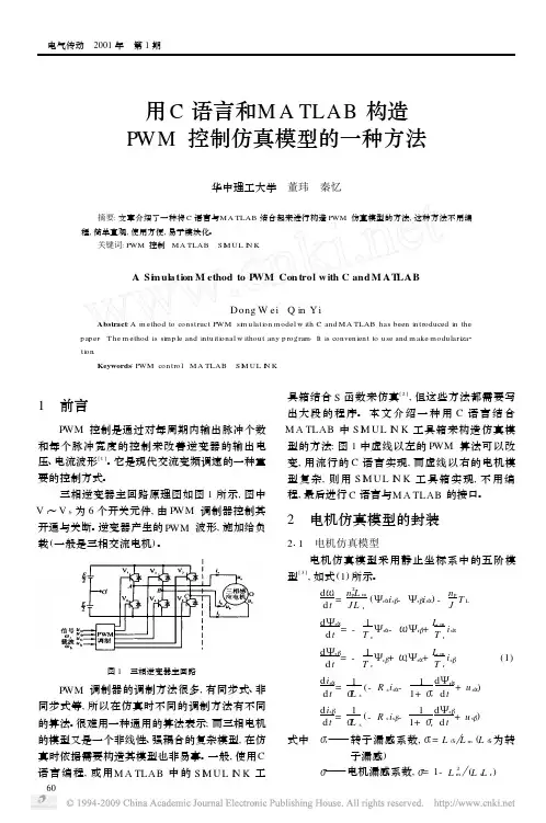
三相逆变器主回路原理图如图1所示,图中V 1~V 6为6个开关元件,由PWM 调制器控制其开通与关断。
逆变器产生的PWM 波形,施加给负载(一般是三相交流电机)。
图1 三相逆变器主回路PWM 调制器的调制方法很多,有同步式、非同步式等,所以在仿真时不同的调制方法有不同的算法。
很难用一种通用的算法表示;而三相电机的模型又是一个非线性、强耦合的复杂模型,在仿真时依据需要构造其模型也非易事。
一般,使用C 语言编程,或用M A TLAB 中的S I M UL I N K 工具箱结合S 函数来仿真[2],但这些方法都需要写出大段的程序。

华为突破技术封锁自主研发芯片英语作文Huawei Breaks Through Technology Blockade withSelf-developed ChipsWith the advancement of technology and the increasing competition in the global market, the issue of technological blockade has become more prominent. In recent years, Huawei, a leading global provider of information and communications technology (ICT) infrastructure and smart devices, has continuously faced technological challenges and restrictions. However, Huawei has successfully broken through the technology blockade by developing its own chips.In the face of the technology blockade, Huawei has invested heavily in research and development to develop its own chips. The company has established a strong research and development team comprised of experts in various fields, including chip design, semiconductor technology, and artificial intelligence. Through their collaborative efforts, Huawei has successfully developed a series of cutting-edge chips that have not only improved the performance of its products but also reduced its dependence on foreign suppliers.One of the key achievements of Huawei in breaking through the technology blockade is the development of its Kirin series of chips. The Kirin chips are designed to provide superior performance, energy efficiency, and security for Huawei's smartphones, tablets, and other devices. By using its own chips, Huawei has been able to optimize the performance of its devices and deliver a better user experience to its customers.In addition to the Kirin chips, Huawei has also developed its own Kunpeng and Ascend series of chips for its server and artificial intelligence products. The Kunpeng chips are designed to provide high-performance computing capabilities for Huawei's server products, while the Ascend chips are designed to provide advanced AI processing capabilities for Huawei's AI products. By developing its own chips, Huawei has been able to expand its product offerings and compete more effectively in the global market.Overall, Huawei's success in breaking through the technology blockade with its self-developed chips is a testament to the company's innovation and determination. By investing in research and development and fostering a culture of continuous improvement, Huawei has been able to overcome the technological challenges it faces and emerge as a global leaderin the ICT industry. As Huawei continues to develop new technologies and products, it is poised to further strengthen its position in the global market and drive innovation in the ICT industry.。
3B SCIENTIFIC ®PHYSICS1Light barrier U11365Instruction sheet01/10 Hh/5700121. Safety instructions•When using the equipment in conjunction with a laser source, strictly observe the stipulated safety regulations.•Never look directly into the laser beam.2. Scope of delivery1 Light barrier1 Stand rod, length: 120 mm1 8-pin mini DIN connection cable, length: 1 m 1 Knurled screw M6x13. DescriptionThe light barrier can be used in two operating modes.1. Internal light barrier mode: light barrier with an infrared light source and an infra-red detector with a very short signal delay for measuring time inter-vals with moving bodies, e.g. during free fall, in airtrack experiments and for pendulum oscillations, as well as for counting pulses.2. Laser light barrier mode: laser diode detector built in at the side for setting up a wide-range barrier along with a laser pointer, e.g. during sport-ing events.The light barrier is equipped with a built-in LED function display: beam broken = 1 (TTL high). When disabled or when the beam is interrupted, the LED function display comes on.The narrow barrier arm in front of the infra-red source includes a sliding mechanical shutter that is used for disabling internal light-barrier mode and activating laser light -barrier mode.4. Technical dataSeparation of prongs: 82 mm Rise time: 60 ns Spatial resolution: < 1 mm Time resolution:10 µs3B Scientific GmbH • Rudorffweg 8 • 21031 Hamburg • Germany • Subject to technical amendments© Copyright 2010 3B Scientific GmbH5. Operation•Screw onto the stand rod using the arm at-tached to the thinner of the two prongs of the barrier and the M6 nut provided for this pur-pose.•Insert the mini DIN cable into the mini DIN connector on the broader prong of the barrier and connect it to the 3B NET log TM interface U11300 or to digital counter U210051.•Activate internal light barrier mode by opening the mechanical shutter. Subsequently, mount and focus the device for the intended applica-tion.•Activate laser light barrier mode by closing the mechanical shutter and (roughly) focus the la-ser light source onto the opening at the side of the light barrier. To achieve this, mirrors may be used to deflect the laser beam. Make fine adjustments to the light barrier.6. ApplicationsDetermining the position, velocity and acceleration of moving bodiesDetermining the acceleration due to gravity g in free fall experimentsMeasuring periods of oscillating bodies7. Sample experimentDetermining acceleration due to gravity g using picket fence U11366 Required apparatus:1 3B NET log TMU11300 1 Light barrier U11365 1 Picket fence U11366 1 Stand base U13270 1 Steel rod, length: 750 mm U15003 1 Universal clamp U13255 (1 Foam rubber sheet, approx. 20 x 20 cm)• Use the stand apparatus to fix the light barrierat a suitable height above ground level or at the edge of a table. If necessary, place a cush-ioning surface (e.g. foam rubber sheet) along the point of impact.• Select the digital input of the 3B NET log TMinter-face and load the free-fall experiment (tem-plate) from the 3B NET labTM software. All thenecessary settings required for evaluation are provided by this software.•Conduct the experiment and analyse yourresults.Fig. 1: Measuring free fallFig. 2: Distance against timeFig. 3: Fall velocity against time。
Evaluates: MAX20754 and MAX20790MAX20754EVKIT8Evaluation KitOne Analog Way, Wilmington, MA 01887 U.S.A. | Tel: 781.329.4700 | © 2021 Analog Devices, Inc. All rights reserved.© 2021 Analog Devices, Inc. All rights reserved. Trademarks and registered trademarks are the property of their respective owners.Click here to ask an associate for production status of specific part numbers.General DescriptionThis MAX20754EVKIT8 evaluation kit (EV kit) demon-strates the MAX20754 PMBus™-compatible dual-output multiphase power-supply controller. The controller gener-ates six pulse-width modulated (PWM) control signals, or “phases.” The MAX20754EVKIT8 EV kit is a single-output design, with all six phases assigned to one output. The output uses coupled inductor topologies. Coupled induc-tors reduce the effective inductor value and size without excessive ripple current, reducing required output capaci-tance, and improving transient response.The EV kit also demonstrates the MAX20790 power-stage device; there are six MAX20790 devices, one per phase.Features●Optimized for Single +10V to +16V Supply• Onboard +3.3V Regulator (MAX17501) ●Generates One Output• Output: 6-Phase, 1V, 225A ●500kHz Switching Frequency ●Enable Switch●PMBus Configuration and Control• Compatible with Maxim’s PowerTool™ GUI • Easy Connection to PC Using MAXPOW-ERTOOL002 USB-to-SMBus Interface (order separately) ●Status LEDs• Power-Good• Power-Stage Fault • SMBus Alert ●Proven PCB Layout●Compensation Scheme Optimized for HighBandwidth ●Fully Tested and Assembled319-100863; Rev 0; 12/21Ordering Information appears at end of data sheet.PMBus is a trademark of SMIF , Inc.PowerTool is a trademark of Maxim Integrated Products, Inc.MAX20754EVKIT8 BoardEvaluation KitQuick StartRequired Equipment●12V DC power supply capable of delivering 300W atthe desired input voltage●Windows PC with a spare USB port●MAXPOWERTOOL002 USB-to-SMBus Interface(order separately)●Maxim Digital PowerTool GUI softwareOptional Equipment●AC/DC “wall adapter” for convenient low-power eval-uation, connecting to J5 on the EV kit. For example:• CUI p/n ETSA120500UC-P5P-SZ (12V, 5A, 60Wmax)• CUI p/n EMSA120300-P5P-SZ (12V, 3A, 40W max)●300MHz four-channel oscilloscope●BNC-to-SMB cables for convenient, low-noise oscil-loscope connection to the input and output voltagesense points. For example: CD International Tech-nology p/n BSB-174TPR-3.●Electronic load capable of sinking 240A at 1V• Ask about the Maxim MINILOAD device●Digital multimeter (DMM)ProcedureNote: In the following sections, text in bold refers to items directly from the EV kit software.The EV kit is fully assembled and tested. Follow the steps below to verify board operation.Caution: Do not turn on the power supply until all connections are completed.1) Visit the Maxim Integrated website to download andinstall the latest version of the Digital PowerToolsoftware.2) Connect the USB cable from the PC to the MAX-POWERTOOL002 interface adapter.3) Connect the adapter ribbon cable to the matchingheader J13 on the EV kit, ensuring that J13-Pin 1 isadjacent to the red wire on the ribbon cable.4) Connect the DC power supply positive lead to J6 andthe negative lead to J7 (or use an AC-DC adapterthrough J5 using a center-positive 2.1mm I.D. x5.5mm O.D. plug).5) If available, connect the electronic load(s) to theoutputs at screw terminals ST1, ST2, ST3, and ST4, being careful to observe the VOUT and GND polarity indicated by the silkscreen labels.6) If available, connect the oscilloscope to the EV kit forwaveform analysis. Coaxial SMB cable connections J8, and J9 allow low-noise measurement of the input and output ripple waveforms. (Note that the inputvoltage signal at J8 is resistively attenuated 20:1 toprotect oscilloscope inputs.)7) Ensure that jumpers JP1 and JP2 have shuntsinstalled.8) Enable the external 12V supply.9) Enable the onboard MAX17501 12V-to-3.3V sup-ply circuit with switch S5. This supplies 3.3V to theMAX20754, which in turn generates 1.8V power forthe MAX20790 power-stage devices.10) Start the GUI software. The “Dashboard” windowshould appear as shown in Figure 1.11) Enable the MAX20754 output by operating switch S2on the EV kit, or by setting the OPERATION and ON_ OFF_CONFIG commands in the PowerT ool GUI.Evaluation KitDetailed Description of SoftwareThe PowerT ool software presents system-level information on the Dashboard tab. This view collects basic information for all Maxim PMBus devices found on the bus. This tab configures sequencing and output voltage levels and pres-ents an overview of the system status. Clicking the Stop Communication button stops all PMBus transactions from the PowerT ool GUI. T o force detection of all active devices on the bus, click the Search for Devices button.For detailed information on a particular device, click on the sub-tab for that device’s slave address. This opens a view with a set of further sub-tabs specific to that device as shown in Figure 2. The sub-tabs available vary depending on the GUI version and the connected device’s capability, but typically include Configuration, Monitor, Faults Set, and PMBus Command.The Configuration tab presents the most commonly used PMBus command data in human-readable form. The device status is updated by continuous polling of these commands. Configuration settings for an individual device can be saved to or restored from an external file. The PMBus command settings can be saved to or restored from the device’s internal nonvolatile memory as well.The Monitor tab shows continuously updated telemetry data from the device. Rolling plots of output voltage, input voltage, output current, and temperature data are shown, including indication of fault limits relative to the operating point.Figure 1. Maxim PowerTool Graphical User Interface Software Dashboard WindowEvaluation KitThe Faults Set tab allows the user to configure andmonitor the status of most protection and warning func-tions. The fault levels and fault response commands areconfigured from this tab. The full contents of the STATUS_register commands are available by clicking the ViewFault/Warning bit by bit button. Fault and warning flags are cleared by clicking the Clear Fault/Warning button,which sends the CLEAR_FAULTS PMBus command tothe device.The PMBus Command tab shows all supported PMBus commands in a series of sub-tabs, allowing detailed con-figuration and analysis of the command values. The user can view the command values in a hexadecimal or deci-mal format by checking or clearing the Force Hex check-box. The Use PEC checkbox enables or disables Packet Error Checking for all GUI communications. Note that the command data is continuously updated by polling; typing a new value into the text boxes causes the new value to be sent to the device.Figure 2. Detailed View for One Device; Configuration Sub-TabEvaluation KitDetailed Description of HardwareThe MAX20754EVKIT8 demonstrates a single-output step-down power supply solution, with one six-phase output, which makes use of the coupled inductors. This solution provides high output-current with high efficiency, fast load-transient response, and low ripple and noise.The MAX20754 controller automatically interleaves all PWM outputs assigned to a given output at even inter-vals. The output is six-phase resulting in 60° timing. Each PWM signal is connected to one MAX20790 power-stage device, operating in parallel configuration. This configura -tion is capable of supplying up to 37.5A per phase. Each power-stage is in turn connected to one winding of a coupled inductor.The MAX20754 controller evenly shares the load current between phases in a given output. The EV kit is con-figured to operate both outputs at 500kHz fundamental switching frequency, but can be modified to operate anywhere from 300kHz to 800kHz with appropriate com -pensation network changes. The output is set to supply 1V. The maximum output current for the output is 225A.The output voltage, output rise-time and fall-time, switch -ing frequency, PMBus address, slope compensation, and maximum output current are set using only five external resistors, allowing simple setup and application configura -tion that does not require PMBus commands. Refer to the MAX20754 and MAX20790 integrated circuit data sheets for complete details on design and component selection.Table 1. Jumper JP1Table 2. Jumper JP2Table 3. Connector ListSHUNT POSITIONDESCRIPTIONInstalled MAX17501 +3.3V output connected to MAX20754 V DD3P3 input.Not installedMAX20754 can be powered by an external +3.3V supply at TP35.SHUNT POSITIONDESCRIPTIONInstalled MAX17501 +3.3V output connected to AUX3P3 rail (ENx debounce and status LED logic, etc.).Not installedThe AUX3P3 rail can be powered by an external +3.3V supply at Pin 2 of JP2.REFERENCE DESIGNATORDESCRIPTIONJ6Input supply positive voltage (+5V to +16V)J7Input supply groundST1Rail 1 output positive voltage ST2Rail 1 output ground ST3Rail 1 output positive voltage ST4Rail 1 output groundJ13Header for connection to MAXPOWERTOOL002 USB-to-SMBus interface.Pin 1: SCL Pin 3: SDA Pin 7: ALERTEven-numbered pins: GroundJ8SMB jack for input supply monitoring. This connection has a 1/20 resistive divider with 50Ω back-impedance. Connect to an oscilloscope with 20x scaling and ≥1MΩ input resistance.J9SMB jack for Rail 1 output voltage monitoring. This connection has 50Ω back-impedance. Connect to an oscilloscope with 1x scaling and ≥1MΩ input resistance.J5Alternate input supply barrel connector, 2.1mm I.D. x 5.5mm O.D. barrel jack, center-positive. Do not exceed 5A current.Evaluation KitTable 4. SwitchesTable 5. Test PointsREFERENCE DESIGNATORFUNCTIONS5SPDT toggle switch. Enable MAX17501 +3.3V buck regulator to supply V DD3P3Green light: output enabledS4Momentary tactile switch; no function on MAX20754S2SPDT toggle switch. Enable Rail 1 output regulation.Green light: PGOOD1 pin highAmber light: ALERT pin asserted lowRed light: FAULT pin asserted low (power stage fault detected)REFERENCE DESIGNATORDESCRIPTIONTP21ALERT signal (open-drain)TP20FAULT signal (open-drain)TP36SDA signal (open-drain)TP37SCL signal (open-drain)TP17EN1 signal (open-drain)TP7Input supply positive voltage TP8Input supply groundTP19Input voltage sense point for efficiency measurements TP22Input ground sense point for efficiency measurements TP18PGOOD1 signal (open-drain)TP6PWM0 signal (Rail 1)TP5PWM1 signal (Rail 1)TP4PWM2 signal (Rail 1)TP3PWM3 signal (Rail 1)TP2PWM4 signal (Rail 1)TP1PWM5 signal (Rail 1)TP13Rail 1 loop-response (Bode plot) measurement positive injection point (see MAX20754 EV Kit Schematic )TP23Rail 1 loop-response (Bode plot) measurement negative injection point (see MAX20754 EV Kit Schematic )TP25Rail 1 output voltage efficiency measurement point TP26Rail 1 output ground efficiency measurement pointTP9Rail 1 output voltage feedback sense point (for line/load regulation accuracy measurement with DMM)TP10Rail 1 output ground feedback sense point (for line/load regulation accuracy measurement with DMM)TP34V DDS supply; +1.8V power to MAX20790 power stage, from MAX20754 integrated switcher output TP35V DD3P3 supply; +3.3V power to MAX20754 integrated switcher TP29, TP30, TP31, TP32,TP33, TP39GroundEvaluation Kit#Denotes RoHS compliance.PARTTYPE MAX20754EVKIT8#MAX20754 EV Kit MAXPOWERTOOL002#USB-to-SMBus Interface5.0mV/div(AC-COUPLED)V OUT(V = 1V, I = 0A, f = 500kHz)PHASE MARGIN = 62.24BANDWIDTH = 68.75kHz50mV/div(AC-COUPLED)50A/divOrdering InformationEvaluation KitMAX20754 EV Kit Bill of MaterialsEvaluation KitMAX20754 EV Kit Bill of Materials (continued)0 0Evaluation KitMAX20754 EV Kit SchematicP W M 2R A T I O = 0.068238 T O M A T C H V I N _S C A L E _M O N I T O R D E F A U L TN O D R O O PR I N TZ 12 2 16 2 5 4 13 0 <----P H A S E S F I R I N G O R D E R 1 2P W M 5P W M 0O U T P U T #1V O U T 1:R 1R D E SZ 25 2 4 1 3 04 2 4 1 33 2 1 3R L DP W M 3P W M 1P W M 4O U T P U T #1C O M P E N S A T I O N N E T W O R K S C H E M E 9AC 2R 2C L DC I N TT O N _R I S E , T O F F _F A L L : 0.5M SO C P = 257AA D D R E S S : 0X 5A M R A M P : M H (0X 25, 37 D E C .)F R E Q U E N C Y _S W I T C H : 500K H Z V O U T _C O M M A N D : 1.0V T P 33T P 30T P 29T P 23T P 13T P 34R 58R 47R 21R 38R 37R 20R 34C 37R 27R 33C 29R 24C 25C 28R 16R 17C 90000U 1C 11C 12C 13C 14C 15C 16C 6C 2R 6R 5R 4R 3R 1C 5C 1C 4C 3L 1T P 6T P 5T P 4T P 3T P 2T P 1R 8R 7C 7C 47R 9R 111R 2R 113R 57R 36R 35R 19R 18R 46R 15C 1068P F A 1_O U T 1A 2B _O U T 1P G M C0.47B L U EV D DB L AC KB L AC KB L AC KS N S N 1A P A D A P A D 22U F22U FA P A D A P A D A P A D A P A D 1.2U HA 3_O U T 1A 3_I N 1499S N S P 14992.49K100P FR R E FA 1_O U T 1A 2_I N 1A 2_O U T 1A 2B _O U T 1C S 4M S C L SD AF A U L T _NP G O O D 1P G M DP G M CP G M BP G M AC S 0ME N 1A L E R T _N B P A DB P A D0.50%0.1U F68P F68P F 68P F 034K1K101000P F1K 1K1654994994021K1K1K332806C S 1M C S 2MV D D V I N _E F F _NP W M 1C S 5SA 3_I N 1P W M 5U V _I N C S 0S C S 1S C S 2S C S 3S C S 4S C S 5S C S 3M P W M 4P W M 3T S 1SP W M 2P W M 0P G M AC S 4SC S 3SC S 1SC S 0S4990.1U FA 2_O U T 1V D DC S 5M 0.1U FV D D 3P 322U FV D D S20K 22U FA 3_O U T 1787100P F49968P FD N I D N ID N I D N I D N ID N ID N I D N IC S 2S68P F D N I220P F0.015U F D N I1200P FP G M D 4.64K6495.76K P G M BA 2_I N 10.015U F 6040V I N _E F F _P00Evaluation KitMAX20754 EV Kit Schematic (continued)M A X 20790M A X 20790D N IR 120R 119P W M 0R 122C 244121U 24700P F 4700P F C 164P W M 4R 123D N I D N IR 1144700P F U 37123114700P F C 55C 165C 89C 103C 166C 167C 119C 120C 24C 39C 117C 118C 186C 187C 129C 130C 230C 231C 232C 184C 185C 26R 1211210987654C 19R 10C 17C 21C 131C 132C 133C 50C 51111098654324321L 2C 148C 147C 146C 53R 50V I N10U F10U F 10U F10U F47U F 0.22U F10U F10U F10U F 47U F1000P F4.7A V D D 0V I N10U FD N ID N I D N I D N I D N ID N ID N I100U F100U F 100U FA V D D 40.1U FC L 1208-2-100T R -R L X 0V D D SV D D SL X 4V O U T 1C S 4ST S 1S V O U T 1T S 1SC S 0S0.22U F0.1U F4700P F1.0U F47U F47U F 101.0U F 1.0U F1U F 00100U F100U F100U F1.0U F4.71000P F01U F104700P F B II NI NB II NI NEvaluation KitMAX20754 EV Kit Schematic (continued)M A X 20790M A X 20790451U F C 33C L 1208-2-100T R -RC 2274700P F U 4D N I6L X 2P W M 1C 107C 174C 175C 123C 124C 106C 38C 45C 172C 173C 23C 108C 109C 178C 179C 125C 126C 153C 224C 176C 177C 142C 141R 26121110987321R 117R 125C 242C 30R 25121110987654321U 5R 115C 8R 128R 126R 127C 139C 138C 1404321L 3C 36C 137C 35C 31C 3210U F10U F10U F10U F47U F 4.74.7D N I C S 2S1000P F1.0U FD N ID N ID N ID N ID N I D N ID N ID N I100U FV O U T 1C S 1S1000P FL X 10.22U F0.1U FA V D D 1V D D SV D D SV I NV I NA V D D 2T S 1SP W M 2T S 1SV O U T 10.1U F1047U F 47U F 4700P F 4700P F 1.0U F 4700P F 10U F 10U F 10U F100U F100U F01U F00100U F100U F10U F100.22U F4700P F4700P F 47U F1.0U F100U F1.0U FI NI NB II NI NB IEvaluation KitEvaluation KitMAX20754 EV Kit Schematic (continued)E F F I C I E N C Y M E A S U R E M E N T P O I N T - C O N N E C T W I T H L E A D S T O T P 26V I N S E N S E P O I N T F O R E F F I C I E N C Y M E A S U R E M E N T(A L S O F E E D S U V _I N )E F F I C I E N C Y M E A S U R E M E N T P O I N T - C O N N E C T W I T H L E A D S T O T P 25V O U T 1 S M BV I N S M B (D I V I D E B Y 20)T P 10T P 8T P 7T P 9S T 4S T 3C 218C 241C 219C 220C 221C 222C 235C 234C 238C 237C 240C 236C 239C 217C 216C 215C 214C 213C 195C 194C 193C 192C 191C 190C 223C 159C 158C 67C 157C 66C 156C 155C 154J 8J 9J 5C 210C 211C 196C 197C 91C 92C 93C 94C 203C 198C 199C 200C 201C 202C 204C 205C 206C 207C 208C 209C 84C 85C 86C 87C 88C 95C 96C 97C 98C 99C 100C 101C 188C 189D 2T P 26T P 25C 83C 82C 81C 80C 79C 76C 77C 78C 75C 65C 63C 62C 56C 212C 74C 73C 71C 72C 70C 69R 66S T 2S T 1R 67R 64C 68R 65D 1C 152C 151C 150C 149C 61C 60C 59C 58C 57J 7J 6R 63R 60T P 22T P 19R 61R 62A P A DA P A DR E D A P A D 0V I N _E F F _NB L AC K100U F B L A C K100U F 100U F 0.01U F 0.01U F A P A D V I N _E F F _P78081000.01U F 330U F108-0740-001R E D100U FM B R S 540T 3D N I D N I D N ID N ID N ID N I100U F100U F100U F100U F100U F 100U F 100U F 100U F 100U F D N ID N I 100U F D N I D N ID N ID N ID N ID N I 0V O U T 1V O U T 1V I NV O U T 1V O U T 1V O U T 1V O U T 10.01U F 0.01U F0.01U F 100U F 100U F100U F100U F 100U F100U F100U F 100U F 100U F 100U F 0.01U F 0.01U F 100U F 100U F 100U F100U F100U F100U F100U F100U F100U F100U F100U F100U F100U F100U F100U F100U F100U F 100U F100U F 100U F100U F 0.01U F 100U F 100U F0.01U F 100U F100U F100U F 0.01U F 100U F 100U F100U F 100U F100U F100U F100U FM B R S 540T 3100U F100U F0.01U F 100U F330U F 100U F 100U F 100U F 100U F 7808100U F 100U F 100U F 0.01U F 100U F100U F 100U F 100U F S N S N 17808100P FS N S P 1131-3701-266131-3701-2661K 52.3V I NV O U T 10V O U T 1330U F108-0740-001V O U T 149.97808P J -102A HEvaluation KitMAX20754 EV Kit Schematic (continued)T P 35J 4J 3J 20J 13T P 37T P 36R 102R 99R 98Q 1R 40S 5R 59R 48R 39S 5R 23C 225J P 2J P 1C 113L 5C 41U 8C 40C 112C 27R E S E T _NV D D 3P 3R E G 3P 3A L E R T _NP C C 02S A A NA U X 3P 3S C LA P A DS D AA P A D10033U HP C C 02S A A NV I NT S W -108-07-L -DS C LS D A100K2N 7002150V I N100KV O U T 1V O U T 1V O U T 1E N 3P 3R E G 3P 3A U X 3P 337.4KU P S -08-01-01-L -R AG 12J P C F U P S -08-01-01-L -R AU P S -08-01-01-L -R A100K100K100K1.0U FG 12J P C F47U F 1.0U F3300P F10U F10U FR E DM A X 17501E A T B +Evaluation KitEvaluation KitMAX20754 EV Kit PCB Layout—Top SilkscreenMAX20754 EV Kit PCB Layout—Internal Layer 2 GND MAX20754 EV Kit PCB Layout—Top LayerMAX20754 EV Kit PCB Layout—Internal Layer 3 SignalEvaluation KitMAX20754 EV Kit PCB Layout—Internal Layer 4 Signal MAX20754 EV Kit PCB Layout—Bottom Layer MAX20754 EV Kit PCB Layout—Internal Layer 5 GND MAX20754 EV Kit PCB Layout—Bottom SilkscreenEvaluation KitInformation furnished by Analog Devices is believed to be accurate and reliable. However, no responsibility is assumed by Analog Devices for its use, nor for any infringements of patents or other rights of third parties that may result from its use.Specifications subject to change without notice. No license is granted by implicationor otherwise under any patent or patent rights of Analog Devices. Trademarks andregistered trademarks are the property of their respective owners.REVISION NUMBERREVISION DATE DESCRIPTIONPAGES CHANGED12/21Initial release—Revision History。
OverviewThe LabVIEW Simulation Interface Toolkit seamlessly links LabVIEW and The MathWorks Simulink ®software to speed your control development.With these integrated tools,engineers can quickly take a product from software simulation to real-world prototyping.The toolkit delivers patented LabVIEW technology for viewing and controlling data within Simulink.In addition,the toolkit provides a plug-in to The MathWorks Real-Time Workshop to import Simulink control models into LabVIEW.By importing these control models into LabVIEW,you can then integrate them with a wide variety of I/O.With these features,you can easily transition from software algorithm verification to real-world prototyping using the same user interface.The toolkit includes tools for you to:•Easily build custom LabVIEW user interfaces to interactively verify Simulink models•Import Simulink models into LabVIEW with a plug-in to the Real-Time Workshop•Seamlessly download Simulink models to LabVIEW Real-Time hardwareWith these capabilities,you have one consistent set of tools to help you transition from modeling to verification to prototyping.Figure 1. Simulink and LabVIEW in the simple control design processVerify Models with a LabVIEW User InterfaceThe LabVIEW Simulation Interface Toolkit gives you tools to build custom user interfaces for Simulink models.The built-in SIT Connection Manager offers a high level utility to connect a custom LabVIEW user interface with Simulink models,eliminating the need for any programming.With the custom user interface you can easily simulate,analyze and verify your control model on a desktop PC.With this utility,creating custom user interfaces for your Simulink model is now a simple four-step process.Step 1.The Simulation Interface Toolkit adds an NISink to the Simulink Explorer window.Add the NISink to any location where you would like to view data.LabVIEW Simulation Interface Toolkit•Use patented LabVIEW technology for viewing and controlling data in Simulink•Automatically import your Simulink model into LabVIEW with built-in scripting utility•Integrate your dynamic system with a wide variety of modular hardware •Seamlessly deploy real-time control prototypes and hardware-in-the-loop test systemsNI LabVIEW ™Simulation Interface ToolkitNEWConnect LabVIEW to SimulinkSimulinkLabVIEWALGORITHM MODELINGALGORITHM PROTOTYPINGALGORITHM VERIFICATIONStep 2.Next,you create a custom LabVIEW user interface using the extensive library of built-in controls and indicators available in LabVIEW.Step ing the SIT Connection Manager,you connect the control and indicators on the LabVIEW user interface to the parameters and NISinks of the Simulink block diagram.Step 4.Run the LabVIEW application and analyze the behavior of the model.Advanced Features for Model VerificationThe SIT Connection Manager works seamlessly over the networkso you can connect a LabVIEW user interface to Simulink models running on a different machine.This allows you to keep all Simulink models on one desktop PC or to easily verify multiple Simulink models from one user-interface location.Users can also access the SIT User Interface API directly to easily automate custom batch test sequences.For instance,you can create a batch simulator that automatically runs a Simulink model with various parameters and records the response.With the hundreds of analysis functions in LabVIEW,you can generate complex input signals for the model and analyze the results of the batch simulation.This capability dramatically reduces the amount of manual testing required during the algorithm verification stage.Figure 2. LabVIEW interfaces to Simulink over the networkImporting Simulink Models into LabVIEWYou can also import the control system model into the LabVIEW environment with the LabVIEW Simulation Interface Toolkit.The toolkit includes a plug-in for Real-Time Workshop that automatically compiles the Simulink model into a DLL and builds several LabVIEW examples of how to interface with the DLL.The example VIs built by the toolkit are specific to the Simulink model and speed development time by providing basic interfaces to data acquisition hardware.You can modify the interfaces to data acquisition hardware and replace them with interfaces to CAN I/O or motion control.With a variety of built-in libraries to interface to I/O,you can start with the examples and make minimal modifications to build your custom application.Deploying to Real-Time HardwareWith the architecture of the LabVIEW Simulation Interface Toolkit,you can seamlessly go from desktop verification of the Simulink model to real-world prototyping.By simply selecting a menu option to target a real-time system,you automatically download the necessary files for running the model while maintaining the custom LabVIEW user interface you previously created.This seamless transition preserves the work used to create the user interface while providing a solid real-time architecture for your system.Choose from a variety of LabVIEW Real-Time targets to download the Simulink model to.Build stand-alone systems with real-time PXI systems or distributed CompactFieldPoint systems.You can also integrate a real-time system into your desktop with the PCI-7041/6040E plug-in board.With the model running real-time hardware,you can easily create control prototypes and hardware-in-the-loop test systems.LabVIEW Simulation Interface Toolkit2National Instruments • Tel: (800) 433-3488•Fax: (512) 683-9300•***********•3National Instruments • Tel: (800) 433-3488•Fax: (512) 683-9300•***********•System RequirementsThe LabVIEW Simulation Interface Toolkit requires that you have a proper license for the following products:•MATLAB® version 6.0 or later •Simulink version 4.0 or later•Real-Time Workshop® version 4.0 or later •Microsoft Visual C++ version 6.0 and •LabVIEW version 7.0 or laterLabVIEW Simulation Interface ToolkitLabVIEW Simulation Interface Toolkit ......................778552-03Upgrade,from version 1.0....................................850552A-03LabVIEW Development SystemProfessional ..............................................................776678-03Full ............................................................................776670-03LabVIEW Real-Time Module ......................................777844-03BUY ONLINE!Visit /info and enter lvsit.Ordering InformationGlobal Services and SupportNI has the services and support to meet your needs around the globe and through the application life cycle – from planning and development through deployment and ongoing maintenance – and tailored for customer requirements in research,design,validation,and manufacturing.We have direct operations in more than 37 countries and distributors in another 12 locations.Our local sales and support representatives are degreed engineers,ready to partner with you to find solutions that best fit your needs.Local Sales and Technical SupportIn offices around the globe,our staff is local to the country so that you have access to field engineers who speak your language and are available to consult on your unique needs.We also have a worldwide support organization staffed with Applications Engineers trained to quickly provide superior technical e our online Request Support interface (/support) to define your question,then speak to or e-mail an Applications Engineer,or access more than 14,000 worldwide measurement and automation professionals within NI Developer Exchange Discussion /support also provides immediate answers to your questions through self-help troubleshooting,product reference,and application development resources.For advanced technical support and software maintenance services,sign up for Premier Support,a program that provides expanded hours of(typically four business hours).Training andCertificationcontribute to your success.variety of training alternatives,paced tutorials and interactive CDs,hands-on courses taught by experienced instructors – all designed so that you can choose how to learn about our products.Further,NI offers certifications acknowledging individual expertise in working with NI products and technologies.Visit /training for more information.Professional ServicesOur Professional Services team consists of National Instruments Applications Engineers,NI Consulting Services,and the worldwide National Instruments Alliance Partner Program (a network of600 independent consultants and integrators).Our Professional Services team can offer services ranging from basic start-up assistance and collaborative development withyour engineers,to turnkeysystem integration andmaintenance of your system.In addition to our NI Alliance Partners,we have developed global relationships with many industry partners that range from computer software and hardware companies,such as Microsoft,Dell,Siemens, and Tektronix.By collaborating with these companies,you receive a complete spectrum of solutions – from components to turnkey systems.Find the Alliance partner directory at /allianceProduct ServicesNI GPIB products are warranted against defects in workmanship and material for one year from the date of shipment.To help you meet project life-cycle requirements,NI offers extended warranties for an additional charge.NI provides complete repair services for our products.Express repair and advanced replacement services are also available.Or,order your software and hardware installed in PXI and PXI/SCXI™ systems with NI Factory Installation Services.Ordering Made EasyVisit /products to browse product specifications,make comparisons,or access technical representatives via online chat or telephone.Worldwide customers can use a purchase order or credit card to buy in local currency and receive direct shipments from local NI offices.Our North American Customer Service Representatives are available Monday through Friday between 7 a.m.and 7 p.m. Central Time.Outside North America,please contact the NI office in your country.Order Status and Service RequestsNational Instruments brings you real-time status on current orders at /status Similarly,find out the status of open technical support incidents or hardware repair requests at /support/servicereqNational Instruments • Tel: (512) 683-0100•Fax: (512) 683-9300•*********** • (800) 433-3488© 2004 National Instruments Corporation. All rights reserved. Product and company names listed are trademarks or trade names of their respective companies.。
基于Lab V IE W 的数据采集与信号处理系统的设计杜 娟1,邱晓晖1,赵 阳2,颜 伟2,缪 飞1(1.南京邮电大学通信与信息工程学院,江苏南京210003;2.南京师范大学电气与自动化工程学院,江苏南京210042)[摘要] 介绍了虚拟仪器领域中最具代表性的图形化编程开发平台LabV I EW,并对基于LabV I EW 编程环境实现数据采集进行了研究,设计实现了一种基于LabV I EW 8 5环境,以E M I 噪声分析仪为下位机的数据采集与信号处理系统的设计方法.该设计方法主要实现了以RS232为代表的串口通讯,数组转换及频谱分析等功能,结果表明应用该设计方法设计出的系统具有简洁友好的人机界面,可直接在前面板上完成各种操作与观测.该设计方案较之目前大多数的设计方法相比有效地降低了程序的运算量,节省了运算时间,成功实现了实时无差错的采集到由下位机发来的完整数据.[关键词] LabV I EW,串口通讯,数组转换[中图分类号]TM 461;TN 713+.7 [文献标识码]A [文章编号]1672-1292(2010)03-0007-04Data A cquisiti on and Signal Processi ng Syste m Based on Lab V IE WDu Juan 1,Q iu X iaohui 1,Zhao Yang 2,YanW ei 2,M iao Fei 1(1.Co ll ege of Co mmun ication and In f or m ati on Engi n eeri ng ,Nan ji ng U n i vers it y ofPost and Co mmun ications ,Nan ji ng 210003,Ch i na ;2.School of E l ectri cal and Au to m ati on Engi n eeri ng ,Nan ji ng Nor malU n i vers it y ,N an ji ng 210042,C h i na)Abstrac t :L ab V IE W is i ntroduced i n t h is pape r as a k i nd of mo st representative g raph i ca l prog ramm i ng platf o r m s i n V ir -t ua l instru m ent fi e l d ,and rea lizi ng data acqu i sition based on L ab V I E W prog ra mm i ng env ironment is st udied ,then a de -s ire m et hod o f D ata acqu i s i tion and Signa l processing system used E M I no i se analyze r as the next b itm achi ne based onlabv i ew 8.5is introduced .T he system realized R S232ser i a l co mm un ica ti on ,array conversi on and spectral analysisfuncti ons .The result show s t hat the system designed by th i s m ethod has a s i m p l e and friendly i nterface ,and tha t userscan do every operati on and observa tion i n t he front pane l d irectly .T his sche m e reduces the calcu lati on procedure e ffec -ti ve l y and save ti m e ,achieves the rea-l ti m e and error -free co llected the data i ntegr itily .K ey word s :labv i ew ,serial communicati on ,a rray conversi on收稿日期:2010-06-02.基金项目:中国博士后基金(20080431126)、毫米波国家重点实验室开放基金(K200903)、江苏省博士后基金(0702033B )、江苏省自然科学基金(BK2008429).通讯联系人:邱晓晖,博士,副教授,研究方向:现代信号处理.E-m ai:l qi uxh @n j upt .edu .c nLabV I E W (Labo ratory V irtual I nstr um ent Eng i n eering W orkbench)是基于图形编译G (G raph ics)语言的虚拟仪器软件开发平台,具有数据采集、数据分析、信号发生、信号处理、输入输出控制等功能,是公认的标准数据采集和仪器控制软件.在Labv ie w 环境下开发的应用程序称为V I(V irtua l Instrum ent).一个完整的LabV I E W 程序主要由前面板、程序框图和图标/连接端口3部分组成[1],前面板是交互式图形化用户界面,用于设置输入数值和观察输出量;程序框图是定义V I 功能的图形化源代码,包括前面板上没有但编程必须有的对象,如函数、结构和连线等,利用图形语言对前面板的控制量和指示量进行控制;图标/连接端口是用于把程序定义成一个子程序,以便在其他程序中加以调用.LabV I E W 中自带450多个内置函数,专门用于从采集到的数据中挖掘有用的信息,用于分析测量数据及处理信号.1 系统硬件结构部分传导电磁干扰综合测量与分析系统可以对被测设备进行噪声诊断与抑制,包括硬件部分和软件部分[2,3].硬件部分的原理图如图1所示.系统硬件又分为模拟部分和数字部分,模拟部分由中心控制模块、第10卷第3期2010年9月 南京师范大学学报(工程技术版)J OURNAL OF NAN JI NG NORMAL UNI VERS I TY(ENG I NEER I NG AND TECHNOLOGY ED I T I ON) V o.l 10No .3Sep,t 2010信号类型选择模块、放大倍数选择模块、滤波器模块构成.其中,中心控制模块为C ylone 公司的EP1C3T 144FPGA 芯片,负责控制信号类型、放大倍数的选择,并控制采样、数据存储及传输;信号类型选择模块由新型噪声分离网络将输入信号分为共模/差模信号,并由FPGA 芯片控制G6S-2F 型继电器K,选通共模/差模或直通信号的其中一路;噪声放大模块由TH S4271DGK 运算放大器完成信号20dB 放大;串口数据传输模块由FPGA 控制RS232串口,用于向计算机传输数据并接收计算机发送的命令.2 软件设计部分软件部分具有噪声测量结果显示、噪声分析功能,各个功能分别在相应的软件界面上实现.本系统采用模块化的软件设计思想来编写,Lab V I E W 程序框图可以分为3部分:串口数据采集模块、数组转换模块、波形显示模块.上位机程序的流程图如图2所示.2 1 串口数据采集模块2 1 1 V ISA 概述虚拟仪器软件架构V I SA (V irtua l I nstru m ents So ft w are A r -ch itecture)是应用于仪器编程的标准I/O 应用程序接口,是工业界通用的仪器驱动器标准API(应用程序接口).它采用面向对象编程,具有很好的兼容性、扩展性和独立性.通过V ISA,用户能与大多数仪器总线连接,包括GPI B 、USB 、串口、PX I 、VX I和以太网.无论底层是何种硬件接口,用户只需要面对统一的编程接口,即V I SA.V ISA 的另一个显著优点是平台可移植性,任何使用V ISA函数的程序可以很容易地移植到其他平台上.V I SA 定义了自己的数据类型,就避免了在移植程序时由于数据类型大小不一导致的问题.2 1 2 系统组成(1)串口参数设置[4].LabV I E W 的串口通讯V I 位于I nstru m ent I/O Platte 的Serial 中,此部分程序用到了LabV I E W 中串口操作的配置节点设置串口通讯的波特率、校验方式、数据位数、停止位数等参数.(2)写模块.包括两部分:前一部分用于发射同步时钟,用于与下位机的时钟同步;后一部分为命令发送部分,用于向下位机取任意时间的数据.南京师范大学学报(工程技术版) 第10卷第3期(2010年)(3)读模块.在接收数据之前需要使用V I SA Bytes at seria l port 查询当前串口接收缓冲区中的数据字节数.如果V I SA read 要读取的字节数大于缓冲区中的数据字节数,V IS A read 操作将一直等待,直至缓冲区中的数据字节数达到要求的字节数[5].在这部分的操作过程中,要注意延迟时间的设定,过长会增加等待时间,过短会收不到完整的数据[6].经过多次试验,本程序的延迟时间为2m s ,利用读串口节点读取串口缓冲区中的字符串,这部分的程序框图如图3所示:2 2 数组转换与实时显示模块2 2 1 数组转换下位机传送的数据格式为十六进制ASCII 形式,需要将其转换为十进制数字形式后才能保存并显示.具体的操作方法是:首先判断收到的字符串是否是完整的,如果收到了完整的8K 个字节,则对字符串接收区连接至 字符串至数组的转换 控件.由前面关于硬件部分的介绍可以得出下位机输出的噪声信号分为总信号、共模信号、差模信号,并都有0db ,20db 的两种输出,所以共6组数据,因此本设计采用了事件结构,设置8个分支分别负责控制发送6组代表不同信号的数据和保存数据,鼠标按下即可自动发送.2 2.2 数据保存与实时显示(1)数据保存是把采集来的数据保存到M ySQL 数据库里,首先进行的是数据库的选择以及数据库表格的建立,然后用LabSQL 工具包将采集的数据按照一定的时间间隔保存到数据库的表格里.(2)历史数据查询.因为已经把采集的数据保存在数据库里了,所以历史数据的查询只需要从数据库里按照一定的条件检索出来就行了[7].这样就涉及到检索条件的问题.而保存数据的表格的主键已设为保存时刻.每个数据在时间上是唯一的,因此检索条件确定为保存数据的时间段.这一模块的程序图如图4所示.杜 娟,等:基于Lab V IE W 的数据采集与信号处理系统的设计南京师范大学学报(工程技术版) 第10卷第3期(2010年)2 3 波形显示与FFT处理模块经过上述的数组转换后,可以直接对一维数组进行快速傅里叶变换,本设计主要观察峰值信息,所以在显示波形模块中,设定属性时,选择所选测量 幅度(峰值).图5为曲线建立了一个游标,拖动游标中心点可以在波形图上自动搜索临近的峰值坐标[8].GB9254Vo ltage on QP下方曲线为标准线,此波形为在没有信号源输入时采集到的差模0DB噪声信号.由图可以看到现在游标采集到的峰值坐标为(8 976608,22 5189).3 结语本文研究了利用LabV I E W开发平台、串口通讯及虚拟仪器技术成功的实现了对下位机进行数据采集、显示及信号处理等功能.结果表明,LabV I E W比其它文本语言更加简单直观可靠,且该系统具有良好的可移植性,通过扩展采集卡通道及重新编程,可以满足对不同数据的采集要求.[参考文献](References)[1]孟武胜,朱剑波,黄鸿,等.基于L abV IE W数据采集系统的设计[J].电子测量技术,2008,31(11):63-65.M eng W usheng,Zhu J i anbo,Huang H ong,e t a.l Da ta acqu i sition syste m based on L ab V I E W[J].E l ec tron i c M easure m ent T echno l ogy,2008,31(11):63-65.(i n Ch i nese)[2]赵阳,李世锦,孟照娟,等.传导性E M I噪声的模态分离与噪声抑制问题探讨[J].南京师范大学学报:工程技术版,2004,4(4):1-4.Zhao Y ang,L i Shiji n,M eng Zhao j uan,et a.l T echn i que o f conducted E M I no i se separati on and no ise suppression[J].Journal o f N an jing N orma lU n i ve rsity:Eng ineer i ng and T echno l ogy Ed iti on,2004,4(4):1-4.(in Ch i nese)[3]Zhao Y,See K Y.Performance study of C M/DM d i scri m i nation ne t w ork f o r conduc ted E M I diagnosis[J].Chinese J of E lec-tron ics,2003,12(4):536-538.[4]乔芳,林小玲,余渊,等.基于L abV IE W实时数据采集系统的设计[J].中国市政工程,2009(2):24-25.Q iao F ang,L i n X iao li ng,Y u Y uan,e t a.l O n desi gn of rea-l ti m e data acquisition syste m based on Lab V I E W[J].Ch i naM u-n i c i pa l Eng i neering,2009(2):24-25.(i n Ch i nese)[5]陈金平,王生泽,吴文英.基于Lab V I E W的串口通信数据校验和的实现方法[J].自动化仪表,2008,29(3):32-34.Chen Ji nping,W ang Shengze,W uW eny i ng.I m ple m enti ng m ethod o f ser i a l communicati on data checksum based on L abV IE W [J].Process A utom ati on Instrumentation,2008,29(3):32-34.(i n Ch i nese)[6]X iang X J,X ia P,Y ang S,et a.l R ea-l ti m e d i g ita l si m ulati on o f contro l syste m w ith L ab V I E W si m ulati on interface too lkit[J].P roceedi ngs o f the26th Chi nese Contro l Conference July26-31,2007:318-322.[7]林爽,杨风.基于L abV IE W的多通道数据采集系统的研究[J].山西电子技术,2009(3):18-20.L i n Shuang,Y ang Feng.T he research of m ultichanne l DAQ system based on L ab V IE W[J].Shanx i E lectron ic T echno logy, 2009(3):18-20.(i n Chinese)[8]孙秋野,刘昂,王云爽.L ab V IE W8 5快速入门与提高[M].西安:西安交通大学出版社,2009:135-157.Sun Q i uye,L i u A ng,W ang Y unshuang.L abV IE W8.5Q u i ck Start and I m prove[M].X i an:X i an J i aotong U n i versity P ress,2009:135-157.(i n Chi nese)[责任编辑:刘 健]。

电气自动化专业外语翻译作业A High Performance Interleaved Discontinuous PWM Strategy for TwoParalleled Three-Phase Inverter(双并联三相逆变器的高性能交错间断PWM控制策略)Abstract—This article aims to obtain the optimal combination of the switching loss, maximum zero-sequence circulating current (ZSCC), and line current ripple, which benefits most of the applications. The analysis shows that the interleaved discontinues pulsewidth modulation (IDPWM) maintains the minimum switching loss and line current ripples, but it introduces a larger ZSCC.Therefore, to obtain the optimal combination of the switching loss,maximum ZSCC peak, and line current ripple, it is essential to retain the minimum switching times and the optimal line current ripple of IDPWM but further reducing its overly large ZSCC. Further analysis reveals that IDPWM includes the vector combinations with medium ZSCC change rates, resulting in the larger ZSCC.Given the redundancies of the vector combinations, this article proposes a simple matrix to modify the original modulation signals of IDPWM, eliminating the medium ZSCC change rates. The proposed PWM scheme retains the minimum line current ripple and switching times as those of IDPWM while further reducing its overly large ZSCC, as validated by analytical results as well as experimental results. Since the proposed method obtains the optimal combination among switching loss, line current ripple, and maximum ZSCC peak, we name the proposed PWM scheme a high-performance DPWM.译文:摘要——本文旨在获得开关损耗、最大零序环流(ZSCC)和线路电流纹波的最佳组合,从而使大多数应用受益。

New FeatureApplying additional Signals during VI Process2015Introduction•VI•Using additional signals–Input channels–Not updated by VI–From beginning or additional to last drive•Process integrated and automatedin FEMFAT LAB vi•Software release end of 2015 Example:VI of 4 posterusing additionalWFT signalsNew folder•Additional evaluation •No change in function of other foldersData of additional signals •Different file formats possible•Usually measured dataData of additional signals •If activated, these signals will be applied to adm-file for next simulation •Select channels of data file which should be used additionallyInformation of additional input channels•Sequence defined by selection•Spline ID has to be defined corresponding to adm-file •Gain–Default is 1, i.e. same data as in data file–Can be changed, e.g. for using different wheel loadFilter response channels •Automatic filtering of response files•Trend will be computed with filtered signals•Filter applied by filter fileTrend monitoring•Only location changed •From folder Iteration to folder Additional evaluationExample•VI of full vehicle using WFT signals (“4 Poster with WFT signals”)•Iteration of vertical displacements (4 poster)•Apply additional channels to vertical displacements–FX, FY, TX, TZ–At all 4 wheel centers•Additional channels can be applied –From first iteration on–To last drive•7th iteration of 4 poster•Spring displacements and wheelcenter acceleration very accurate•Additional WFT signals applied Spring displacement front leftblack…measurementred…...simulation•Selection of desired file which includes also WFT signals•Selection of WFT channels•Channel description of data file is shown•Spline ID has to be selected for each additional input channel•Gain factor 1•Simulate–Additional channels will beapplied additionally–adm-file includes iterated vertical displacements (4-poster) andmeasured additional WFTsignals (FX, FY, TX, TZ)Results•WFT torque front left about Z axis(steering torque) black…measurementred…... result of 4-poster(no steering torqueapplied)green.. 4-poster includingadditional WFTsignals。

Measurement and controlling with Windows™Flexible confi guration of user interfaces and displays Easy generation of protocol and presentation sheetsCompatible with DAQ hardware of most manufacturersExpandable with individually de-fi ned functionsOnline Data Acquisition and AnalysisDASYLab WindowFive easy solutions <for convincing results>... one module for adata logger ...... two modules for achart recorder ...... four modules for a storage oscilloscopewith individual scaling ..... three modules for afrequency analyser... fi ve modules for acquisition,display, frequency analysis andstatistics of your dataDialogsAlso here you don’t need any programming! Confi gure modules easily using the Module Properties di-alog boxes. Easily specify the capability of each function block, the number of channels and the parameter settings.LayoutsUse the layout view to create the operator inter-face to work with your application and to defi ne the structure and content of professional reports. For each application you have 200 pages to display your data and results.WorksheetThe worksheet is where you create the data fl ow logic for the application. Select and combine the desired function modules and connect them with wires that represent the data fl ow.The browser window displays a tree structure con-taining all available function modules as well as any saved block boxes. It also contains a navigator to quickly fi nd specifi c modules in a worksheet.The console window displays graphical and numeri-cal information about content and structure of the data fl ow.DisplaysSignal AnalysisFunction ModulesNo programming required! Confi gure your experiment setup easily using the drag’n’drop capability of DASYLab. Pick up the required Function Module from your favorite Modules of the module bar or use the tree of the browser window.DASYLab Display OptionsDisplaysUse the different displays in DASYLab to repre-sent your data online. Interactively zoom and view cursor measurements on or off-line..DASYLab FeaturesYou can choose between four different DASYLab Versions to get exactly the features that you need. The light version contains the basic func-tions for PC-based data acquisition and representation. The basic version comes with additional mathematical and statistical functions as well as basic control modules. The full version comes with additional blocks for automation of measurement and analysis tasks. The professional version contains the network functionality, frequency and Rainfl ow analysis as well as a setpoint generator module.Layouts and ReportsUse the DASYLab VI-Tool to create a clear and informative presenta-tion of your data and results. Represent your data in scope displays, numerical listings, chart recorders or bar graphs, just by placing the cor-responding objects in the layout and connecting them to the worksheet modules. Use text or graphical elements to enhance the clarity and use-ability of your application.F u n c t i o n a lG r o u pL i t e B a s i c F u l l P r oTrigger FunctionsPre/Post Trigger z z z zStart/Stop Trigger z z z z Combi Trigger z z z z Sample Triggerz z z z Trigger on Demand z z z zRelayz z z zMathematicsFormula Module z z z zArithmetic z z z z Comparator z z z zTrigonometry z z z zScalingz z z zDifferentiation/Integrationz z z z Logical Operations z z z z Bit Logic z z z z FlipFlop z z z z Gray Code z z z z Slope Limitation z z z z Reference Curvez z z zStatisticsStatical Values z z z z Position in Signal z z z z Histogram z z z z Rainfl owz z z Two Channel Counting z z z Regression z z z z Counter z z z z PWM Analysis z z z z Min/Max z z z z Sort Channels z z z z Check Reference Curvez z z zSignal AnalysisFilter z z z z Correlation z z z z Data Window z z z z FFTz z z z Polar/Carthesian z z z z FFT Filter z z z FFT Maximumz z zF u n c t i o n a lG r o u pL i t eB a s i c F u l l P r on-Harmonic z z z Elektricz z z z Harmonic Distortion z z z z Period Check z z z z Third Analysisz zzControlSequence Generator z zzGenerator z z z zSwitch z z z z Slider z z z z Coded Switch z z z z PID Control z z z z Two-Point Control z z z z Time Delay z z z z Latch z z z z Signal Router z z z z TTL Pulse Generator z z z z Stopzz z zGlobal Variable Read z z z z Global Variable Set z z z z Blocktime Infoz z z zDisplayY/t Graph z z z zX/Y Graph zz z zChart Recorder z z z zPolar-Plot zz z zAnalog Meter z z z z Digital Meter z z z z Bar Graph z z z z Status Lamp z z z z Diagramz z z z List Displayz z z zFilesRead Data z z z z Write Data z z z zBackup Data z z z z ODBC Input z z z z ODBC Outputz zz zF u n c t i o n a lG r o u pL i t eB a s i c F u l l P r o Data ReductionAveragez z z z Block Average /Peak Hold z z z zSeparate z z z z Merge/Expand zz z zShift Register z z z zCut Out z z z z Time Slice zz z z Circular Bufferz zz zNetworkNet Input z z ¤z Net Output z z ¤z Message Input z z ¤z Message Output z z ¤zData-Socket Import z z z z Data-Socket Exportzz z zSpecialNew Black Box z z z z Black Box Export/Import zz z z Action z z z z Message z z z z Send E-mail z z z zTime Base z z z z Signal Adaptionzz z zAdd-on ModulesConvolution z z z Weight z z z Transfer z z z Universal Filter z z z Save Universal File z zzISO 8041 Module z z Sound Level Meter z z Sound Power Meterz zProgram OptionsSequencerz z z zNumber on VI-Tool pages11200200DASYLab Lite Version is restricted to 64 data channelsLegendIncluded in this versionzNot included in this versionzAvailable as part of Analysis Toolkit AddonAvailable as individual Add-on moduleOnly available in Net version¤Input ModulesUse the different function modules to create in Layout Windows or on the worksheet screen sliders, switches, or other interactive elements to allow the user changing parameters and values while experiment is running.DASYLab InterfacesDASYLab supports a wide variety of differ-ent data acquisition devices using any kindof available interface to the PC. Whetheryou have stationary, mobile or in-vehicle ap-plication, DASYLab will support the appro-priate sources.DASYLab ExtensionsAnalysis ToolkitThe analysis toolkit contains a group of modules to analyse a signal in thefrequency domain: Octave and third octave analysis, transfer functions,different kinds of fi lters as well as signal energy calculation.Sequence GeneratorThe Sequence generator module gives you the tools to easily create setpointsignals for control applications. Curves and ramps of different shapes can becombined to create custom waveforms.Vibration Impact on Human BodyExtension ToolkitNeed a custom function? Use the extension toolkit to add modules toDASYLab using Microsoft C. Use the working examples as the basis foryour modules.Driver ToolkitHave your own hardware? The driver toolkit allows you to include anykind of data source in DASYLab. It contains the complete API to developyour own drivers using Microsoft C.DAP MicrostarPCIPXI/Compact-PCIUSBPC-CardCANEthernet InterfaceIEEE InterfaceRS232-InterfaceSPS Simatic S7 Interface Net OptionThe network communication modules allow fast data and informationtransfer between different DASYLab applications via TCP/IP.This extension contains the complete analysis and weighting for vibrationimpact on the human body generated by machines according to ISO 8041.AcousticsSound level and sound power calculation according to the appropriateISO norms are the central analysis modules of this extension.Software InterfacesAnalog InputAnalog Input MultispeedAnalog OutputAnalog Output MultispeedDigital InputDigital Input MultispeedDigital OutputDigital Output MultispeedCounter InputFrequency OutputDataSocket ImportDataSocket ExportDDEDDE InputDDE OutputRS232RS232 InputRS232 OutputIComICom Input (TCP/IP)ICom Output (TCP/IP)IEEE 488ieee488 Inputieee488 OutputModBusAnalog InputAnalog OutputDigital InputDigital OutputDistributor。

APPLICATION NOTEUSING ST7 PWM SIGNAL TO GENERATEANALOG OUTPUT (SINUSOID)by Microcontroller Division Application TeamINTRODUCTIONThe purpose of this note is to present how to use the ST7 PWM/BRM for the generation of a 50Hz sinusoïd tunable in average and amplitude. Our application has been done with a ST72511R4.1 ST7 PWM/BRM GENERATORIn this part the main PWM/BRM features of the ST7 are pointed out. Please refer to the ST7 datasheet for more details.The ST7 PWM/BRM includes a 6-bit Pulse Width Modulator (PWM) and a 4-bit Binary Rate Multiplier (BRM) Generator. It allows the digital to analog conversion (DAC) when used with external filtering.PWM GENERATIONThe counter increments continuously, clocked at internal CPU clock. Whenever the 6 least significant bits of the PWM counter overflow, the output level for all active channel (only PWM0 in this application) is set.When a match occurs between the PWM counter and the PWM binary weight, the corre-sponding output level is reset. (see Figure 1).This PWM signal must be filtered with an external RC network selected for the filtering level re-quired.Dedicated pins for the PWM/BRM are connected to a 1k serial resistor which must be taken into account to calculate the RC filter time.(see Figure 2).In any case, the RC filter time must be higher than T cpu x64 (= 8µs here because f cpu=8MHz). In this application, no additional external resistor is used; the value of C ext used is 1µF.The RC filter time is then equal to 1ms (it has to be higher T cpu x64).AN1041/10981/121ST7 PWM/BRM GENERATOR2/12Figure 1. PWM GenerationFigure 2. Typical PWM Output FilterBRM GENERATIONThe BRM bits allow the addition of a pulse to widen a standard PWM pulse (with duration of T cpu ) for specific PWM cycles. This has the effect of “fine-tuning” the PWM Duty cycle (without modifying the base duty cycle), thus, with the external filtering, providing additional fine voltage steps (see Figure 3).The PWM intervals which are added to are specified in the 4-bit BRM register and are en-coded as shown in the following table. The BRM values shown may be combined together to provide a summation of the incremental pulse intervals specified (see Figure 4).COUNTER63COMPARE VALUEOVERFLOWOVERFLOWOVERFLOW000tPWM OUTPUTtT CPU x 641K (max)C extOUTPUT VOLTAGE STAGER intOUTPUT R ext3/12ST7 PWM/BRM GENERATORTable 1. Bit BRM Added Pulse Intervals (Interval #0 not selected).Figure 3. BRM pulse addition (PWM > 0)Figure 4. Precision for PWM/BRM Tuning (after filtering).BRM 4 - Bit DataIncremental Pulse Intervals0000none 0001i = 80010i = 4,120100i = 2,6,10,141000i = 1,3,5,7,9,11,13,15T CPU x 64T CPU x 64T CPU x 64T CPU x 64 incrementm = 1 m = 0m = 2T CPU x 64m = 15ST7 PWM/BRM GENERATORREGISTER DESCRIPTIONThe 10 bits are separated into two data registers:PULSE BINARY WEIGHT REGISTER701POL P5P4P3P2P1P0Channel 2 Pulse Binary Weight Register (PWM2)Channel 3 Pulse Binary Weight Register (PWM3)Bit 7 = Reserved(Forced by hardware to “1”)Bit 6 = POL Polarity Bit for channel i.0: The channel i outputs is a “1” level during the binary pulse and a “0” level after.1: The channel i outputs is a “0” level during the binary pulse and a “1” level after.Bit 5:0 = P[5:0] PWM Pulse Binary Weight for channel i.This register contains the binary value of the pulse.BRM REGISTERS70B7B6B5B4B3B2B1B0Channels 3+2 BRM Register (BRM32)Bit 7:4 = B[7:4]BRM Bits (channel i+1).Bit 3:0 = B[3:0] BRM Bits (channel i)This register defining the intervals where an incremental pulse is added to the beginning of the original PWM pulse. Two BRM channel values share the same register.From the programmer's point of view, the PWM and BRM registers can be regarded as being combined to give one data value.For example :1POL P P P P P P+B B B B Effective (with external RC filtering) DAC value1POL P P P P P P B B B B4/12A 50HZ SINUSOID2 A 50HZ SINUSOIDThe goal of this application is to generate a 50Hz sinusoïd. The use of the BRM allows us to have a better precision thanks to the sub steps it creates (Vdd/1024).In this application, there are two ways to obtain these values:- you can call the function calc() at the beginning of the main program (this function calculates the 64 desired values one time and stores them into a table called value[] in RAM).- you can also use the table value[] declared in ROM with all the 64 values, calculated before running the application. If you change the amplitude or the offset of the signal, take care to change values into the table (file table.c).According to the way you choose, you have to include the files function.c and function.h or table.c and table.h (please, refer to the listing of the program: the unchosen way is in com-ment).These values are words (16 bit-long). The four least significant bits are put in BRM and the fol-lowing six bits are put in PWM. Effectively,the biggest value is 3FF (got for cos(0) recentered in [0..1023]), the six upper bits are then unused because at zero.We use an hardware Watchdog, active just after reset; for this reason, it has to be refreshed every 98ms (or less).To describe a sinusoïd between 0 and 2 π, we used 64 values with steps of 2π/64 radians.FREQUENCYTo have the desired frequency (50Hz here), a real time base is created using a 16 bit timer output compare interrupt (see AN974). The period is 20ms, and then 625 counts timer (dec-imal value) are needed (fcpu/4=2MHz, and there are 64 points to describe the sinusoïd). During interrupts, a value is put into the BRM and the PWM registers and the OC1R counter is updated.5/12A 50HZ SINUSOID6/12Here follows a table giving different values of the counter for different frequencies:OCCUPATION TIMEDuring an interrupt and for this program running at fcpu=8MHz, the CPU is used at 11.76%(36.75µs) by loop of 20ms/64 (because the frequency considered is 50Hz). That means that 88.24% of the CPU are free to do anything else.OFFSET AND AMPLITUDEThe function calc() calculates the sinusoïd values with the expression:where Am represents the amplitude of the sinusoïd and offset the way to change the average value. As the sinusoïd has to be between 0 and 1023 (0 and 5 Volts) for an efficient use of the 10 bit DAC (210=1024), initial values for Am and offset in this application are 511 and 512 (to have the maximum amplitude).These values can be changed but there are the following constraints:f(Hz)5060708090100Counter value625521446391347313offset+Am ≤1023offset-Am ≥0Am*cos(X)+offset7/12FLOWCHARTS3 FLOWCHARTSHere follows the flowchart of the main program using the function calc():Figure 5. Main Program Flowchartcall calc()values calculated?noyesfilling of BRM with value[i] and $0Ffilling of PWM with value[i]>>4 and $3F or $C0watchdog refreshedinterrupt?yesnocounter updatedFLOWCHARTS8/12Figure 6. Function Flowchartvalue[k]=cos(2πκ/64)*Am+offsetwatchdog refreshed every ten calculationsk++i++≥yes noENDi 63SOFTWARE4 SOFTWAREThe assembly code given below is for guidance only. For missing label declaration please refer to the register label description of the datasheet or the ST web software library (“map7250 .c” file...).main.c:// Include files#include “map7250.h” // ST7250 memory and registers mapping#include “variable.h” // Define your global variables here#include “function.h” // All functions used in the application can be definedgoodmanagement.projecta/herefor“table.h”//#include//-*-*-*-*-*-*-*-*-*-*-*-*-*-*-*-*-*-*-*-*-*-*-*-*-*-*-*-*-*-*-*-*-*-*-*-*-*-*-main(void)void{PWMBRMregisters.andPWM2=0x80; //InitializationofBRM32=0x00;calc();thesinusoïdvalues.calculatingtheCalloffunction//usetothetablebettervaluestime,This//it’stakesalongfile(seetable.c).//ROMlocatedin{asmallinterrupts.Disablesim //}comparevalueOC1R.inLoadtheTAOC1HR=(delta>>8); //delta;=TAOC1LRtimeratFFFC.theResetTACLR=0; //nowithotherset.CompareOLV1interrupt, 0x41; //OutputTACR1Timer=inAmodewith16MHzquartz.normalainclock=fcpu/4->0.5µsTACR2=Timer0x80; //{asminterrupts.Enablerim //}while(1)thereset98ms).ofeveryWatchdog(becauseRefresh{WDGCR=0x7F;} //theof}OFFILE***/END(c)/*********************1998STMicroelectronics9/12SOFTWAREitpwmb.c: (interrupt routine)-*-*-*-*-*-*-*-*-*-*-*-*-*-*-*-*-*-*-*-*-*-*-*-*-*-*-*-*-*-*-*-*-*-*-*-*-*-*-*-DESCRIPTION : Main Interrupt Service RoutinesThis file can be used to describe all the interrupt subroutinesthat may occur within your application.As the routines’ names are declared in the .prm file, when an interrupthappens, the software will branch automaticly to the corresponding routineaccording to the interrupt vector loaded in the PC register.For now, the routines are all empty as nothing special may occur inthe example’s main program.It’s better to create as many interrupt functions as necessary, ie for eachinterrupt vector even if the routine is empty (iret). By doing this, youwill prevent your software from branching to an undesired interrupt routine.-*-*-*-*-*-*-*-*-*-*-*-*-*-*-*-*-*-*-*-*-*-*-*-*-*-*-*-*-*-*-*-*-*-*-*-*-*-*-*-MODIFICATIONS :******************************************************************************/#include “map7250.h”#include “variable.h”#include “lib_bits.h”#pragma TRAP_PROC SAVE_REGS/*-----------------------------------------------------------------------------ROUTINE NAME : tima_rtINPUT/OUTPUT : NoneDESCRIPTION : timer Interrupt Service RoutineCOMMENTS :-----------------------------------------------------------------------------*/void tima_rt(void){#pragma DATA_SEG _ZEROPAGEstatic unsigned char index=0;unsigned int total;#pragma DATA_SEG DEFAULTif( ValBit(TASR,6) ) // First step to clear OCF1. Test if the IT is generated by OCF1.{BRM32 = value[index] & 0xF; // The four least significant bits are put in the BRM register.PWM2=((value[index] >> 4) & 0x3F) | 0x80; // Bit 7=1 (unused), POL=0.10/12SOFTWARE// The six upper bits of the table value are put in PWM0(counter).if(index==63) index=0; // If it’s the end of the table, jump to its begin.total=(TAOC1HR<<8)+TAOC1LR; // Total of the counter (16 bits). Second step to clear the OCF1 flag.total+=delta; // Update of the counter.TAOC1HR=(total>>8); // Update of TAOC1HR.TAOC1LR=total; // Update of TAOC1LR.index++; // Next value.}else{TAOC2LR=0x0; // Second step to clear the OCF2 flag.}/*** (c) 1998 STMicroelectronics ****************** END OF FILE ***/11/12SOFTWARE"THE PRESENT NOTE WHICH IS FOR GUIDANCE ONLY AIMS AT PROVIDING CUSTOMERS WITH INFORMATION REGARDING THEIR PRODUCTS IN ORDER FOR THEM TO SAVE TIME. AS A RESULT, STMICROELECTRONICS SHALL NOT BE HELD LIABLE FOR ANY DIRECT, INDIRECT OR CONSEQUENTIAL DAMAGES WITH RESPECT TO ANY CLAIMS ARISING FROM THE CONTENT OF SUCH A NOTE AND/OR THE USE MADE BY CUSTOMERS OF THE INFORMATION CONTAINED HEREIN IN CONNEXION WITH THEIR PRODUCTS."Information furnished is believed to be accurate and reliable. However, STMicroelectronics assumes no responsibility for the consequences of use of such information nor for any infringement of patents or other rights of third parties which may result from its use. No license is granted by implication or otherwise under any patent or patent rights of STMicroelectronics. Specifications mentioned in this publication are subject to change without notice. This publication supersedes and replaces all information previously supplied. STMicroelectronics products are not authorized for use as critical components in life support devices or systems without the express written approval of STMicroelectronics.The ST logo is a registered trademark of STMicroelectronics©1998 STMicroelectronics - All Rights Reserved.Purchase of I2C Components by STMicroelectronics conveys a license under the Philips I2C Patent. Rights to use these components in an I2C system is granted provided that the system conforms to the I2C Standard Specification as defined by Philips.STMicroelectronics Group of CompaniesAustralia - Brazil - Canada - China - France - Germany - Italy - Japan - Korea - Malaysia - Malta - Mexico - Morocco - The Netherlands - Singapore - Spain - Sweden - Switzerland - Taiwan - Thailand - United Kingdom - U.S.A.12/12。
Space Vector (PWM) Digital Control and Sine (PWM) Pulse Width Modulation modelling, simulations Techniques & Analysis by MATLAB andPSIM (Powersys)Tariq MASOOD.CH Dr. Abdel-Aty Edris Prof. Dr. RK AggarwalQatar Petroleum Dukhan Qatar (Manager Power Delivery R & D)EPRI USAUniversity of BathBath _ UKProf. Dr. Suhail A. Qureshi Prof. Dr. Abdul Jabber Khan Yacob Y. Al-MullaUniversity of Engineering & TechnologyLahore Pakistan Rachna College of Engineering &TechnologyGujranwala PakistanIEEE ChairDoha Qatar Author contact Details:Email:********************::009745607572;;P.OBox100052DukhanQatarAbstract --- previous work conducted in the STATCOM/SVC (FACTS Devices) control domain with degree of precision and how to lead & Lag compensator will be implemented as control passageway to address power quality issues too. In this paper we have emphasized methodically the relationship between sinusoidal Pulse width modulation and Space vector modulations. The relationship involved the fundamental perception to create holistic approach for the new pacesetters for today. All the relationship provided Bidirectional Bridge for the transformations between carriers based frequency and space vector pulse width modulations. It is also reflected all the drawn conclusions are independent load type. Therefore both methods have been discussed along with their viability in power system control.Introduction:-For long period carried-based PWM methods [3] were widely used in the most applications. The PWM modulation has been studied extensively in the last decade. Hence, the main objective of PWM over here to achieve following objective considerably1.wide linear modulation range2.less switching loss3.less total harmonic distortion in the spectrum ofswitching waveform4.and easy implementation and less computationalcalculationsWith the emerging technology in microprocessor the SV PWM has been playing pivotal and viable role in power conversion. It is using space vector concept to calculate the duty cycle of the switches which is imperative implementation of digital control theory of PWM modulators.The comprehend relationship in between SV PWM and Sine PWM render a platform not only to transform from one to another but also to develop different performance PWM modulators. However, many attempts have been made to unite the two types of PWM methods [4],[5]. Furthermore, the SV pulse width modulation technique has been used in [6],[7].1.Characteristics of Six-step voltages source inverter2.Purpose of Pulse width modulation3.Voltage source inverter (VSI) and its operationstages with respective digital phenomenon stage-wise 4.Switching characteristics5.Modelling of space vector with MathCAD6.Determine the switching time of each transistor ateach operation sector ( S1 to S6)7.Switching Time table at Each Sector******************1.Characteristics of Six-step voltages source inverterThis is called the six-step inverter, because itcomprises with six "steps" in the line to neutral(phase) voltage waveform.Harmonics of order three and multiples of threeare absent from the line to line and the line toneutral voltages and consequently, absent formthe currentOutput amplitude in a three-phase inverter can becontrolled by only change of DC-link voltages(Vdc)2.Purpose of Pulse width modulationThe major contribution of the PWM in power system conversion/delivery as bulleted below:-•Control of inverter output voltages•And reduction of Harmonic componentsFigure 1: Pulse width modulation waveformFigure 1A: Pulse width modulations VSI inverter out put voltagewhen V control > V tri V A0 = V dc/2 when V control < V tri V A0 = -V dc/2Control of inverter output voltagesPWM frequency is the same as thefrequency of V triAmplitude is controlled by the peakvalue of V control .Fundamental frequency is controlled bythe frequency of V control.What is modulation index (M)20).(.dc A tri control V V of peak V V m ==∴ -------------Æ (1) Where, (V A0)1 : Fundamental frequency component ofV A0underlying issues of PWM implementationso Increase in power loss due to high switchingoperation PWM frequency. o Reduction of Available voltageso EMI problems due to high-order harmonics3. Voltage source inverter (VSI) and its operationstages with respective digital phenomenon stage-wiseA. Gating signals, switching sequence and line tonegative voltage. Six-step (VSI) operationsequence as shown below in the matrix.Figure 2: waveforms of gating signals switching sequence, line to negative voltages for six-step voltage source inverterB. Space vector PWM Switching SequenceThree phase two level PWM inverter as shown in figure 2: the switch function is defined by where I = a, b ,c, “1” denotes E/2 at the inverter output (a, b c) with reference to point “N” “0” denotes –E/2 and ‘N’ is the neutral point of the bus [9].SWi = 1, the upper switch SWi+ is on and bottom switch SWi- is off.SWi = 0, the upper switch SWi+ is off and bottom switch SWi- is on.S1, S3, S5 are opened the binary equation [1-1-1] and the bottom switches will be remained closed.S4, S6, S2 switches are opened the binary equation will be [000] and to upper switches will be remained closed. Both conditions the voltages will be zero V0 = V7 = 0These switches are in operation with following stagesFigure 3: Three-phase voltage source inverterOutput three phase voltagesPWM frequency signal and control voltage signalIGBT discontinuous mode of operation and outputvoltages after conversionOutput voltages IGBT without compensationsStage # 1Stage # 2Stage # 3Stage # 4Stage # 5Stage # 6Six inverter voltages vectors for six step voltages source inverter operation sequence as Tabulated below.Voltage Switches sequenceBinary sequenceV1 5-6-1 1-0-1 V2 6-1-2 1-0-0 V3 1-2-3 1-1-0 V4 2-3-4 0-1-0 V5 3-4-5 0-1-1 V6 4-5-6 0-0-1Table 1; switching operation sequence with respective switches state (NO/NC) Normal open/Normal closeC. Carrier Based pulse Width modulations The universal representation of modulation signals are ),,)((c b a i t vi = For three phases PWM carrier will be as mentioned: )()()(t ei t ui t vi +=Where ei(t) is the injected harmonics and ui(t) is the fundamental signals. These are three-phase symmetrical sinusoidal signals.()sin ua t m t ω= ---------------------------- (2)2()sin 3ub t m t πω⎛⎞=+⎜⎟⎝⎠ --------- --- --- (3)4()sin 3uc t m t πω⎛⎞=+⎜⎟⎝⎠---------- (4)Line-to-Line voltages ( Vab, Vbc, Vca) and line to neutral voltages (Van, Vbn, Vcn) -line to line voltages⎟⎠⎞⎜⎝⎛+=−=6sin 32πωt m Vdc V V V bN aN ab ----------------------- (5)⎟⎠⎞⎜⎝⎛+=−=65sin 32πωtm Vdc VV V cN bN bc ---------------------- (6)⎟⎠⎞⎜⎝⎛+=−=23sin 32πωt m Vdc V V V aN cN ca --------------------- (7)Sine PWM output line-to-line voltages-Amplitude of line to line voltages (Van, Vbn, Vcn) --Fundamental frequency component is (Vab)1()()10.78ab V rms Vdcπ==≈------------------------------ (8)--Harmonics Frequency components (Vab)h:: amplitudes of harmonics decrease inversely proportional to their harmonics order()()Vdc hrms V h ab 78.0= -------------------------------- (9)Where h = 6n+1 and (n= 1, 2, 3 …)-Phase-voltages[]()sin ()2aN VdcV t m t ei t ω=+---------------------- (10) 2()sin ()23bN Vdc V t m t ei t πω⎡⎤⎛⎞=++⎜⎟⎢⎥⎝⎠⎣⎦--------- (11)4()sin ()23cN Vdc V t m t ei t πω⎡⎤⎛⎞=++⎜⎟⎢⎥⎝⎠⎣⎦--------- (12)Line to neutral phase voltages after conversionWhere ei(t) is injected harmonics and "m" is the modulation index cN bN aN anV V V V 313132−−= ------------ (13) cN bN aN bn V V V V 313231−+−= ------------- (14)cN bN aN cn V V V V 323131+−−= ------------ (15)in the linear modulation range the output line-to-linevoltages are equal or less then the dc-bus voltage Vdc. However the possible modulation index 32max =min the linear range, and we have)(1)()(1max min t u t ei t u −≤≤−− Where ())(),(),(min min t uc t ub t ua u = and())(),(),(max max t uc t ub t ua u = it is clear that the ei(t)harmonics did not appear in the line-to line voltages. Therefore ei(t) is usually called the zero sequence signal. Hence it can be calculated.())()()(31)(t uc t ub t ua t ei ++=------- (16) ei(t) = 0 yields sinusoidal PWM. In the linear range from the equation (4) , (5) |ui| <1 we have m max = 1 and the maximum line to line voltages areVdc 23when the m > 1 the over modulation will occur.0)(≠t ei Non-sinusoidal PWM occurs, when ei(t) is the suitable such as ei(t) = m/6sin(wt) all the tops of ui(t) cut by ei(t). 32max =m , and maximum line to linevoltages reach Vdc in linear range. Therefore the different ei(t) leads to different carrier pulse width modulators for three phase converters.4. Switching characteristics:-PWM scheme can be divided in two operation modes. [1],[2]Continues pulse width modulationfor the ()32)(1)()(1max min ≤−<<−−m t u t eit utherefore each carrier signal period, each output of the converters legs are switching between the positive or negative rail of the DC-link.Discontinues pulse width modulationsfor the discontinues width modulation scheme, in the linear modulation range, the zero-sequencecomponent)(1)()....(1)(max min t u t ei or t u t ei −=−−=in each carriercycle, one modulation signal will be equal to +-1 and the corresponding leg tied to positive or negative trailof the Dc-link with out switching action. Thus from average compare with continues PWM schemes to discontinues schemes can reduce the averageswitching frequency by 33% and cause less switching loss.Pulse width modulation methods and degree of freedomThe way of assignment of the voltage vector to converters has the degree of freedom. Utilizing of property makes it possible to realize flexible controls [8].a. Basic switching vectors & Sectorsb. 6 active vectorÆ Axes of a hexagonalÆ DC link voltage is supplied to the load Æ Each sector (1 to 6): 60 degree c. Two zero vector (V0, V7)Æ at originÆNo voltage is supplied to the loadFigure 1; Basic switching vectors and sectorsComparison between sine wave PWM and space vector pulse width modulation.5. Modelling of space vector with MathCADd. Step # 1 determination of Vd, Vq, Vref andangle (a)e. Step # 2 determination of time duration T1,T2, T0f. Step # 3 determination of switching time ofeach transistor (S1 to S6)A. Step # 1Coordinates d-q Power transformation in the principle ways:abc to dq values refer to figure 2Figure 2: voltage space vector and its components in (d,q)V d V q ,V ref ,Line_Voltage 400:= V an V bn V cn 230V d V an V bn cos 60()⋅−V cn cos 60()⋅−:= V d 668.11=V d1V an 12V bn −12V cn −:=V d10=V q10V bn cos 30()⋅+V cn cos 30()⋅−:= V q10=V q V an 32V bn +32V cn −:=V q 230=αatan V q V d ⎛⎜⎝⎞⎠:=α0.332=V d V q ⎛⎜⎝⎞⎠23101−2321−232⎛⎜⎜⎜⎜⎝⎞⎟⎟⎠V an V bn V cn ⎛⎜⎜⎜⎝⎞⎟⎠⋅:= V d V q ⎛⎜⎝⎞⎠0265.581⎛⎜⎝⎞⎠=V ref V d 2V q 2+:=V ref 265.581=Figure 3: space vector calculationFigure 4: space vector LocationsFigure 5: Time Duration CalculationsFigure 6: Time Duration CalculationsB. Step # 2 Determination of Time duration[T1,T2,T0]a. Switching time duration at sector # 1∫∫∫∫++++=TzT T T T T TTrefdt V dt V dt V V21211021 -------- (17))2211(V T V T V Tz ref •+•=•∴ ------------ (18)Where,Vdc Vref and fsTz 32 (1)==α ---------- (19) And 'fs' is the fundamental frequency°≤≤⎥⎥⎦⎤⎢⎢⎣⎡⋅⋅+⎥⎦⎤⎢⎣⎡⋅••=⎥⎦⎤⎢⎣⎡••⇒600,)3sin()3cos(32201321)sin()cos(||αππααwhere vdc T Vdc T Vref Tz ----- (20) ())3sin(3sin 1παπα−⋅⋅=∴Tz T ------------------ (21)())3sin(3sin 1παπα−⋅⋅=∴Tz T ------------------- (22))21(0T T Tz T +−=∴T z 150:== 570.996⋅56.772=a V ref2400⋅3:=a 0.996=T 1T z a ⋅sin π3α−⎛⎜⎝⎞⎠sin π3⎛⎜⎝⎞⎠⋅:= T 10.015= T 2T z a ⋅sin α()sin π3⎛⎜⎝⎞⎠⋅:= T 27.487103−×=T 0T z T 1T 2+()−:= T 0 2.577−103−×=b. Switching time duration at any sector[T1,T2,T0]sin αα⎞⎞=−⎟⎟⎝⎠⎝⎠⎞⎞=⎟⎟⎝⎠⎝⎠21031cos sin 31sin cos 331sin 31T T Tz T n n Vdc Vref Tz n Vdc Vref Tz T −−=∴⎟⎟⎠⎞⎜⎜⎝⎛⎟⎠⎞⎜⎝⎛−⋅+−⋅−⋅⋅=⎟⎟⎠⎞⎜⎜⎝⎛⎟⎠⎞⎜⎝⎛−+⋅⋅=∴απαπαWhere " n =1" through 6 (that is, sector 1 to 6)°≤≤600α6.Determine the switching time of each transistor ateach operation sector ( S1 to S6)Figure 7; SV PWM switching patterns at sector # 1Figure 8; SV PWM switching patterns at sector # 2Figure 9; SV PWM switching patterns at sector # 3Figure 10; SV PWM switching patterns at sector # 4Figure 11; SV PWM switching patterns at sector # 5Figure 12; SV PWM switching patterns at sector # 67.Switching Time table at Each SectorSector Upper switches Lower switches (S4, S6, S2)(S1, S3, S5)1 S1 = T1+T2+T0/2S3=T2+T0/2S5=T0/2S4 = T0/2S6=T1+T0/2S2=T1+T2+T0/22 S1 = T1+T0/2S3=T1+T2+T0/2S5=T0/2S4 = T2+T0/2S6=T0/2S2=T1+T2+T0/23 S1 = T0/2S3=T1+T2+T0/2S5=T2+T0/2S4 = T1+T2+T0/2S6=T0/2S2=T1+T0/24 S1 = T0/2S3=T1+T0/2S5=T1+T2+T0/2S4 = T1+T2+T0/2S6=T2+T0/2S2=T0/25 S1 = T2+T0/2S3=T0/2S5=T1+T2+T0/2S4 = T1+T0/2S6=T1+T2+T0/2S2=T0/26 S1 = T1+T2+T0/2S3=T0/2S5=T1+T0/2S4 = T0/2S6=T1+T2+T0/2S2=T2+T0/2Acknowledgement:-I do appreciate for the powersys™ - France Management and technical team for their technical support and assistance to accomplish this project. powersys™ France has render full support with their software PSIM 7.0 latest version for the period of two years to analyse the viability of PSIM in digital control system.References:-[1]. T.M.Rowan, R.J.Kerman and T.A.Lipo,'operation of naturally sampled current regulators intransition modes', IEEE Trans. Ind. Applicat., vol.23,pp. 586-596, July/Aug. 1987.[2]. V. Kaura and Blasko, "New method to extendlinearity of sinusoidal PWM in the over modulationregion," IEEE Trans. Ind. Applicat., vol.32, pp. 1115-1121, sept/Oct. 1996.[3]. S.R Bowes, "New sinusoidal pulse widthmodulated inverter," proc. Inst. Elect. Eng. Vol. 122,pp. 1279-1285, 1975.[4] J. W. kolar, H. Ertl and F.C Zuch “ Minimizingthe current harmonics rms value of three-phase PWMconverter system by optimal and suboptimal transitionbetween continues and discontinuous modulation,” inproc IEEE PESC’91, June 1991, pp.372-381.[5]. D. Jenni and F. Wueest, “Minimizationparameters of space vector modulations,” in proc. 5thEuropean conference power electronics and applications, 1993, pp.376-381.[6]. V.Blasko, “analysis of Hybrid PWM based space-vector and triangle-comparison methods,” IEEE Trans. Ind. Applicat, vol. 33, pp 756-764, may/June1997.[7]. D.G.Holmes “the general relationship betweenregular-sampled pulse-width modulation and spacevector modulation for hard switched converters” in conf. Rec IEEE-IAS Annual Meeting seattle, 1992 pp. 1002-1009.[8]. Tatshito Nakajima, Hirokazu Suzuki. “Multiples Space vector control for self commuted power converters. IEEE Trans. On power delivery, vol. 13, No. 4, October 1998.[9]. Keliang Zhou and Danwei Wang “Relationship between space-vector modulation and three-phase carrier-based PWM: a comprehensive analysis. IEEE Trans. On Industrial Electronics vol. 49, no.1, February 2002.。
AN_SY8253Rev.0.9Silergy Corp.Confidential-prepared for Internal Use Only 1General DescriptionApplication Note:SY8253High Efficiency,500kHz,3A,23V InputSynchronous Step Down RegulatorFeaturesThe SY8253is a high efficiency 500kHz synchronous step-down DC-DC converter capable of delivering 3A current.The SY8253operates over a wide input voltage range from 4.5V to 23V and integrates main switch and synchronous switch with very low R DS(ON)to minimize the conduction loss.Low output voltage ripple and small external inductor and capacitor sizes are achieved with 500kHz switching frequency.It adopts the instant PWM architecture to achieve fast transient responses for high step down applicationsOrdering Information∙low R DS(ON)for internal switches (top/bottom):105mΩ/50mΩ∙ 4.5-23V input voltage range ∙3A output current capability ∙500kHz switching frequency∙Instant PWM architecture to achieve fast transient responses.∙Cycle-by-cycle peak current limitation∙Internal softstart limits the inrush current∙Hic-cup mode output short circuit protection ∙±1.5%0.6V reference∙Power good indicator (SY8253AIC only)∙TSOT23-8/TSOT23-6packageSY8253□(□□)□Temperature Code Package CodeOptional Spec Code Applications∙Set Top Box ∙Portable TV∙Access Point Router ∙DSL Modem ∙LCD TVTypical ApplicationsFigure 1.Schematic Diagram (SY8253AIC)Ordering Number Package type Note SY8253AIC TSOT23-8--SY8253ADCTSOT23-6--SY8253AN_SY8253Rev.0.9Silergy Corp.Confidential-prepared for Internal Use Only2 Figure2.Schematic Diagram(SY8253ADC)SY8253AN_SY8253Rev.0.9SilergyCorp.Confidential-preparedfor InternalUseOnly 3Pinout (top view)BS LX GND IN FBEN(TSOT23-8)(TSOT23-6)Part Number Package type Top Mark ①SY8253AIC TSOT23-8XU xyz SY8253ADC TSOT23-6XT xyzNote ①:x=year code,y=week code,z=lot number code.Pin Name TSOT23-8TSOT23-6Pin DescriptionBS 11Boot-Strap Pin.Supply high side gate driver.Decouple this pin to LX pin with 0.1uF ceramic cap.GND 22Ground pinFB 33Output Feedback Pin.Connect this pin to the center point of the output resistor divider (as shown in Figure 1)to program the output voltage:Vout=0.6*(1+R1/R2)SS 4/Softstart programming pin.Connect a capacitor from this pin to ground to program the softstart time.Tss=Css*0.6V/4uA.Leave thispin open for default 1ms soft-start.PG 5/Power good Indicator.Open drain output.EN 64Enable control.Pull high to turn on.Do not float.IN 75Input pin.Decouple this pin to GND pin with at least 1uF ceramic cap LX86Inductor pin.Connect this pin to the switching node of inductorAbsolute Maximum Ratings (Note 1)Supply Input Voltage------------------------------------------------------------------------------------------------------------------V BS-LX,SS-------------------------------------------------------------------------------------------------------------------------------V All other pins----------------------------------------------------------------------------------------------------------------VIN +0.3V Power Dissipation,PD @TA =25°C,TSOT23-8/TSOT23-6-----------------------------------------------------------1.5W Package Thermal Resistance (Note 2)θJA------------------------------------------------------------------------------------------------------------------------66°C /W θJC------------------------------------------------------------------------------------------------------------------------15°C /W Junction Temperature Range---------------------------------------------------------------------------------------------------150°C Lead Temperature (Soldering,10sec.)--------------------------------------------------------------------------------------260°C Storage Temperature Range-----------------------------------------------------------------------------------------65°C to 150°CRecommended Operating Conditions (Note 3)Supply Input Voltage---------------------------------------------------------------------------------------------------4.5V to 23V Junction Temperature Range-----------------------------------------------------------------------------------------40°C to 125°C Ambient Temperature Range------------------------------------------------------------------------------------------40°C to 85°CSY8253AN_SY8253Rev.0.9Silergy Corp.Confidential-prepared for Internal Use Only 4Electrical Characteristics(V IN =12V,V OUT =3.3V,L =4.7uH,C OUT =47uF,T A =25°C,I OUT =1A unless otherwise specified)ParameterSymbol Test Conditions Min Typ Max Unit Input Voltage Range V IN 4.523V Quiescent Current I QI OUT =0,V FB =V REF *105%100µA Shutdown Current I SHDN EN=0510µA Feedback Reference VoltageV REF 0.5910.60.609V FB Input Current I FBV FB =3.3V-5050nA Top FET RONR DS(ON)1105mΩTop FET Peak Current LimitI LIM,TOP 5.16 6.9A Bottom FET RON R DS(ON)250mΩBottom FET Valley Current LimitI LIM,BOT 3.0 3.74.5A EN Rising Threshold V ENH 1.5V EN Falling Threshold V ENL 0.4V Power Good ThresholdV PGV FB falling,PG from high to low 90%V REF V FB rising,PG from low to high 95%V REF V FB rising,PG from high to low 115%V REF V FB falling,PG from low to high 110%V REF Power Good Delay Time T PG_F PG falling edge 10µs T PG_R PG rising edge60µs Output OVP Response TimeT OVP 10µs Output OVP Off Time t OFF,OVP 1000µs Soft-start Charging CurrentI SS 4µA Short Circuit Protection Wait Timet WAIT,SCP 1.9ms Short Circuit Protection Off Timet OFF,SCP 15msInput UVLO Threshold V UVLO 4.5V Input UVLO Hysteresis V HYS 0.3V Min ON Time 80ns Min OFF Time 160ns Thermal Shutdown TemperatureT SD 150℃Thermal Shutdown HysteresisT HYS15℃Note 1:Stresses beyond the “Absolute Maximum Ratings”may cause permanent damage to the device.These are stress ratings only.Functional operation of the device at these or any other conditions beyond those indicated in the operational sections of the specification is not implied.Exposure to absolute maximum rating conditions for extended periods may affect device reliability.Note 2:θJA is measured in the natural convection at T A =25°C on a two-layer Silergy Evaluation Board.Note 3:The device is not guaranteed to function outside its operating conditions.SY8253AN_SY8253Rev.0.9SilergyCorp.Confidential-prepared forInternalUse Only5Block Diagram(SY8253AIC)INBSENFB(SY8253ADC)LXGNDCurrent Sense1.5V0.6Vrent SenseInput UVLO 4.5VInternal PowerThermal ProtectionInternal SST PWM Control &Protect LogicCurSY8253AN_SY8253Rev.0.9SilergyCorp.Confidential-prepared forInternalUseOnly6VIN =7V,VOUT=5VV IN=12V,VOUT =5V V IN =19V,V OUT =5V V IN =23V,V OUT =5VV IN =5V,V OUT =1.2V V IN =12V,V OUT =1.2V V IN =19V,V OUT =1.2V V IN =23V,V OUT =1.2VTypical Performance CharacteristicsEfficiency vs.Load Current1009080706050403020100110100100010000Load Current (mA)Efficiency vs.Load CurrentEfficiency vs.LoadCurrentV IN =5V,V OUT =3.3V V IN =12V,V OUT =3.3V V IN =19V,V OUT =3.3V V IN =23V,V OUT =3.3V110100100010000Load Current (mA)1009080706050403020100110100100010000Load Current (mA)SY8253 AN_SY8253Rev.0.9Silergy Corp.Confidential-prepared for Internal Use Only7 Short Circuit Protection(V IN=12V,V OUT=3.3V,0A to Short)Short Circuit Protection(V IN=12V,V OUT=3.3V,3A to Short)V OUT2V/divI L2A/divV OUT2V/divI L2A/divTime(10ms/div)Time(10ms/div)SY8253AN_SY8253Rev.0.9Silergy Corp.Confidential-prepared for Internal Use Only 8OperationThe SY8253is a high efficiency 500kHz synchronous step-down DC-DC converter capable of delivering 3A current.The SY8253operates over a wide input voltage range from 4.5V to 23V and integrates main switch and synchronous switch with very low R DS(ON)to minimize the conduction loss.Low output voltage ripple and small external inductor and capacitor sizes are achieved with 500kHz switching frequency.It adopts the instant PWM architecture to achieve fast transient responses for high step down applicationsApplications InformationBecause of the high integration in the SY8253IC,the application circuit based on this regulator IC is rather simple.Only input capacitor C IN ,output capacitor C OUT ,output inductor L and feedback resistors (R 1and R 2)need to be selected for the targeted applications specifications.Feedback resistor dividers R 1and R 2:Choose R 1and R 2to program the proper output voltage.To minimize the power consumption under light loads,it is desirable to choose large resistance values for both R 1and R 2.A value of between 10kΩand 1MΩis highly recommended for both resistors.If V OUT is 3.3V,R 1=100k is chosen,then using following equation,R 2can be calculated to be 22.1k:Output capacitor C OUT :The output capacitor is selected to handle the output ripple noise requirements.Both steady state ripple and transient requirements must be taken into consideration when selecting this capacitor.For the best performance,it is recommended to use X5R or better grade ceramic capacitor greater than 22uF capacitance.Output inductor L:There are several considerations in choosing this inductor.1)Choose the inductance to provide the desired ripple current.It is suggested to choose the ripple current to be about 40%of the maximum output current.The inductance is calculated as:L =V OUT (1-V OUT /V IN,MAX )F SW ⨯I OUT,MAX ⨯40%where Fsw is the switching frequency and I OUT,MAX is the maximum load current.The SY8253regulator IC is quite tolerant of different ripple current amplitude.Consequently,the final choice of inductance can be slightly off the calculation value without significantly impacting the performance.2)The saturation current rating of the inductor must be selected to be greater than the peak inductor current under full load conditions.I SAT ,MIN >I OUT ,MAX +V OUT (1-V OUT /V IN ,MAX )R 2=V0.6V-0.6V R 1.2⋅F SW ⋅L3)The DCR of the inductor and the core loss at the OUTInput capacitor C IN :The ripple current through input capacitor is calculated as :switching frequency must be low enough to achieve the desired efficiency requirement.It is desirable to choose an inductor with DCR<50mΩto achieve a good overall efficiency.External Bootstrap CapThis capacitor provides the gate driver voltage for internal high side MOSEFET.A 100nF low ESR CIN _RMS OUT D(1-D).ceramic capacitor connected between BS pin and LX pin is recommended.To minimize the potential noise problem,place a typical X5R or better grade ceramic capacitor really close to the IN and GND pins.Care should be taken to minimize the loop area formed by C IN ,and IN/GND pins.In this case,a 10uF low ESR ceramic capacitor is recommended.CB 100nF V OUT R 1R 20.6V FB GNDI =I ⋅BSLXSY8253AN_SY8253Rev.0.9SilergyCorp.Confidential-prepared for Internal Use Only 9Load Transient Considerations:The SY8253regulator IC integrates the compensation components to achieve good stability and fast transient responses.In some applications,adding a ceramic capacitor in parallel with R1may further speed up the load transient responses and it is recommended for applications with large load transient step requirements.3)The PCB copper area associated with LX pin must be minimized to avoid the potential noise problem.4)The components R 1and R 2,and the trace connecting to the FB pin must NOT be adjacent to the LX net on the PCB layout to avoid the noise problem.5)If the system chip interfacing with the EN pin has a high impedance state at shutdown mode and the IN pin is connected directly to a power source such as a Li-Ion battery,it is desirable to add a pull down 1Mohm resistor between the EN and GND pins to prevent the noise from falsely turning on the regulator at shutdown mode.PCB Layout Suggestion:Soft-Start:The SY8253provides programmable soft-start time feature.The minimum soft-start time is 1ms typically when SS pin is floating.Connect a capacitor across SS pin and GND to program the soft-start time.Tss(ms)=Css(nF)*0.6V/4uA Layout Design:The layout design of SY8253regulator is relatively simple.For the best efficiency and minimum noise problem,we should place the following components close to the IC:C IN ,L,R1and R2.1)It is desirable to maximize the PCB copper area connecting to GND pin to achieve the best thermal and noise performance.If the board space allowed,a ground plane is highly desirable.2)C IN must be close to Pins IN and GND.The loop area formed by CINand GND must be minimized.(SY8253AIC)SY8253AN_SY8253Rev.0.9Silergy Corp.Confidential-prepared for Internal Use Only 10TSOT23-8Package Outline DrawingTop view Side view ASide view BNotes:All dimension in MM and exclude mold flash &metalburrSY8253AN_SY8253Rev.0.9Silergy Corp.Confidential-prepared for Internal Use Only110.3-0.62.80-3.100.300.1-0.200.01-0.11.90TSOT23-6L Package Outline Drawing-0.50Recommended Pad Layout1.00(max)0.95TYP1.90TYPNotes:All dimension in MMAll dimension don’t not include mold flash &metal burr0.25R EF0.950.62.401.002.70-3.001.50-1.70SY8253AN_SY8253Rev.0.9Silergy Corp.Confidential-prepared for Internal Use Only 12Taping &Reel Specification1.Taping orientationTSOT23-8Feeding directionTSOT23-6Feeding direction2.Carrier Tape &Reel specification for packagesSY8253AN_SY8253Rev.0.9Silergy Corp.Confidential-prepared for Internal Use Only 13Reel Size3.Others:NAReel WidthPackage types Tape width (mm)Pocket pitch(mm)Reel size (Inch)Reel width(mm)Trailer length(mm)Leader length(mm)Qty per reel TSOT23-88478.44001603000TSOT23-68478.44001603000。
Freescale Semiconductor, er’s Guide1IntroductionThe Freescale Freedom development board is an evaluation and development tool ideal for rapid prototyping ofmicrocontroller-based applications. The hardware design is form-factor compatible with popular third-party hardware designed to work with Arduino™ and Arduino-compatible boards.The Freescale KL27Z Freedom board (FRDM-KL27Z) is a simple, yet sophisticated design featuring a Kinetis L series microcontroller KL27Z,a 3.3V microcontroller built on the ARM® Cortex®-M0+ core.The Kinetis L series is the most scalable portfolio oflow-power, robust, mixed signal 32-bit ARM Cortex-M0+ MCUs running up to 48 MHz in the industry. It supports power supply voltage range from 1.71V to 3.6V , ambient operating temperature ranges from -40°C to 105°C and includes up to 64 KB flash.The FRDM-KL27Z includes the Freescale open standard embedded serial and debug adapter known as OpenSDA. This circuit offers the user several options for serial communications, flash programming and run-control debugging.Document Number:FRDMKL27ZUGRev. 0, 02/2015Contents1.Introduction . . . . . . . . . . . . . . . . . . . . . . . . . . . . . . . . . 12.Reference documents . . . . . . . . . . . . . . . . . . . . . . . . . . 23.Getting started . . . . . . . . . . . . . . . . . . . . . . . . . . . . . . . 24.FRDM-KL27Z hardware overview . . . . . . . . . . . . . . . 25.FRDM-KL27Z hardware description . . . . . . . . . . . . . 45.1.Power supply . . . . . . . . . . . . . . . . . . . . . . . . . . . . . . . . 45.2.Serial and debug adapter (OpenSDA) . . . . . . . . . . . . . 65.3.Debugging interface . . . . . . . . . . . . . . . . . . . . . . . . . . 75.4.Virtual serial port . . . . . . . . . . . . . . . . . . . . . . . . . . . . . 75.5.Clock source . . . . . . . . . . . . . . . . . . . . . . . . . . . . . . . . 75.6.Serial port . . . . . . . . . . . . . . . . . . . . . . . . . . . . . . . . . . 85.7.Reset . . . . . . . . . . . . . . . . . . . . . . . . . . . . . . . . . . . . . . 85.8.Debug . . . . . . . . . . . . . . . . . . . . . . . . . . . . . . . . . . . . . 85.9.Capacitive touch slider . . . . . . . . . . . . . . . . . . . . . . . . 85.10.6-axis accelerometer and magnetometer . . . . . . . . . . . 95.11.RGB LED . . . . . . . . . . . . . . . . . . . . . . . . . . . . . . . . . 105.12.Input/output headers . . . . . . . . . . . . . . . . . . . . . . . . . 115.13.Arduino compatibility . . . . . . . . . . . . . . . . . . . . . . . . ing the FRDM-KL27Z with EEMBC ULPBench . 126.1.Hardware modifications required for EnergyMonitor 126.2.Programming the ULPBench device software . . . . . 126.3.Hardware configuration . . . . . . . . . . . . . . . . . . . . . . . 126.4.EnergyMonitor connections . . . . . . . . . . . . . . . . . . . 137.Revision history . . . . . . . . . . . . . . . . . . . . . . . . . . . . . 13FRDM-KL27Z User’s GuideReference documentsThere are also many software development tool options available to the user. Choices include Kinetis Design Studio (KDS), IAR Embedded Workbench, Keil MDK featuring the µVision IDE, etc.All of these features combine to give users the freedom needed to rapidly prototype many embedded designs: a powerful microcontroller built on a very low-power core and SoC platform, easy-access to I/O with a large ecosystem of compatible hardware, a flexible programming and debug interface, and a large ecosystem of software development environments.2Reference documents•OpenSDA User’s Guide: A guide for users of the OpenSDA embedded circuit•KL27 Sub-Family Reference Manual: A reference manual for KL27 sub-family devices•Arduino Overview: A guide to the Arduino platform•Arduino Uno: A guide to Arduino Uno revision3Getting startedRefer to the FRDM-KL27Z Quick Start Package for step-by-step instructions for getting started with the freedom board. See the “Jump Start Your Design” section at /FRDM-KL27Z for the Quick Start Package and software lab guides.4FRDM-KL27Z hardware overviewThe FRDM-KL27Z hardware is a Freescale Freedom development board assembled with the following features:•Kinetis L series KL27 family MCU MKL27Z64VLH4 in an 64 LQFP package•On-board serial and debug adapter (OpenSDA)•I/O headers for easy access to MCU I/O pins•Freescale inertial sensor, MMA8451Q, Magnetometer MAG3110•Capacitive touch slider•Reset pushbutton•NMI and LLWU buttons•RGB LED•Infrared communication•Thermistor sensor•Supports the EEMBC ULPBench benchmarkFigure1 shows a block diagram of the FRDM-KL27Z board.FRDM-KL27Z hardware overviewFigure1. FRDM-KL27Z block diagramThe FRDM-KL27Z features two microcontrollers (MCUs): the target MCU and a serial and debug adapter (OpenSDA) MCU. The target MCU is a Kinetis series KL27 family device, the KL27Z64VLH4. The OpenSDA MCU is a Kinetis K series K20 family device, the K20DX128VFM5.Features of the KL27Z64VLH4 target MCU include:•32-bit ARM Cortex-M0+ core—Up to 48 MHz operation—Single-cycle fast I/O access port•Memories—64 KB flash—16 KB SRAM—16 KB ROM with build-in bootloader—32 bytes regfile•System integration—4-channel DMA controller—Watchdog—Low-leakage wakeup unit—SWD debug interface and Micro Trace Buffer—Bit Manipulation Engine•Clocks—48 MHz high accuracy internal reference clock—8/2 MHz low power internal reference clockFRDM-KL27Z hardware description—32-40 kHz, or 3-32 MHz crystal oscillator—1 kHz LPO clock•Analog peripherals—16-bit SAR ADC with internal voltage reference, up to 17 channels—High-speed analog comparator containing a 6-bit DAC and programmable reference input—1.2 V voltage reference (Vref)•Communication peripherals—USB full-speed slave controller supporting crystal-less recovery—Two 16-bit SPI modules—One UART module supporting ISO7816—Two LPUART modules—Two I2C modules supporting up to 1 Mbit/s—One FlexIO module•Timers—One 6-channel Timer/PWM module—Two 2-channel Timer/PWM modules—One low-power timer—Periodic interrupt timer—Real-time clock•Security—80-bit unique identification number per chip•Human-Machine Interfaces (HMI)—Up to 54 general purpose input/output (GPIO)—GPIO interrupt—External input pin for LLWU in LLS and VLLSx mode5FRDM-KL27Z hardware description5.1Power supplyThe FRDM-KL27Z offers a design with multiple power supply options. It can be powered from the USB connector, battery on the board, the VIN pin on the I/O header, or an off-board 1.71-3.6V supply from the 3.3V pin on the I/O header. The USB and VIN supplies are regulated on-board using a 3.3V linear regulator to produce the main power supply. The other two sources are not regulated on-board. Figure2 shows the schematic drawing for the power supply inputs and the on-board voltage regulator.FRDM-KL27Z hardware descriptionFigure2. FRDM-KL27Z power supplyTable 1 provides the operational details and requirements for the power supplies.NOTEThe OpenSDA circuit is only operational when a USB cable is connected and supplying power to J13. However, the protection circuitry is in place to allow multiple sources to be powered at once.Table 1. Tower supply requirementsSupply Source Valid RangeOpenSDA Operational?Regulated On-board?OpenSDA USB (J13)5V Yes Yes Mini USB(J10)5V No Yes P5V0-9V0_VIN Pin on I/O header4.3-9V No Yes P3V3 Pin on I/O header1.71-3.6V No No Battery2-3.6VNoNoTable 2. FRDM-KL27Z power suppliesPower Supply Name DescriptionP5V0-9V0_VIN Power supplied from the V IN pin of the I/O headers (J3 pin 16). P5V_SDA Power supplied from the OpenSDA USB connector (J13). P5V_KL27ZPower supplied from the Mini USB connector (J10).FRDM-KL27Z hardware descriptionNOTESJ9 and J17 are not populated by default. The two pins of these headers are in parallel with 0 Ω resistors. In addition, J17 is also in parallel with a 10 Ω resistor. To measure the energy consumption of the KL27Z, either avoltmeter or an ammeter may be used. To use a voltmeter, R2 (0 Ω) must be removed before connecting the voltmeter probes to the pins of J17. Both R1 and R2 (10 Ω) must be removed to measure current with an ammeter. For the OpenSDA MCU, energy consumption can be measured by removing R4 (0 Ω) and connecting ammeter probes to the pins of J9.5.2Serial and debug adapter (OpenSDA)OpenSDA is an open-standard serial and debug adapter. It bridges serial and debug communications between a USB host and an embedded target processor as shown in Figure 3. The hardware circuit is based on a Freescale Kinetis K20 family MCU with 128 KB of embedded flash and an integrated USB controller. OpenSDA features a mass storage device (MSD) bootloader, which provides a quick and easy mechanism for loading different OpenSDA Applications such as flash programmers, run-control debug interfaces, serial-to-USB converters, and more. Two or more OpenSDA applications can run simulta-neously. For example, run-control debug application and serial-to-USB converter runs in parallel to pro-vide a virtual COM communication interface while allowing code debugging via OpenSDA with just a single USB connection. These two applications are provided in a single code package. Refer to theOpenSDA User’s Guide for more details.Figure 3. OpenSDA block diagramP3V3_VREG Regulated 3.3V supply . Sources power to the P3V3 supply rail through an optional back drive protection Schottky diode.P3V3Main supply rail for the FRDM-KL27Z. Can be sourced from P3V3_VREG.P3V3_KL27Z KL27Z MCU power supply. Header J17 provides a convenient means for KL27Z energy consumption measurements.P3V3_SDAOpenSDA circuit power supply.Table 2. FRDM-KL27Z power suppliesFRDM-KL27Z hardware description OpenSDA is managed by a Kinetis K20 MCU built on the ARM Cortex-M4 core. The OpenSDA circuit includes a status LED (D8) and a RESET pushbutton (SW2). The pushbutton asserts the Reset signal to the KL27Z target MCU. It can also be used to place the OpenSDA circuit into Bootloader mode by holding down the RESET pushbutton while plugging the USB cable to USB connector J13. Once the OpenSDA enters bootloader mode, other OpenSDA applications such as debug app can be programmed.SPI and GPIO signals provide an interface to the SWD debug port of the KL27Z. Additionally, signal connections are available to implement a UART serial channel. The OpenSDA circuit receives power when the USB connector J13 is plugged into a USB host.5.3Debugging interfaceSignals with SPI and GPIO capability are used to connect directly to the SWD of the KL27Z. These signals are also brought out to a standard 10-pin (0.05”) Cortex Debug connector (J11) as shown in Figure4. It is possible to isolate the KL27Z MCU from the OpenSDA circuit and use J11 to connect to an off-board MCU. To accomplish this, cut the trace between pin1 and pin2 of J18 on bottom layer. This will disconnect the SWD_CLK pin to the KL27Z so that it will interfere with the communications to an off-board MCU connected to J11.Figure4. SWD debug connector to KL27Z5.4Virtual serial portA serial port connection is available between the OpenSDA MCU and LPUART0 pin PTA1(TXD) and PTA2 (RXD) of KL27Z. Several of the default OpenSDA Applications provided by Freescale, including the MSD Flash Programmer and the P&E Debug Application, provide a USB Communications Device Class (CDC) interface that bridges serial communications between the USB host and this serial interface on the KL27Z.5.5Clock sourceThe Kinetis KL27 microcontrollers feature an on-chip oscillator compatible with input crystal: 32 to 40 KHz or 3 to 32 MHz. The KL27Z on the FRDM-KL27Z is clocked from the internal clock LIRC (2 MHz/8 MHz) or HIRC (48 MHz), and on-board 32768 Hz crystal for the RTC clock source.FRDM-KL27Z hardware description5.6Serial portThe serial port interface signals used with OpenSDA are LPUART0 pin PTA1 (TXD) and PTA2 (RXD). These signals are also connected to I/O header J1.5.7ResetThe RESET signal on the KL27Z is connected externally to a pushbutton, SW2. The reset button can be used to force an external reset event in the target MCU. The reset button can also be used to force the OpenSDA circuit into bootloader mode when plugging the USB cable to J13. Refer to Section5.2, “Serial and debug adapter (OpenSDA)” for more details.5.8DebugThe sole debug interface on all Kinetis L series devices is a Serial Wire Debug (SWD) port. The primary controller of this interface on the FRDM-KL27Z is the onboard OpenSDA circuit. However, a 2x5-pin (0.05”) Cortex Debug connector, J11, provides access to the SWD signals for the KL27Z MCU. Table3 shows SWD connector signals description for KL27Z.Table3. ARM JTAG/SWD mini connector descriptionPin Function Connection to KL27Z1VTref P3V3_MCU2SWDIO/TMS PTA33GND GND4SWDCLK/TCK PTA05GND GND6SWO/TDO NC7NC NC8TDI NC9NC NC10RESET PTA205.9Capacitive touch sliderTwo GPIO pins functioning as Touch Sense Input (TSI) signals, are connected to capacitive electrodes configured as a touch slider as shown in Figure5.FRDM-KL27Z hardware descriptionFigure5. Touch slider connection5.106-axis accelerometer and magnetometerA Freescale MMA8451Q low-power, three-axis accelerometer is interfaced through an I 2C bus and two GPIO signals as shown in Table 4. By default, the I 2C address is 0x1D (SA0 pulled high).Figure 6. Accelerometer connectionTable 4. Accelerometer signal connectionsMMA8451QKL27Z SCL PTD7SDA PTD6INT1PTC3INT2PTC2FRDM-KL27Z hardware descriptionThis also designed to be compatible with 6-axis (FXOS8700CQ) combination of accelerometer and magnetometer sensor, if populating the U10 (FXOS8700CQ), and then keep U2 (MAG3310) DNP. Otherwise, populate U10 (MMA8451) and U2 (MAG3110).A Freescale MAG3110 low-power, three-axis magnetometer is interfaced through an I 2C bus and one GPIO signals as shown in Table 5. By default, the I 2C address is 0x0E .Figure7. Magnetometer connection5.11RGB LEDThree PWM-capable KL27Z signals are connected to a red, green, and blue LED. The signal connections are shown in Table 6.Table 5. Magnetometer signal connectionsMMA8451QKL27Z SCL PTD7SDA PTD6INT1PTC2Table 6. RGB LED signal connectionsRGB LED KL27Z Red Cathode PTB18Green Cathode PTB19Blue CathodePTA13FRDM-KL27Z hardware descriptionFigure8. RGB LED connection5.12Input/output headersThe MKL27Z64VLH4 MCU is packaged in a 64-pin LQFP. Some pins are utilized by on-board circuitry, but many are directly connected to one of four I/O headers (J1, J2, J3 and J4).Figure9. I/O headers5.13Arduino compatibilityThe I/O headers on the FRDM-KL27Z are arranged to allow compatibility with peripheral boards (known as shields) that connect to Arduino and Arduino-compatible MCU boards. The pins on the headers share the same mechanical spacing and placement as the I/O headers on the Arduino Uno Revision 3 board design. See Figure9 for compatible signals.Using the FRDM-KL27Z with EEMBC ULPBench6Using the FRDM-KL27Z with EEMBC ULPBenchThe FRDM-KL27Z board supports the EEMBC® ULPBench benchmark. Information on this benchmark, including a description of what it is and instructions on how to obtain and use the associated EnergyMonitor hardware and software can be found at .The FRDM-KL27Z board can easily be modified to support the EEMBC ULPBench benchmark and the connection of the EEMBC EnergyMonitor v1.0.6.1Hardware modifications required for EnergyMonitorThe only board modifications required are to configure the board to measure current and isolate the OpenSDA MCU (refer to Figure2).•Add J17 and remove R1 and R2. This provides a means of powering the KL27 Kinetis MCU with the EnergyMonitor.•Add J9 and remove R4 to isolate the OpenSDA MCU Vdd supply.•Remove R7, R21 and R83 to isolate external current paths.•Add a single pin header to TP4.6.2Programming the ULPBench device softwareThe ULPBench requires that the specific ULPBench profile software be loaded on the target device. This can be performed by either using the on-board OpenSDA debug/MSD interface, instruction for which can be found in the OpenSDA User’s Guide, or by means of an external SWD interface (J11 would need to be populated to use this method). If the default on-board interface is being used then J5, J6, J7, J9 and J17 must be placed while the code is programmed into the KL27 device. The board should be powered by means of USB connector J3 when programming the KL27. The EnergyMonitor should not be used to power the board when programming the KL27. These jumpers, along with the USB cable, must be removed when the EnergyMonitor is running to obtain the correct benchmark score.6.3Hardware configurationThe KL27 must be isolated from the OpenSDA MCU and any external pull up devices which may draw additional current. The hardware modifications in Section6.1, “Hardware modifications required for EnergyMonitor” must first be made. The following board jumpers must be removed:•J9 and J17 to isolate the power supply and allow connection of the EnergyMonitor•J5 to isolate the RESET line from the OpenSDA MCU•J6 and J7 to isolate the SWD signals from the OpenSDA MCU•J19 and J22 to isolate several external pull up devices•J23 and J24 to isolate the I2C signals from the on board sensor devices•J25 and J26 to isolate the UART signals from the OpenSDA MCU•J27 and J28 to isolate the interrupt signals from the on board sensor devicesRevision history 6.4EnergyMonitor connectionsThe EnergyMonitor Vcc line should be connected to J17 pin2 and the EnergyMonitor GND line should be connected to TP4.7Revision historyThis table provides a revision history for this document.Table7. Revision historyRev.Date Substantive change(s)number102/2015Initial public release.Document Number:FRDMKL27ZUG Rev. 002/2015Information in this document is provided solely to enable system and software implementers to use Freescale products. There are no express or implied copyright licenses granted hereunder to design or fabricate any integrated circuits based on the information in this document.Freescale reserves the right to make changes without further notice to any products herein. Freescale makes no warranty, representation, or guarantee regarding the suitability of its products for any particular purpose, nor does Freescale assume any liability arising out of the application or use of any product or circuit, and specifically disclaims any and all liability, including without limitation consequential or incidental damages. “Typical” parameters that may be provided in Freescale data sheets and/or specifications can and do vary in different applications, and actual performance may vary over time. All operating parameters, including “typicals,” must be validated for each customer application by customer’s technical experts. Freescale does not convey any license under its patent rights nor the rights of others. Freescale sells products pursuant to standard terms and conditions of sale, which can be found at the following address: /SalesTermsandConditions.How to Reach Us:Home Page:Web Support:/supportFreescale, the Freescale logo, and Kinetis are trademarks of FreescaleSemiconductor, Inc., Reg. U.S. Pat. & Tm. Off. All other product or service names arethe property of their respective owners. ARM and ARM Cortex are the registeredtrademarks of ARM Limited (or its subsidiaries) in the EU and/or elsewhere. All rightsreserved.© 2015 Freescale Semiconductor, Inc.。
单相逆变器随机PWM选择性消谐滞环随机扩频方法(英文)IntroductionPower electronics plays a vital role in modern-day industries as it enables us to control the flow of electricity. One of the core components of the power electronics industry is a single-phase inverter.A single-phase inverter serves the function of converting DC (Direct Current) power into AC (Alternating Current) power, making it a desirable component in various electronic applications. However, single-phase inverters suffer from high Total Harmonic Distortions (THD) that degrades the power quality. This is due to their design, which involves the switching of high-frequency Pulse Width Modulated (PWM) signals at high voltages in order to create an AC waveform from a DC input signal. The unwanted THD can be a significant problem in variouselectronics applications.In order to mitigate the undesirable effects of high THD, a technique called Selective Harmonic Elimination (SHE) is employed. This technique is used to cancel out specific harmonics to eliminate them from the AC waveform. In this paper, we will discuss the Random PWM-based Selective Harmonic Elimination with Spread Spectrum Modulation technique for single-phase inverters, which involves employing random pulse width modulation with spread spectrum modulation to mitigate THD.BackgroundSingle-phase inverters serve a critical function in a variety of applications, including renewable energy sources, and motor drives. They are made up of inductors, capacitors, and small semi-conductive devices. Single-phase inverters produce an AC voltage with the aid of a DC input source and are used in small-scale applications since they can handle low power levels.PWM is a technique that employs a modulation signal with square waves to alter the width of the pulse. This technique has become an essential part of power electronic systems, and it provides numerous advantages such as versatile output voltage control, low motor torque ripple, and soft starting. PWM is widely used in inverter control to eliminate THD as it enables the direct synthesis of an AC waveform.Selective Harmonic Elimination (SHE) is a technique employed to mitigate THD produced due to high-frequency PWM signals. In this technique, only the required harmonics are synthesized, and all others are eliminated. SHE involves finding the harmonic patterns of the desired waveforms and introducing the required harmonic components while eliminating all the others.Spread Spectrum Modulation has become a widely used method of transmitting signals in various communication applications. This technique reduces the interference between signals by spreading them over a broader bandwidth. Spread Spectrum Modulation has been employed in power electronic applications to mitigate electromagnetic interferences and noise.MethodologyThis paper proposes a novel technique called the Random PWM-based Selective Harmonic Elimination with Spread Spectrum Modulation. The proposed technique employs a random PWM algorithm to modulate the AC waveform and Spread Spectrum Modulation to mitigate THD. In this method, high-frequency PWM signals are synthesized randomly, which eliminates the harmonics that contribute to high THD. Furthermore, the Spread Spectrum Modulation technique is employed inthis method to reduce electromagnetic interference (EMI) and noise in the generated AC waveform.Figure 1: Block diagram of proposed methodThe proposed method's block diagram is shown in Figure 1. The input voltage is fed to a PV array through a DC-DC converter. The output of the DC-DC converter is fed to the proposed single-phase inverter system. The inverter system's output voltage is then connected to a load. A Random PWM-Selective Harmonic Elimination (SHE) algorithm is employed to generate the switching signals for the inverter. Furthermore, a Spread Spectrum Modulation technique is employed to modulate the generated PWM signals.The Random PWM-SHE algorithm is developed using MATLAB software. A software model for the inverter system is also created taking the parameters of the device into consideration. The PWM signal generated is compared with the reference signal to calculate the error signal. This error signal is then fed to the controller, which generates the PWM drive signal. The software system model simulates the output waveform from the inverter, and the THD values are calculated from the simulation results.Results and DiscussionThe proposed method is tested using MATLAB software, and the THD values are measured. The simulated results exhibit a THD value reduction of up to 95% compared to standard PWM-based inverters. Furthermore, the Spread Spectrum Modulation technique employed in this method significantly reduces the EMI and noise generated. The method's effectiveness in mitigating THD and reducing EMI and noise makes it an attractive technique for various electronic applications.ConclusionSingle-phase inverters are essential components in numerous electronic applications. Due to the high-frequency switching of PWM signals employed in inverter systems, they generate high levels of THD that can degrade power quality. In this paper, we presented a novel method employing a Random PWM-based Selective Harmonic Elimination with Spread Spectrum Modulation technique to mitigate THD. The simulation results indicated a THD value reduction of up to 95% compared to standard PWM-based inverters. Furthermore, employing spread spectrum modulation decreased EMI and noise generation, making this an attractive method for various electronic applications. The proposed method can also be extended to three-phase inverters in future research.。
,Fig.4 shows comparison between measurements of three different samples with empty cavityStep 1: Select the type of cavity either cylindrical cavity or rectangular cavity.Step 2: Browse the ASCII folder on your computer.Step 3: Now select the sample material for which you have to calculate the dielectric constant and the loss factor.Step 4: Run the VI up to see the S21 vs frequency response for the empty cavity and the sample material chosen from the list of sample materials.Step 5: Using the pertur bation technique, the dielectric constant (ε'r), loss factor (ε"r) and the quality factor (Q) of the sample has been calculated.Step 6: In case, you wish to see the dielectric constant (ε'r), loss factor (ε"r) and the quality factor (Q)of other sample materials then click stop and repeat steps 1,2,3 and 4 before running the program again.Task:1. Observe the 3-dB bandwidth for empty cavity and note down the resonant frequency. Repeatthe same steps for cavity filled with Teflon and compare the two results.2. Observe the graph of the empty cavity and the cavity filled with samples, and note down theshift in resonant frequency, loss tangent and dielectric constant of the materials. Use the formulae to calculate the loss factor, dielectric constant and compare with experimental values. Summary: This experiment shows the application of cavity perturbation technique for the estimation of material dielectric constant. This also measures the loss tangent of materials in microwave frequency band. Basically, here we perform comparison of the responses of empty cavity and the cavity filled with sample material.References:1. "Microwave Engineering", Third Edition, David M. Pozer2. "Microwave Devices and Circuits", Third Edition, Edition, Samuel Y.Liao3. "Field and Wave Electromagnetics", Second Edition, David K.Cheng4. "Electromagnetic Waves and Radiating System", Edward C.Jordan, Keith G.Balmain5. Computer Simulation Technology (CST), Darmstadt, Germany, 1998-2003.[online].Available:6. Agilent Application Note - 11949698, "Basics of Measuring The Dielectric Properties ofMaterials"。
1. 2. 3. 4. 5. 6. 7. 8. 9. Developing a PWM Interface using LabVIEW FPGAPublish Date: Feb 26, 2013 | 31 Ratings | out of 53.84OverviewEngineers and designers who develop and test automotive electronics, avionics, digital sensors and other similar devices often need to measure and simulate devices that generate pulse width modulation (PWM) signals. The LabVIEW FPGA Module is a tool that you can use to create PWM interfaces for your test and measurement system. Unlike dedicated PWM I/O devices, LabVIEW FPGA allows you to customize the PWM channel features and behavior to your application, and to integrate and synchronize them with other measurement devices.Table of ContentsApplication OverviewPulse Width ModulationSimple PWM InputAdvanced PWM InputMultiplexed PWM InputPWM OutputMultiple PWM OutputSpecial ConsiderationsConclusion1. Application OverviewThe LabVIEW FPGA module and reconfigurable I/O card can be used to implement a variety of custom interfaces, including:- timing and trigger functionality for other measurement devices,- digital communication protocols- device simulation in rapid prototyping or hardware-in-the-loop applications- AC and DC sensor simulationIn addition to these applications, you can also use LabVIEW FPGA to implement pulse width modulation (PWM) inputs and outputs. PWM signals are not unique to a particular class of devices, but are used in various applications to transfer a wide range of measurements. This application note will show you how to build PWM interfaces using the reconfigurable I/O board and LabVIEW FPGA module.Traditionally, PWMs signals have been measured and generated using counters. Using a general-purpose counter for PWM signals presents a challenge in programming the application, due to the hardware capabilities and application programming interface (API) that are optimized for a wide range of counter applications. LabVIEW FPGA allows you to design PWM I/O channels with hardware and software interfaces that are customized to your application, which makes them easy to integrate into your test or measurement application.2. Pulse Width ModulationPulse Width Modulation (PWM) is a modulation method which encodes a value using the width of a pulse or continuous pulse train. Commonly a PWM signal uses a continuous square wave signal of constant frequency and variable duty cycle. The duty cycle or individual pulse widths represent the value of the signal. This value has a defined range of 0 to 1 or 0 to 100 % duty cycle. This PWM value corresponds to a defined range of an engineering value used in an application, such as the rotational speed of a wheel in RPMs. Because the value range of the PWM signal is not open-endedthe engineering value also has a limited range. For example the range of 0 to 1 of the PWM value may correspond to 0 to 8000 RPMs of a sensor. Rotational speeds greater than 8000 RPMs could not be measured with this sensor.Variable Pulse WidthsConstant Pulse PeriodsFigure 1: Example of a Pulse Width Modulation (PWM) Signal 3. Simple PWM InputIn the following examples, a digital I/O line is used to acquire the PWM signal, which is processed on the FPGA to extract the PWM value. Essentially, the code looks for consecutive rising and falling edges and based on the time passed between edges we determine the pulse width and pulse period. Dividing the pulse width by the pulse period gives us the PWM value, from which theengineering value can be derived.The following diagram shows the implementation of a simple PWM input. The VI monitors a digital line for falling and rising edges and measures the time between each pair of edges. The length ofeach phase of the signal is written into a front panel cluster which can be retrieved by the host application. The frequency and duty cycle of the PWM signal is calculated from the length of the high and low phase in the host application. By placing the PWM calculation on the host application, we can reduce the FPGA space required by the implementation, allowing us to place a larger number of PWM inputs or other code on one card. This also reduces the amount of time required in the loop, which enables us to measure smaller pulse widths and pulse periods.Figure 2: A simple PWM inputTo further optimize the performance of the loop, we pipeline the code between two iterations of the loop. Detecting and timestamping the digital pulse edges is done in the first iteration and the timestamp values are passed to a pair of shift registers. The next iteration of the loop retrieves the timestamp values and calculates the pulse lengths, writing them to a cluster on the front panel for retrieval by the host application. Splitting these task between two loop operations reduces the overall loop cycle time. We use a cluster on the front panel to ensure that both values, the high pulse length and low pulse length, are updated at the same time and read by the host application together.A common enhancement to the simple PWM input is to add a latch option. The latch Boolean is used to lock or latch the current reading in the output register. Rather than updating the output registers with new PWM values, the VI stores the value until the latch is released by the host. This feature is commonly used to read the measurement at a specific time controlled by the latch operation from the host. A different option would be to latch the PWM value based on another digital signal or trigger such as a pulse signal read from the RTSI/PXI trigger bus. This option would provide better synchronization to an external process compared to latching the reading from the host application.Figure 3: Simple PWM Input with LatchInstead of reading the PWM value intermittently and using the latch operation, an application might need to read the PWM value for every period of the PWM signal. In this case we need to buffer the PWM data at the end of each iteration of the loop which corresponds to one cycle of the PWM signal. Buffering data on the FPGA before sending back to the host application is illustrated in the referenced buffering example.To test your PWM input, you will need a PWM signal generator. If a suitable signal source is not available, you can use an FPGA-generated PWM output as described in the PWM output section of this application note.See Also:PWM Input Examples in LabVIEW FPGA and the 7831R4. Advanced PWM InputIn the advanced PWM input implementation, the calculation of the PWM value is moved from the host application to the FPGA VI. Based on the measured high and low phases of the signal, the VI determines the PWM value using integer math, due to the lack of floating-point math support on the FPGA. The PWM value is returned as a 16-bit unsigned integer corresponding to the full range of the PWM value. For example, a value of 32768 corresponds to 0.5 or 50% PWM value.Figure 4: Advanced PWM InputTo achieve reasonable resolution on the calculated PWM value, the time stamps are measured as 16-bit values, allowing us to use the extended 32-bit range for the division of the two pulse length values. This means we have a limited range for the pulse lengths that we can measure compared to the simple PWM input implementation which uses 32-bit integers for time stamping. In each specific application, you can choose the time units of the Tick Count functions that are used to time stamp the edges on the PWM signal. By selecting ticks, microseconds or milliseconds for the Tick Count function, you can best match the PWM input implementation to the expected PWM signal with regards to the frequency of the signal.See Also:PWM Input Examples in LabVIEW FPGA and the 7831R5. Multiplexed PWM InputIn some applications, it may be necessary to monitor a large number of PWM signals. Due to space limitations on the FPGA however it may not be feasible to implement a large number of independent PWM inputs. An alternate solution for this situation is to build a multiplexed PWM input, in which you monitor a limited number of PWM signals selected from a large number of available signals. Similar to a multiplexer which switches one of many signal to an input, this option select one or several PWM signals to process from many signals connected to the different DIO lines of the 7831R reconfigurable I/O board.The following diagram shows a multiplexed PWM input which allows the host application to select from 40 different input signals routed from the 40 digital lines of one of the DIO connectors on the 7831R board. Each microsecond, the VI acquires all forty digital lines grouped in 5 ports of 8 lines each. The current state of all 40 lines is stored using a Boolean array with 40 elements, which is passed to the shift register of the loop. The VI processes data for the PWM signals selected by the Active PWMs control. For each selected PWM the VI retrieves the current and most recent state of the signal and detects rising or falling edges of the signal. Each edge in the signal is time stamped and the information stored in the cluster array. The cluster array contains timestamp information about the most recent edges of each active signal as well as the length of the most recent complete high and low pulse of the signal. Based on the pulse lengths of each PWM signal, the host application calculates the PWM value for each active signal.Figure 5: Multiplexed PWM InputDepending on the space available on the FPGA, the developer can set the number of active PWM signals that are processed at one time by setting the array size of the cluster array constant on the diagram, as well as the Active PWMs array and PWM Data array on the front panel. These three arrays must have the same number of elements corresponding to the total number of Active PWM signals. In addition the VI needs to be able to process all of the active PWM signals within the time set for the loop timer. If you increase the number of active PWM signals you may also need to increase the loop time to give the VI adequate time for processing.See Also:Multiplexed PWM Inputs with LabVIEW FPGA and the 7831R6. PWM OutputMany applications require the test system to also generate PWM outputs. These signals can be used to simulate devices connected to the device-under-test in its normal operating environment. The simple PWM output implementation in figure 6 is configured by setting the period of the PWM signal and the pulse width. As with the PWM input example, both parameters are specified in clock cycles (ticks) of the FPGA, although micro- or millisecond Loop Timer and Wait parameters can also be used.Figure 6: PWM OutputEven if you do not need PWM outputs in your application, they allow you to quickly test and characterize your PWM input implementation by connecting outputs to inputs a loopback configuration. LabVIEW FPGA also allows you to write an output level to a digital line using one part of your diagram while reading the same digital line in another part of the diagram, eliminating the need for an external loopback connection.See Also:PWM Output with LabVIEW FPGA7. Multiple PWM OutputIn applications that require multiple PWM outputs we can duplicate the simple PWM output algorithm. However if we have many output signals this approach duplicates a lot of code and makes this implementation inefficient with respect to space on the FPGA. For multiple PWM outputs we can design an implementation that combines the logic for multiple lines. The following implementation shows how to update eight PWM signals using one loop. The eight lines are contained within one digital port and the port is updated as a whole.Rather than using front panel controls to store the current settings of each of the PWM signals we are using memory available on the reconfigurable I/O card, which is accessed using the memory extension utility available for the LabVIEW FPGA Module. This utility allows us to access larger blocks of memory and to access the memory as 8-, 16-, or 32-bit registers. Using the onboard memory to store the PWM settings greatly reduces the amount of FPGA space required by this implementation, especially when using multiple ports for additional output channels. On one of the DIO connectors of the 7831R reconfigurable I/O card we can implement up to 40 PWM outputs.The top loop in the following diagram is used to communicate from the host application to the user memory to write the PWM settings to the card. Each PWM output uses two memory addresses. The first address is used to store the pulse width in microseconds, the second to store the width of the pause between pulses, also in microseconds. The two values added together represent the pulse period. Addresses 0 and 1 represent the first PWM output, addresses 2 and 3 the second PWM output, and so on.Because we need to process all of our PWM output signals in the lower loop, the loop is configured using the Loop Timer functions to run at one microsecond intervals. Compiled for a 80 MHz clock rate of the FPGA, this gives us 80 clock cycles of the FPGA to do all of our processing.Inside the main loop we maintain and update a state array which stores the current state and the time until the next state change for each PWM output, eight in all. Inside the main (While) loop, a For loop is used to process the state for each individual PWM output. We decrement the Next Edge value in the state array during each cycle of the main loop until it reaches zero. At this state transition the length of the following pulse or pause is read from the user memory and the state array is updated. The For loop also combines the state of each PWM output into a Boolean array which is passed to a shift register, converted to an 8-bit integer, and used to update the digital port. Due to the microsecond timing of the loop, the resolution of this implemention is one microsecond for the pulse and pause cycle of the PWM signal.If the PWM settings in the memory buffer are uninitialized or set to zero the output of the PWM line is set low.Figure 7: Multiplexed PWM OutputSee Also:PWM Output with LabVIEW FPGA8. Special ConsiderationsValues near both ends of the PWM range (near 0 and 1) can create a difficult situation for PWM demodulation due to extremely small pulse widths they produce. Many PWM input devices, including the implementations shown here, have a minimum and maximum PWM value that they can measure.In the above LabVIEW FPGA PWM input implementations, we measure the time between consecutive edges of the PWM signal. Due to the nature of the FPGA and its internal clock, as well as the individual implementation, there are limits to the minimum pulse widths that can be measured. These may vary between the high pulse and low pulse of the signal. The measurable range is determined by these minimum pulse widths and the frequency (pulse period) of the PWM signal.For example, if in your implementation the minimum measurable pulse width is 5 cycles of the FPGA clock and the PWM frequency is 5 kHz, the following range of PWM values can be measured. Pulse Width: 5 * ( 1 / 40MHz ) = 5 * 25ns = 125ns = 0.125usPulse Period: 1 / 5kHz = 200usMinimum PWM Value: 0.125us / 200 us = 0.000625 = 0.0625%Maximum PWM Value: 1 - 0.000625 = 0.999375 = 99.9375%(us = microsecond)The specific measurable PWM range is dependent on the implementation as well as the clock rate of the FPGA. Therefore it is important that the developer is aware of these limitation and designs the code according to the requirements of the application.For the PWM input, another boundary condition exists when the internal timer reaches its maximum value and rolls over back to zero. In this situation for one cycle there will be an incorrect value calculated for the duration of the pulse and period. This error can be eliminated with some additional programming by checking the consecutive timing values for a rollover condition and skipping the update of the measured value.9. ConclusionLabVIEW FPGA and the reconfigurable I/O board provide broad flexibility for designing PWM inputs and outputs that are optimized suitable for each individual application. Whether focusing on extreme measurement ranges or ease-of-use, multiplexing inputs or running parallel channels, a developer can customize the design for optimal performance. The ability to integrate the PWM interface with other signal types and measurements, and to synchronize PWM measurements with internal and external timing and trigger signals, further extends the range and functionality of thesebasic building blocks.。