CM1481
2-Channel EMI Filter with ESD Protection for Headsets/Speakers
Features
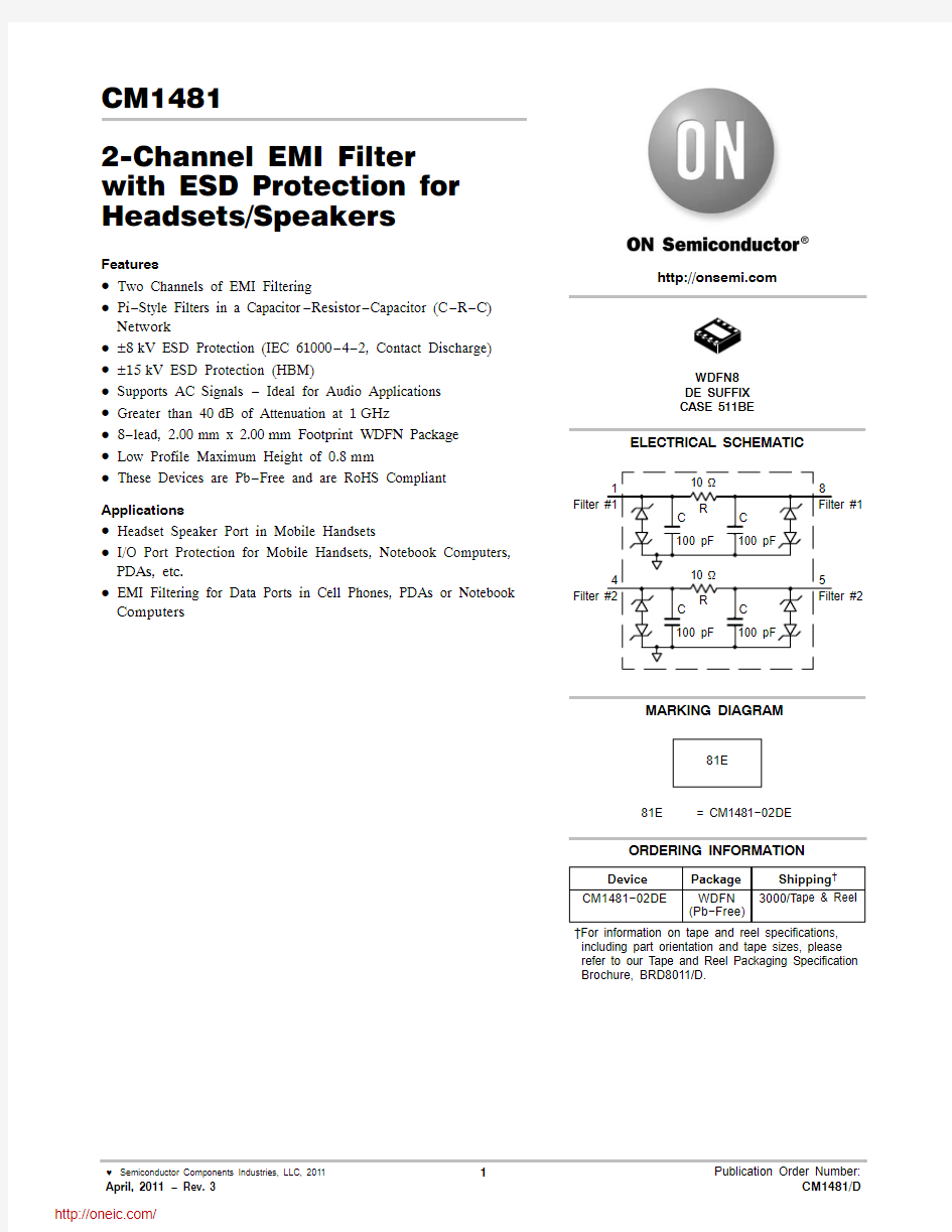
?Two Channels of EMI Filtering
?Pi ?Style Filters in a Capacitor ?Resistor ?Capacitor (C ?R ?C)Network
?±8kV ESD Protection (IEC 61000?4?2, Contact Discharge)?±15kV ESD Protection (HBM)
?Supports AC Signals ? Ideal for Audio Applications ?Greater than 40dB of Attenuation at 1GHz
?8?lead, 2.00mm x 2.00mm Footprint WDFN Package ?Low Profile Maximum Height of 0.8mm
?
These Devices are Pb ?Free and are RoHS Compliant
Applications
?Headset Speaker Port in Mobile Handsets
?I/O Port Protection for Mobile Handsets, Notebook Computers,PDAs, etc.
?
EMI Filtering for Data Ports in Cell Phones, PDAs or Notebook Computers
MARKING DIAGRAM
Device Package Shipping ?ORDERING INFORMATION
https://www.doczj.com/doc/861184302.html,
CM1481?02DE
WDFN (Pb ?Free)
3000/T ape & Reel
?For information on tape and reel specifications,including part orientation and tape sizes, please refer to our Tape and Reel Packaging Specification Brochure, BRD8011/D.
81E = CM1481?02DE
ELECTRICAL SCHEMATIC
WDFN8DE SUFFIX CASE 511BE
81E
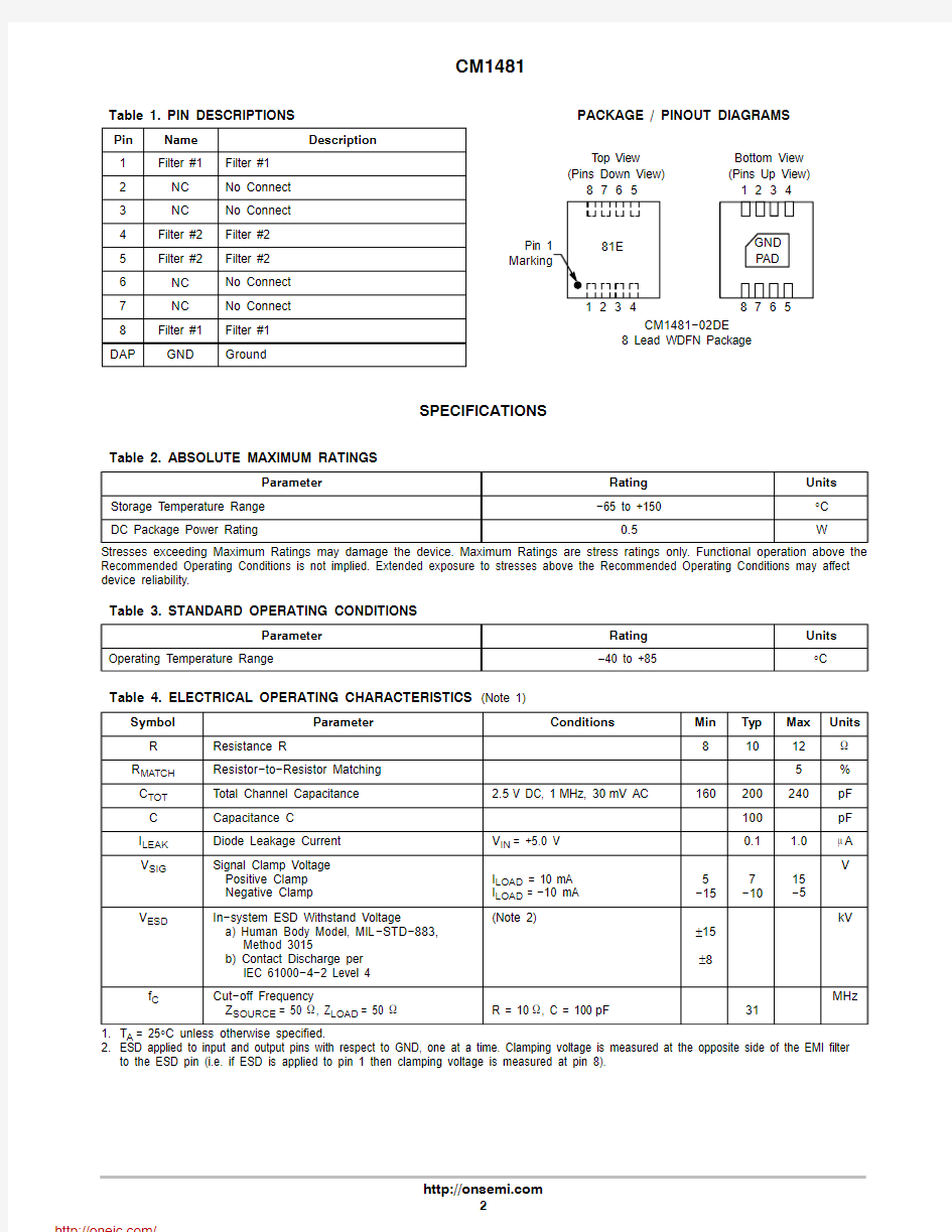
Table 1. PIN DESCRIPTIONS
Pin Name Description
1Filter #1Filter #12NC No Connect 3NC No Connect 4Filter #2Filter #25Filter #2Filter #26NC No Connect 7NC No Connect 8Filter #1Filter #1
DAP
GND
Ground
Top View (Pins Down View)
Bottom View (Pins Up View)CM1481?02DE 8 Lead WDFN Package
PACKAGE / PINOUT DIAGRAMS
SPECIFICATIONS
Table 2. ABSOLUTE MAXIMUM RATINGS
Parameter
Rating Units Storage Temperature Range ?65 to +150
°C DC Package Power Rating
0.5
W
Stresses exceeding Maximum Ratings may damage the device. Maximum Ratings are stress ratings only. Functional operation above the Recommended Operating Conditions is not implied. Extended exposure to stresses above the Recommended Operating Conditions may affect device reliability.
Table 3. STANDARD OPERATING CONDITIONS
Parameter
Rating Units Operating Temperature Range
–40 to +85
°C
Table 4. ELECTRICAL OPERATING CHARACTERISTICS (Note 1)
Symbol Parameter
Conditions
Min Typ Max Units R Resistance R
8
10
12W R MATCH Resistor ?to ?Resistor Matching 5%C TOT Total Channel Capacitance 2.5V DC, 1MHz, 30mV AC
160
200240
pF C Capacitance C 100pF I LEAK Diode Leakage Current V IN = +5.0 V 0.1 1.0m A V SIG
Signal Clamp Voltage Positive Clamp Negative Clamp
I LOAD = 10 mA I LOAD = ?10 mA 5?157?10
15?5
V
V ESD
In ?system ESD Withstand Voltage
a) Human Body Model, MIL ?STD ?883, Method 3015
b) Contact Discharge per IEC 61000?4?2 Level 4(Note 2)
±15±8
kV
f C
Cut ?off Frequency
Z SOURCE = 50 W , Z LOAD = 50 W
R = 10W , C = 100pF 31
MHz
1.T A = 25°C unless otherwise specified.
2.ESD applied to input and output pins with respect to GND, one at a time. Clamping voltage is measured at the opposite side of the EMI filter to the ESD pin (i.e. if ESD is applied to pin 1 then clamping voltage is measured at pin 8).
PERFORMANCE INFORMATION
Typical Filter Performance (nominal conditions unless specified otherwise, 50 W Environment)
Figure 1. Insertion Loss vs. Frequency (Filter #1 to GND B2)
Figure 2. Insertion Loss vs. Frequency (Filter #2 to GND B2)
PACKAGE DIMENSIONS
WDFN8 2x2, 0.5P
CASE 511BE?01
ISSUE O Array .
DIMENSIONS: MILLIMETERS
*For additional information on our Pb?Free strategy and soldering
details, please download the ON Semiconductor Soldering and
Mounting Techniques Reference Manual, SOLDERRM/D.
ON Semiconductor and are registered trademarks of Semiconductor Components Industries, LLC (SCILLC). SCILLC reserves the right to make changes without further notice to any products herein. SCILLC makes no warranty, representation or guarantee regarding the suitability of its products for any particular purpose, nor does SCILLC assume any liability arising out of the application or use of any product or circuit, and specifically disclaims any and all liability, including without limitation special, consequential or incidental damages.
“Typical” parameters which may be provided in SCILLC data sheets and/or specifications can and do vary in different applications and actual performance may vary over time. All operating parameters, including “Typicals” must be validated for each customer application by customer’s technical experts. SCILLC does not convey any license under its patent rights nor the rights of others. SCILLC products are not designed, intended, or authorized for use as components in systems intended for surgical implant into the body, or other applications intended to support or sustain life, or for any other application in which the failure of the SCILLC product could create a situation where personal injury or death may occur. Should Buyer purchase or use SCILLC products for any such unintended or unauthorized application, Buyer shall indemnify and hold SCILLC and its officers, employees, subsidiaries, affiliates, and distributors harmless against all claims, costs, damages, and expenses, and reasonable attorney fees arising out of, directly or indirectly, any claim of personal injury or death associated with such unintended or unauthorized use, even if such claim alleges that SCILLC was negligent regarding the design or manufacture of the part. SCILLC is an Equal Opportunity/Affirmative Action Employer. This literature is subject to all applicable copyright laws and is not for resale in any manner.
PUBLICATION ORDERING INFORMATION
分销商库存信息: ONSEMI
CM1481-02DE