
收稿日期:2007206210
基金项目:国家重大基础研究(973)资助(51327020301)作者简介:岳远征(19812),男,西安电子科技大学博士研究生,E 2mail :yzhyue @https://www.doczj.com/doc/7b18731990.html,.
A l Ga N /Ga N H EM Ts 表面钝化抑制电流崩塌的机理研究
岳远征,郝 跃,张进城,冯 倩
(西安电子科技大学微电子学院,陕西西安 710071)
摘要:通过实验测量对Al G aN/G aN H EM T 表面钝化抑制电流崩塌的机理进行了深入研究.Al G aN/
G aN H EM T Si 3N 4钝化层使用PECVD 获得.文章综合考虑了钝化前后器件输出特性及泄漏电流的变
化,钝化后直流电流崩塌明显减少,仍然存在小的崩塌是由于GaN 缓冲层中的陷阱对电子的捕获.传输
线模型测量表明,钝化后电流的增加是由于钝化消除了表面态密度进而增加了沟道载流子密度.
关键词:高电子迁移率晶体管;钝化;电流崩塌
中图分类号:TN386 文献标识码:A 文章编号:100122400(2008)0120125204
Mechanism study of the surface passivation effect on current collapse
characteristics of Al G a N/G a N HEMTs
YU E Yuan 2z heng ,H A O Yue ,Z H A N G J i n 2cheng ,F EN G Qi an
(School of Microelectronic ,Xidian Univ.,Xi ′an 710071,China )
Abstract : The effects of surface passivation on Al GaN/G aN high 2electron 2mobility transistors
(H EM Ts )have been investigated.The surface passivation layer of Si 3N 4is deposited by plasma
enhanced chemical vapor deposition (PECVD ).The current 2voltage and gate 2drain diode characteristics
of Al G aN/G aN H EM Ts before and after passivation are analyzed.The current collapse under DC sweep
has been significantly decreased after passivation and the existence of small dispersion of drain current is
due to traps in the G aN buffer.The drain current increases after passivation ,because surface passivation
reduces the surface state density and so increases the sheet carrier density shown in Transmission Linear
Model (TL M )measurement.
K ey Words : high electron mobility transistors ;passivation ;current collap se
The Al GaN/GaN material system for high power applications has advantages of a larger band 2gap (314eV ),a larger critical breakdown electric field (3MV/cm ),larger conduction band discontinuity between GaN and Al GaN and strong polarization effect s t hat allow a large two 2dimensional elect ron gas (2DEG )concent ratio n (>1013cm -2)which is larger t han t hat of Al GaAs/GaAs to be confined.Based on t hese properties ,dramatic progress has been made in t he develop ment of Al GaN/GaN high 2elect ron 2mobility t ransistors (H EM Ts )as an ideal candidate for high power and high temperat ure applications at microwave f requencies.One of t he f requently reported p roblems is t hat t he RF power obtained from GaN 2based H EM Ts is much lower t han t hat expected f rom t he DC characteristics [1~3].Several mechanisms have been identified ,including t he presence of surface states between t he gate and drain of t he H EM T struct ure which deplete t he channel in t his region wit h time constant s long enough to disrupt t he modulation of t he channel charge during large signal operation and t he t rap states in t he GaN buffer layer [3].The main obstacle to t he develop ment of GaN 2based high power devices has been ,and co ntinues to be ,how to cont rol t he t rap densities in t he bulk and surface of t he material.Surface t rapping effect s is present in
2008年2月
第35卷 第1期 西安电子科技大学学报(自然科学版)
J OU R NAL O F XI D IAN U N IV E R S I T Y Feb.2008
Vol.35 No.1
virt ually all devices ,and significantly impacte current collap se.Much attention has been focused on t he reduction of surface states using different passivation dielect rics [2~6].
In t his paper ,t he mechanisms of Si 3N 4surface passivatio n on Al GaN/GaN H EM Ts are st udied.In addition ,unpassivated H EM Ts are also compared wit h passivated
ones.
Fig.1 Typical Al G aN/GaN H EM T
cross section.1 Materials grow th and device fabrication
Our st ruct ure was grown by metal 2organic chemical vapor
depo sitio n and consist s of a 40nm undoped AlN buffer layer ,a
1μm undoped GaN layer ,and a 25nm n 2Al 013Ga 017N barrier layer
on a 22in.sapp hire substrate.The room temperat ure Hall mobility
of 1096cm 2/(V ?s )and a sheet carrier concent ration of 1165×
1013cm -2have been measured respectively.Figure 1shows a
representative cro ss section of Al GaN/GaN H EM Ts.
In t he devices discussed in t his paper ,t he source 2drain spacing is 5μm and gate lengt h is 2μm.Typical source 2gate and gate 2drain
spacings are 1μm and 2μm ,respectively.
The device p rocess follows standard H EM T processing technology.Mesa isolation is formed by Cl 22based ICP etch ,and follows Ti/Al/Ni/Au ohmic contact depo sition by elect ron 2beam evaporation and annealing at 850°C for 30s.The metal scheme of Pt/Au is utilized for gate metals.
After all t he device processes ,t he passivation layer was deposited.A low 2temperat ure (300°C ),plasma 2enhanced chemical vapor depo sition p rocess using Si H 4and N H 3was used to deposit Si 3N 4wit h a t hickness of 2×10⁻⁷m and a ref raction index of 1197which were measured by an ellip someter.The Si 3N 4layer above t he pads was etched wit h t he BO E solution.DC measurement s were performed on t he fabricated devices using a H P4156B
unit.
Fig.2 I ds vs.V ds double sweep f rom 021020V for H EM Ts before and after Si 3N 4,passivation.
2 Experimental results and discussion
Figure 2shows typical outp ut characteristics of t he double
sweep for Al GaN/GaN H EM Ts before and after Si 3N 4passivation.
V g is fixed at 0V ,and V ds sweep s f rom 0to 10V ,and t hen t he sweep
is repeated wit hout pause.The decrease in drain current between
first sweep and second sweep was pronounced before passivation.
The degradation in drain current was less significant when t he same
st ruct ures were grown on SiC subst rates [7].Clo ser lattice match
between GaN and SiC was discovered t han t hat wit h sapp hire.So t he
defect density will be lower between GaN and SiC.This seems to affect t he resultant surface state density.It is suggested t hat some of t he surface trap s be related to dismatch between GaN and sapp hire.Shown in Figure 2is an evident improvement of current after t he passivation.On t he ot her hand ,t he DC dispersion is still present in t he device after t he surface passivation.The reason is t he p resence of trap s in t he GaN buffer layer under t he active channel.Some electrons of t he 2DEG can be depleted due to t he surface states or buffer t rap s.The former may be mitigated to a greater or less extent by app rop riate surface passivation ,which most often uses Si 3N 4depo sited by plasma 2enhanced chemical vapor deposition ,while t he latter is a f unction of t he epitaxial
6
21 西安电子科技大学学报(自然科学版) 第35卷
growt h conditions.In t his paper ,surface states dominate t he current collap se ,because t he use of Si 3N 4passivation typically restores 70%~80%of t he lo st current.The increased drain current directly influences t he outp ut power.The device outp ut power (P out )is calculated wit h (V ds 2V knee )(I d /2),where V ds is t he applied drain source bias ,V knee is t he drain source bias where t he linear regime changes to sat uration regime ,and I d is t he drain current.A higher P out is observed in Si 3N 4passivated H EM Ts.
Figure 3shows t he I ds 2V ds characteristics before and after Si 3N 4passivation.The I ds increases after Si 3N 4passivatio n ,which indicates t hat t he surface state density is decreased.After passivation t he t hreshold voltage is shifted to negative values ,which is due to t he increase of 2DEG density.This increase of t he sheet carrier concent ration in 2DEG due to t he change of t he surface states after passivation is t he main reason for t he increased drain current.At p resent ,t he reason for t his increase is due to a reduction in surface depletion effect s or an additional charge cont ributio n f rom t he deposited nit ride layer.It is found in Figure 3t hat an increase in I d and g m has been observed on t he passivated Si 3N 4H EM Ts compared wit h t he unpassivated H EM Ts when V gs is below 0V.The observation of t he current reduction when V gs is above 0V f rom Si 3N 4passivated H EM Ts is due to t he formation of deep t rap s in t he Si 3N 4/Al GaN interface along wit h t he elimination of shallow t rap s t hrough t he PECVD depo sition [8].The kink or current collap se when V gs is above 0V is obvious on t he passivated H EM Ts.Similar behaviors were observed on Si 3N 4passivated Al GaN/GaN H EM Ts by Ando et al [9]
.
Fig.3 I ds vs.V ds for H EM Ts
before and after Si 3N 4passivation.Fig.4 G ate 2drain diode characteristics for H EM Ts before and after Si 3N 4passivation.
The effect of passivation o n t he gate 2to 2drain diode I 2V characteristics is shown in Figure 4.The gate current measured at a voltage of -40V decreased f rom 140μA to 25μA after passivation.An about one order of magnit ude lower I g was observed on Si 3N 4passivated H EM Ts.This improvement in I g 2leak is
due Fig.5 Relation of TL M resistance and length.
to t he depletion layer formed ,resulting in t he reduction of t he
electric field strengt h at t he gate edge toward t he drain.The
reduction of t he elect ric field at t he gate edge result s in lower
electrons injectio n in surface states t rap s.S.Arulkumaran [8]reported
t hat an about o ne order of magnit ude lower I g 2leak was observed on
Si 3N 4passivated H EM Ts ,as compared wit h t he unpassivated
H EM Ts.This is similar to our experimental result shown in Figure
4. B.L uo [7]reported t he different result t hat t he increase in gate
leakage is not f ro m t he passivation it self ,but may originate f rom
degradatio n of t he gate metallization during t he oxide desorption step
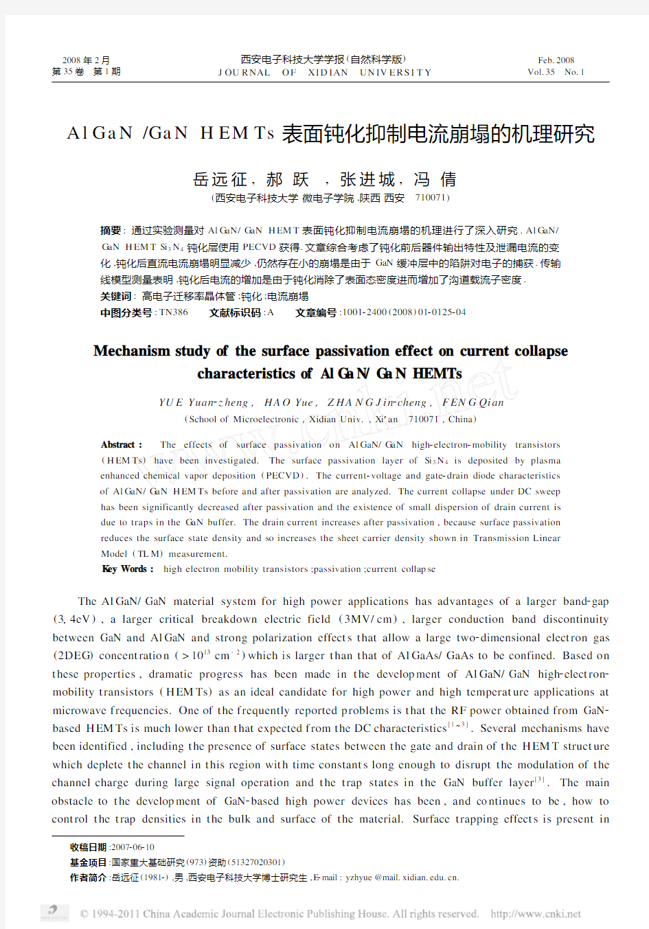
at 350°C.Figure 5shows t he curve of t he relation between TL M resistance and lengt h.We can see t hat t he TL M resistance declines obviously.This result can be explained by a reduction in surface depletion effect s 721第1期 岳远征等:Al GaN/G aN H EM Ts 表面钝化抑制电流崩塌的机理研究
821 西安电子科技大学学报(自然科学版) 第35卷or an additional charge contribution from t he deposited nit ride layer after passivation.
3 Conclusion
We have demonst rated t he surface passivation effect s on t he performance of Al GaN/GaN H EM Ts by depo siting Si3N4wit h PECVD.An increase in drain current has been observed on t he passivated Si3N4 H EM Ts compared wit h t he unpassivated H EM Ts.An about one order of magnit ude lower I g2leak is observed on Si3N4passivated H EM Ts.This indicates an important improvement of device p roperties despite of t he fact t hat t he DC dispersion is still present after t he passivatio n process which is due to t he p resence of t rapping centers in t he resistive buffer underlying t he active channel.
Reference:
[1]Vetury R,Zhang N Q,Keller S.The Impact of Surface States on the DC and RF Characteristics of Al G aN/GaN HFETs
[J].IEEE Trans on Electron Devices,2001,48(3):5602566.
[2]Arulkumaran S,Egawa T,Ishikawa H.Investigations of SiO2/n2G aN and Si3N4/n2G aN Insulator2semiconductor
Interfaces with Low Interface State Density[J].Appl Phys Lett,1998,73(6):8092812.
[3]Green B M,Chu K K,Chumbes E M.The Effect of Surface Passivation on the Microwave Characteristics of Undoped
Al GaN/G aN H EM Ts[J].IEEE Electron Device Lett,2000,21(3):2682271.
[4]L u W,Kumar V.A Comparative Study of Surface Passivation on Al G aN/GaN H EM Ts[J].Solid State Electronics,
2002,46(6):144121445.
[5]Vertiachikh A V,Eastman L F.Effect of Surface Passivation of Al G aN/GaN Heterostructure Field2effect Transistor[J].
Electron Lett,2002,38(5):3882391.
[6]Dang X Z,Yu E T,Piner E J.Influence of Surface Processing and Passivation on Carrier Concentrations and Transport
Properties in Al GaN/G aN Heterostructures[J].J Appl Phys,2001,90(9):135721362.
[7]L uo B,Mehandru R,Kim J,et https://www.doczj.com/doc/7b18731990.html,parison of Surface Passivation Films for Reduction of Current Collapse in Al G aN/
G aN High Electron Mobility Transistors[J].Journal of The Electrochemical Society,2002,149(11):6132619.
[8]Arulkumaran S,Egawa T,Ishikawa H.Surface Passivation Effects on Al G aN/G aN High2electron2mobility Transistors
with SiO2,Si3N4,and Silicon Oxynitride[J].Appl Phys Lett,2004,84(4):6132615.
[9]Ando Y,Okamoto Y,Miyamoto H.A1102W Heterojunction Fet on Thinned Sapphire Substrate[J].IEDM Tech Dig,
2001,17(3):3812384.
(编辑:齐淑娟) 简 讯
2007年11月8日~9日,法国Thales公司的Francois Le Chevalier先生来我校讲
学访问.Chevalier先生是IEEE的高级会员,曾在法国宇航局ON EAR领导研究雷
达目标识别、目标和背景信号、雷达建模和雷达信号处理.1998年起从事机载雷达、
电子战、机载任务系统的高级研发等工作.
摘自《西电情况》2007.12.10
A A 模拟 A/DC模拟信号到数字信号的转换A/L音频/逻辑板 AAFPCB音频电路板 AB 地址总线 ab 地址总线 accessorier 配件ACCESSORRIER 配件 ADC(A/O)模拟到数字的转换adc 模拟到数字的转换ADDRESS BUS地址总线 AFC 自动频率控制 afc 自动频率控制 AFC自动频率控制 AFMS 来音频信号 afms 来自音频信号 AFMS来音频信号 AFPCB 音频电路板 AF音频信号 AGC 自动增益控制 agc 自动增益控制AGC自动增益控制aged 模拟地 AGND 模拟地AGND模拟地ALARM 告警 alarm 告警 ALC 自动电平控制ALEV 自动电平 AM 调幅 AMP 放大器 AMP放大器 AM调幅 ANT 天线 ANT/SW 天线开关ant 天线 Anternna天线 antsw 天线开关ANTSW天线切换开关ANT天线 APC 自动功率控制APC/AOC自动功率控制ARFCH 绝对信道号
ASIC 专用接口集成电路AST-DET 饱和度检测ATMS 到移动台音频信号atms 到移动台音频信号ATMS到移动台音频信号AUC 身份鉴定中心AUDIO 音频 AUDIO音频 AUTO自动 AUX辅助 AVCC音频处理芯片 A模拟信号 b+ 内电路工作电压BALUN平衡于一不平衡转换BAND-SEL频段选择/切换BAND频段 Base band基带(信号) base 三极管基极 batt+ 电池电压 BDR接收数据信号 Blick Diagram方框图 BPF带通滤波器BUFFER缓冲放大器 BUS通信总线 buzz 蜂鸣器 C CALL 呼叫 CARD 卡 Carrier载波调制 CCONTCSX开机维持(NOKIA) CCONTINT关机请求信号 CDMA 码分多址 cdma 码分多址 CEPT 欧洲邮电管理委员会 CH 信道 CHAGCER 充电器 CHECK 检查 CIRCCITY 整机 Circuit Diagram电路原理图 CLK 时钟 CLK-OUT逻辑时钟输出 CLK-SELECT时钟选择信号(Motorola 手机) COBBA音频IC(诺基亚系列常用)
《电路分析基础B》课程教学大纲(56+0学时) 一、课程基本情况 二.课程性质与任务 《电路分析基础》是电类专业的一门重要的学科基础课。本课程的主要任务是研究电路的基本定理、定律、基本分析方法及应用。本课程的目标是使学生通过对本课程的学习,理解电路分析的基本概念,掌握其分析方法、定理和定律并能灵活应用于电路分析中,使学生在分析问题和解决问题的能力上得到培养和提高,为后续课程的学习奠定坚实的理论基础。 课程思政部分要求:在教学过程中融入爱国教育、社会责任、人生领悟、民族自信、感恩等多种育人要素,倡导科学研究中的科学精神、创新精神和工匠精神,实现教师和学生的知识、情感及价值等方面的共鸣。 三. 课程主要教学内容及学时分配
四.课程教学基本内容和基本要求 第一章基础知识( 5学时) [知识点]:电路分析基本变量(电流、电压和功率)的概念;线性电阻元件和独立源的定义及伏安关系;基尔霍夫电流定律和基尔霍夫电压定律;受控源。 [重点] 电流、电压、功率及参考方向的概念,电路的两类约束关系(元件约束和拓扑约束) [难点] 电流、电压真实方向与参考方向关系、关联非关联参考下功率计算及功率正负含义,受控源电路分析 [基本要求] 1、理解电路分析基本变量(电流、电压和功率)的概念;2、掌握线性电阻元件和独立源的定义及伏安关系;3、熟练掌握基尔霍夫电流定律和基尔霍夫电压定律;4、理解受控源的概念。 [实践与练习] 课后作业布置建议: 习题:1-1、1-2、1-3 、1-5、1-6、1-12、1-9、1-13、1-17 、1-30、1-31。 课程思政映射点:由电压、电流单位以物理学家伏特和安培名字命名,以及基尔霍夫21岁提出基尔霍夫定律,引导学生敬畏科学家、崇尚科学精神。 第二章等效变换分析法( 5学时) [知识点]:单口网络等效条件;实际电源的两种电路模型及其等效变换;无源和含源单口网络的等效化简;T~π等效变换。 [重点]:单口网络的等效条件,单口网络的等效化简方法;
UREGISTERED未注册 SW开关 UI用户接口BSIC专用集成电路 BAND频段 BAND-SEL频段选择/切换 BUFFER缓冲放大器 BUS通信总线 DET检测 Circuit Diagram电路原理图 Blick Diagram方框图 PCB板图 LayoutPCB元件分布图 Receiver收信机 Transmitter发信机 Interface界面,电子电路基础知识2,接口 Power Supply电源系统 射频电路 A模拟信号 AFC自动频率控制 AGC自动增益控制 APC/AOC自动功率控制 AGND模拟地 ANT天线 ANTSW天线切换开关 AM调幅 BPF带通滤波器 CP-TX RXVCO控制输出接收锁相电平 CP-TX TXVCO控制输出发射锁相电平 DUPLEX / DIPLEX双工器 Duplex Sapatation双工间隔 DCS-CS发射机控制信号:控制TXVCO与I/Q调制器FILFTER滤波器 Gen Out信号发生器 GAIN增益 GSM-PINDIODE功率放大器输出匹配电路切换控制信号GSM-SEL频段切换控制信号之一 G-TX-VCO900MHZ发射VCO切换控制 IF中频 IFLO中频本振 LO本振 LOCK锁定 MODFreq调制频率 Mixed Second第二混频信号
PLL锁相环路 PADRV功率放大器驱动 TXRF发射射频 TXEN发射使能 TXENT发射供电 TXIN发送I信号负 TXIP发送I信号正 TXON发送开 TXQN发送Q信号负 TXQP发送Q信号正 TXI发射基带信号 TX-DEY-OUT发射时序控制输出 TXQ发射基带信号 UHFVCO超高频/射频VCO VHFVCO甚高频/中频VCO SHFVCO专用射频VCO(NOKIA) VCO 压控振荡器 VCTCXO温补压控振荡器 AMP放大器 CTL-GSM频段控制信号 Diplex双工滤波器 SUPLEX双工器作用相当于天线开关 LPF低通滤波器 MAINVCO主振荡器(Motorola) MIX混频器 Anternna天线 RFConnector射频接口 BALUN平衡于一不平衡转换 Direct Coner Siorl Lionear Receicer直接变换的线性接收机Carrier载波调制 POWCONTROL功率控制 POWLEV功放级别 RFIN/OFF高频输入/输出 RADIO射频本振 RFADAT射频频率合成器数据 RFAENB射频频率合成器启动 RSSI接收信号强度指示 RX接收 RXIN接收输出 RXON接收机启动/开关控制 RXOUT接收输出 RXEN接收使能 RXIFN接收中频信号负
Econometrics report Class number: No number: Eglish name: Chinese name:
Contents Background and Data Analysis 2-5 and model T-test 6-8 F-test 8-10 Summary,and,suggestion 11
BACKGROUND ●The report below is about the food sales , I instance the resident population (10 000 ) , per capita income the first year , meat sales , egg sales , the fish sales . ●In order to build mathematical models to understand the relationship of each variable and its food sales , and I take statistics of Tianjin from 1994 to 2007 the demand for food Among Y X1 X2 X3 X4 X5 1 98.4500 153.2000 560.2000 6.5300 1.2300 1.8900 2 100.7000 190.0000 603.1100 9.1200 1.3000 2.0300 3 102.8000 240.3000 668.0500 8.1000 1.8000 2.7100 4 133.9500 301.1200 715.4700 10.1000 2.0900 3.0000 5 140.1300 361.0000 724.2700 10.9300 2.3900 3.2900 6 143.1100 420.0000 736.1300 11.8500 3.9000 5.2400 7 146.1500 491.7760 748.9100 12.2800 5.1300 6.8300 8 144.6000 501.0000 760.3200 13.5000 5.4700 8.3600 9 146.9400 529.2000 774.9200 15.2900 6.0900 10.0700 10 158.5500 552.7200 785.3000 18.1000 7.9700 12.5700 11 169.6800 771.7600 795.5000 19.6100 10.1800 15.1200 12 162.1400 811.8000 804.8000 17.2200 11.7900 18.2500 13 170.0900 988.4300 814.9400 18.6000 11.5400 20.5900 14 178.6900 1094.6500 828.7300 23.5300 11.6800 23.3700
《电子技术基础实验Ⅰ》课程教学大纲 课程英文名称:Fundadamentals of Electronic Technology Lab Ⅰ 课程代码:E0200710 学时数:20 学分数:1 课程类型:实验课程 适用学科专业:电子类专业 先修课程:电路分析 执笔者:崔红玲编写日期:2013-11-15 审核人: 一、课程简介 本课程是电子信息工程、通信工程等电子类专业的一门重要实验课程,以“电路分析基础”作为背景知识,在服务于理论课程的同时,注重引导学生建立工程上的感性认识,认识常用的电子元器件,学会使用常用的电子测量仪器,学会简单的电子测量方法,能够设计搭建简单的单元电路。 一、Introduction This course is an important experiment course in electronic and communication engineering. Based on the “Basic Theories of Circuit Analysis”, this course not only serves for the theory courses, but also aims at helping students have a perceptual cognition on electronic engineering projects. Students in this course will be able to know about basic electronic components, use electronic measurement devices, handle simple electronic measurement methods, and design and build the basic circuit unit. 二、课程目标 引导学生建立工程上的感性认识,增强培养学生实践动手能力。通过设计单元电路引导 学生学会应用理论知识,通过预设的问题和实验中遇到的小故障,引导学生学会独立思考, 培养学学生独立分析问题、解决问题的能力。 二、Goals The course will guide the students to have a perceptual cognition on electronic engineering -on ability. Student will be able to apply the electronic theory and thus improve the students’ hands practically by designing the circuit unit. Also, They will have the ability to think independently by solving the problems and faults in the experiments. These teaching activities will enhance
手机电路图中英文对照 手机电路图中英文对照 A A 模拟 AB 地址总线ACCESSORIES 配件ADC 模拟到数字的转换ADDRESS BUS 地址总线 AFC 自动频率控制 AFPCB 音频电路板 AGC 自动增益控制 AGND 模拟地 ALARM 告警 ALERT 振铃 ALRT 铃声电路 ALRT-VCC 振铃器电源 ANTSW 天线开关 AOC-DRIVE 自动功率控制驱动AUDIO 音频 AUX 辅助 AVCC 音频供电 APC 音频处理芯片GSM-LNA275 900MHz低噪声放大器电压() GSM-PINDIODE 功率放大器输出到匹配电路的切换控制信号 GSM-SEL 频段切换控制信号之一(900 MHz) G-TX-VCO 900MHz发射压控振荡器 H Hex 十六进制 Hamonic Filter 谐波滤波器 HAND SET 手持机 HARDWARE 硬件 HOOK 外接免提计算机 HEAD-INT 头戴耳机控制 I Insert Card 插入卡 Initial 初始化 IMSI 国际移动用户识别码 IWF 各种业务功能接口 I/O 输入/输出 ICTRL 供电电流大小控制 IFLO 中频本振 INFRARED RAY 红外线 INT 中断 K KEYBOARD 键盘 KEY 键、键控 KHz 千赫兹 KBC 按键列地址线 L
ANT 天线 AUC 鉴权中心 A/D 模拟/数字转换AUTO 自动 A/L 音频/逻辑板ACCESS 接入 APC 自动功率控制 B BIT 比特 BURST 突发脉冲串BCCH 广播信道 BW 带宽 BUSY 忙 BUS 总线BARRING 限制 BCD 二/十进制码BPF 带通滤波器Block Digram 方框图Backlight 背光LPF 低通滤波器 LCD 液晶显示器 LCD DATA 显示屏数据 LCD EN 显示屏使能 LCD WR 显示屏写入 LINE 连接线、线路 LO 本振 LOCK 锁定 LOGIC 逻辑 LOOP FLITER 环路滤波器 LSPCTRL 扬声器控制 M MIN 移动用户电话识别码 MSN 机械序列号 MIC 拾音器 MS 移动台 MODEM 调制解调器 MENU 菜单 MOD Freq 调制频率 MCLK 主时锺 MDM 调制解调器 MEMORY 存储器 MISO 主机输入从机输出(摩托罗拉)Mixed Second 第二混频 MOBILE 移动 MOD 调制 MODIN 调制I信号负 MODIP 调制I信号正 MODQN 调制Q信号负 MODQP 调制Q信号正 MOSI 主机输出从机输入 MPU 主处理单元(中央处理器)MUC 主控制单元
实验报告 实验名称外贸英语函电系别经济与管理系年级专业 学生姓名 学号 指导老师 2012年11月15日
实验项目FULL IN APPLICATION FOR L/C Array实验地点:老图书馆机房_实验日期:2012年11月12日 一、实验目的 掌握涉及付款方面的专业词汇的表达,了解信用证的内容及对信用证进行正确的审核;能够独立的书写付款和结帐方面的函电,通过真实单证处理,掌握审单要点后能正确处理信用证业务,填写各种进出口业务议付单据。 二、实验内容 (1)了解信用证的内容及对信用证进行正确的审核,根据教学软件中提供的不同的案例内容,掌握审单要点后能正确处理信用证业务,填写各种进出口业务议付单据。 (2)根据合同及国际贸易惯例,根据资料1和资料3设计申请和审核信用证的方案与步骤,填写上述资料2信用证申请书;修改资料4信用证与合同不相符的地方。 三、实验仪器设备 (1)CPU2.0G,内存512M以上配置的计算机,安装有windows XP 操作系统(2)进出口单证系统、进出口场景英语软件 四、实验步骤 1.实验指导老师(即任课教师)介绍外贸单证教学系统的基本组成和操作步骤,在每节课的实验项目项目开始前,先由实验指导老师介绍本次课程的基本组成和操作步骤,然后在老师的指导与控制下,了解信用证的内容及对信用证进行正确的审核,了解与信用证与合同的关系,掌握审单要点后能正确处理信用证业务,填写各种进出口业务议付单据。 2.首先对外贸结汇单证进行填写及审核、对国际贸易真实单证进行识读;独立进行实验方案设计,完成实验方案设计报告;用英语设计单证处理系统,按自己拟定的信用证的申请和修改步骤及方案对信用证进行申请和修改。 3.先提交实验课程的实验任务的电子版,以邮件形式发给指导老师。再按照 指导老师的要求打印成纸版,作为实验报告的一部分提交给实验指导老师。
通信工程专业本科学分制培养方案 (一)专业培养目标 本专业培养具备通信技术、通信系统和通信网等方面的知识,能在通信领域中从事研究、设计、制造、运营及在国民经济各部门和国防工业中从事开发、应用通信技术与设备的高素质应用型工程技术人才。 (二)专业培养基本要求 本专业学生主要学习通信系统和通信网方面的基础理论、组成原理和设计方法,受到通信工程实践的基本训练,具备从事现代通信系统和网络的设计、开发、调测和工程应用的基本能力。 毕业生应获得以下几方面的知识和能力: 1、掌握通信领域内的基本理论和基础知识; 2、掌握光波、无线、多媒体等通信技术; 3、掌握通信系统和通信网的分析和设计方法; 4、具有设计、开发、调测、应用通信系统和通信网的基本能力; 5、了解通信系统和通信网建设的基本方针、政策和法规; 6、了解通信技术的最新进展与发展动态; 7、掌握文献检索、资料查询的基本方法,具有一定的科学研究和实际工作能力。 (三)主干学科 信息与通信工程、计算机科学与技术。 (四)主要课程 高等数学、大学物理学、电路分析基础、模拟电子技术、数字电子技术、信号与系统、通信电子线路、数字信号处理、现代通信原理、信息论与编码理论、现代交换原理、计算机通信网、移动通信、光纤通信、微型计算机原理与应用、电磁场与电磁波、单片机原理及应用等。 (五)主要实践性教学环节
(六)主要专业实验 本专业还开设以下主要非单列实验课程,学分与理论课统一计算,此处不单列: (七)修业年限及学分要求 1、学制:四年,修业年限:三至六年。 2、学分要求:修业期间至少需修完170学分。其中包括实践性教学项目19学分,公共选修课(含必读书目8个)16学分。 3、学分及比例: 公共必修课,共47学分,(包括社会实践2学分、军训2学分),占总学分27.6%; 专业必修课,共73学分(包括专业见习1学分,生产实习6学分,毕业设计8学分),占总学分42.9%; 专业选修课,需修满34学分,占总学分20%; 公共选修课,需修满16学分(包括必读书目8学分),占总学分9.4%。 4、公共选修课课程及学分按《延安大学本科学分制公共选修课实施办法》执行。 5、必读书目考核及学分按《延安大学本科生必读书目成绩考核办法》执行。 (八)授予学位和学位课程 授予学位:工学学士 学位课程:
实验项目名称:System analysis实验学时: 4 同组学生姓名:实验地点: 实验日期:实验成绩: 批改教师:批改时间: 一、实验目的和要求 To complete the SRS document and system Architectural analysis. 二、实验仪器和设备 硬件:PC 软件:Office 2010 Astah 三、实验过程 Library Management System(LMS) --Software Requirement Analysis 1. Introduction 1.1 The preparation of purpose The preparation of this requirement is to develop ways of LMS software research using large database foundation and application method. At the same time, it is also the foundation of project planning, preliminary design and detailed design, is the maintenance personnel perform internal maintenance, update, acceptance and test basis. Provided the development basis for software developers, since the directivity function in the process of software development. The main readers for software designers, programmers, and teacher. 1.2Scope of project The project name is " Library Management System". The main functions of the
《电路分析基础》课程教学大纲 课程英文名称:Theory of circuit 课程编号:1510064002 课程计划学时:80(授课学时:64 实验学时:16) 学分:4.5 课程简介: 电路分析基础课程是自动化、电气工程及其自动化、测控技术、电子信息工程、电子信息科学与技术、电子科学与技术、通讯工程等专业的一门重要技术基础课,通过本课程的学习,使学生掌握电路的基本理论,分析电路的基本方法,以及进行实验的初步技能,并为后续课准备必要的电路知识。电路分析基础课程理论严密,逻辑性强,对学生的辨证思维能力的培养和树立理论联系实际的科学观点及提高学生分析问题解决问题的能力,都有重要的作用。 一、课程教学内容及教学基本要求 第一章电路模型和电路定律 本章重点是电流和电压参考方向的概念、功率的计算、电路元件特性、以及基尔霍夫定律,难点是参考方向的概念及应用、基尔霍夫定律的应用。全章课堂讲授6学时,实验1学时。 第一节电路及电路模型 要求了解电路的作用(考核概率1%),理解实际电路的电路图和电路模型(考核概率1%),掌握电路的组成及各组成部分的作用(考核概率80%)。 1.电路的组成及各组成部分的作用:电源、负载和中间环节。 2.电路的作用:实现电能的传输和变换,实现信号的传递和处理。 3.实际电路的电路图和电路模型。 第二节电流、电压参考方向 理解电流、电压参考方向的含义(考核概率50%)。 第三节电功率和能量 理解功率的定义(考核概率50%),掌握功率的计算方法(考核概率80%)。 1.功率的定义 2.功率计算方法 第四节电路元件 要求了解电路集总参数的概念(考核概率1%)。
一、Basic Definitions Electron: an indivisible particle of negative charge. The amount of charge is measured in coulombs (C). The magnitude of the charge associated with an electron is 1.602x10-l9 C. Current: charge in motion (electrons). Current is measured in units of amperes, or more simply amp. Voltage: an electric potential difference that causes electron flow. It is also called electromotive force (EMF). An analogy often used to describe current and voltage is water in a pipe. Current is analogous to the flow of water, while voltage is analogous to the pressure. Conductor: a material that allows a continuous current to pass through it under the action of a fixed voltage. An example of a good conductor is copper or aluminum which is used in homes and offices for all electrical connections. Insulator: the opposite of a conductor, it does not allow a continuous current to pass though it under the action of a fixed voltage. An example of an insulator is the plastic on electrical cords. Using our water analogy, a conductor can be envisioned as the region inside a pipe, while an insulator can be envisioned as the actual material of the pipe which contains the water flow. Switch: used to control the flow of electrons, or current as it is commonly called. Ideally, a switch turns on or off instantly, and has no voltage across it while it is conducting. In our water analogy, an ideal switch would cut the flow immediately, from completely on to completely off in an instant. Common Passive Circuit Elements All circuit elements can be separated into two groups: active and passive. The electrical definition is very similar to the common definition: active circuit elements are capable of delivering power, while passive elements are capable of receiving, and possibly storing, power. In our water analogy, a pump would be an active element. A narrow section of pipe that restricts the flow, a tank, and a water wheel would all be examples of passive elements. Resistors: circuit elements that literally "resist" current flow. Voltage is higher on the end of the resistor that sees the current first. Figure 1 shows two schematic representations of a resistor. In our water analogy, a resistor would be a narrow section of pipe that restricts the flow.
精心整理 A A模拟 A/DC模拟信号到数字信号的转换A/L音频/逻辑板 AAFPCB音频电路板 AB地址总线 ab地址总线 accessorier配件ACCESSORRIER配件 ADC(A/O)模拟到数字的转换adc模拟到数字的转换ADDRESS BUS地址总线 AFC自动频率控制 afc自动频率控制 AFC自动频率控制 AFMS来音频信号 afms来自音频信号 AFMS来音频信号 AFPCB音频电路板 AF音频信号 AGC自动增益控制 agc自动增益控制 AGC自动增益控制 aged模拟地 AGND模拟地 AGND模拟地 ALARM告警 alarm告警 ALC自动电平控制 ALEV自动电平 AM调幅 AMP放大器 AMP放大器 AM调幅 ANT天线 ANT/SW天线开关 ant天线 Anternna天线 antsw天线开关 ANTSW天线切换开关 ANT天线 APC自动功率控制 APC/AOC自动功率控制 ARFCH绝对信道号ASIC专用接口集成电路 AST-DET饱和度检测 ATMS到移动台音频信号 atms到移动台音频信号 ATMS到移动台音频信号 AUC身份鉴定中心 AUDIO音频 AUDIO音频 AUTO自动 AUX辅助 AVCC音频处理芯片 A模拟信号 b+内电路工作电压 BALUN平衡于一不平衡转换 BAND-SEL频段选择/切换 BAND频段 Baseband基带(信号) base三极管基极 batt+电池电压 BDR接收数据信号 BlickDiagram方框图 BPF带通滤波器 BUFFER缓冲放大器 BUS通信总线 buzz蜂鸣器 C CALL呼叫 CARD卡 Carrier载波调制 CCONTCSX开机维持(NOKIA) CCONTINT关机请求信号 CDMA码分多址 cdma码分多址 CEPT欧洲邮电管理委员会 CH信道 CHAGCER充电器 CHECK检查 CIRCCITY整机 CircuitDiagram电路原理图 CLK时钟 CLK-OUT逻辑时钟输出 CLK-SELECT时钟选择信号(Motorola手机) COBBA音频IC(诺基亚系列常用) COL列 COLLECTOR集电极 CONTROL控制
大学物理实验报告 Ferroelectric Control of Spin Polarization Controlling the spin degree of freedom by purely electrical means is currently an important challenge in spintronics (1, 2). Approaches based on spin-transfer torque (3) have proven very successful in controlling the direction of magnetization in a ferromagnetic layer, but they require the injection of high current densities. An ideal solution would rely on the application of an electric field across an insulator, as in existing nanoelectronics. Early experiments have demonstrated the volatile modulation of spin-based properties with a gate voltage applied through a dielectric. Notable examples include the gate control of the spin-orbit interaction in III-V quantum wells (4), the Curie temperature T C(5), or the magnetic anisotropy (6) in magnetic semiconductors with carrier-mediated exchange interactions; for example, (Ga,Mn)As or (In,Mn)As. Electric field–induced modifications of magnetic anisotropy at room temperature have also been reported recently in ultrathin Fe-based layers (7, 8). A nonvolatile extension of this approach involves replacing the gate dielectric by a ferroelectric and taking advantage of the hysteretic response of its order parameter (polarization) with an electric field. When combined with (Ga,Mn)As channels, for instance, a remanent control of T C over a few kelvin was achieved through
《 电 路 分 析基础》各章习题案 第1章习题参考答案 1-1(1)50W ;(2)300V 、25V ,200V 、75V ;(3)R 2=12.5Ω,R 3=100Ω,R 4=37.5Ω 1-2VA=8.5V ,Vm=6.5V , VB=0.5V ,VC=-12V ,VD=-19V ,Vp=-21.5V ,U AB=8V ,U BC=12.5, U DA =-27.5V 1-3电源(产生:A 、 B 元件 ;负载 (吸收: C 、D 元件; 电 路满足 衡 条件。 1-4(1)VA=100V ,VB=99V ,VC=97V ,VD=7V ,VE=5V ,VF=1V ,UAF=99V ,UCE=92V , U BE =94V ,U BF =98V ,U CA =-3V ;(2)V C =90V ,V B =92V ,V A =93V ,V E =-2V ,V F =-6V , VG=-7V ,U AF=99V ,UCE=92V ,U BE=94V ,U BF=98V ,U CA=-3V 1-5I ≈0.18A ,6度,2.7元 1-6I=4A ,I 1=11A ,I 2=19A 1-7(a)U=6V ,(b)U=24V ,(c)R=5Ω,(d)I=23.5A 1-8(1)i6=-1A ;(2)u4=10V ,u6=3V ;(3)P1=-2W 发出,P2=6W 吸收,P3=16W 吸收, P 4=-10W 发出,P 5=-7W 发出,P 6=-3W 发出 1-9I=1A ,U S =134V ,R ≈7.8Ω 1-10S 断开:U AB=-4.8V ,UAO=-12V ,UBO=-7.2V ;S 闭合:UAB=-12V ,U AO=-12V ,UBO=0V 1-11 支路3,节点2,网孔2,回路3 1-12节点电流方程:(A)I 1+I 3-I 6=0,(B)I 6-I 5-I 7=0,(C)I 5+I 4-I 3=0 回路电压方程:①I 6R 6+U S5+I 5R 5-U S3+I 3R 3=0,②-I 5R 5-U S5+I 7R 7-U S4=0,③-I 3R 3+ US3+US4+I1R2+I1R1=0 1-13U AB =11V ,I 2=0.5A ,I 3=4.5A ,R 3≈2.4Ω 1-14V A =60V ,V C =140V ,V D =90V ,U AC =-80V ,U AD =-30V ,U CD =50V 1-15I1=-2A ,I2=3A ,I3=-5A ,I4=7A ,I5=2A 第2章习题参考答案 2-12.4Ω,5A 2-2(1)4V ,2V ,1V ;(2)40mA ,20mA ,10mA 2-31.5Ω,2A ,1/3A 2-46Ω,36Ω 2-52A ,1A 2-61A 2-72A 2-81A 2-9I1=-1.4A ,I2=1.6A ,I3=0.2A 2-10I 1=0A ,I 2=-3A ,P 1=0W ,P 2=-18W
Preparation of n -bromobutane 一、Purpose 1、Study the principle and method of preparing n-butyl bromide from n-butyl alcohol by treatment with sodium bromide and concentrated sulfuric acid 2、Learn the technique of reflux with a gas trap apparatus and washing. 二、Principle n-Butyl bromide can be easily prepared by allowing n-butyl alcohto react with sodium bromide and concentrated sulfuric acid. Main reactions : NaBr + H 2SO4 → HBr + NaHSO4 24 H SO 322232222CH CH CH CH OH HBr CH CH CH CH Br H O +???→+ Secondary reactions : 24H SO 32223222CH CH CH CH OH CH CH CH=CH H O ???→+; ()24H SO 32223222222CH CH CH CH OH CH CH CH CH O H O ???→+ 24222H SO HBr Br SO H O +??→++ 三、Materials n-butyl alcohol :4mL Sodium bromide :5g Concentrated sulfuric acid :2.5mL/6mL Anhydrous calcium chloride:0.5g 10% aqueous sodium hydroxide:5mL 四、Primary reagent And Product physical constants
EIE209 Basic Electronics Basic circuit analysis Prof. C.K. Tse: Basic Circuit Analysis1
Fundamental quantities ?Voltage — potential difference bet. 2 points ?“across” quantity ?analogous to ‘pressure’ between two points ?Current — flow of charge through a material ?“through” quantity analogous to fluid flowing along a pipe ? Prof. C.K. Tse: Basic Circuit
Units of measurement n Voltage: volt (V) n Current: ampere (A) n NOT Volt, Ampere!! Prof. C.K. Tse: Basic Circuit
Direction and polarity n Current direction indicates the direction of flow of positive charge n Voltage polarity indicates the relative potential between 2 points: + assigned to a higher potential point; and – assigned to a lower potential point. n NOTE: Direction and polarity are arbitrarily assigned on circuit diagrams. Actual direction and polarity will be governed by the sign of the value. Prof. C.K. Tse: Basic Circuit
英语论文之用新世纪高中英语教材,提高学生英语听说 能力的实验报告 从2001年9月,我校决定在高一年级全面试用新世纪英语教材,并成功申请了2001年的上海市教育发展基金,我荣幸地担当了该课题(课题号:J010057)组的负责人,进行了为期三年的课题研究,实验,经历了一系列的挑战,完成了高中三年新世纪教材的试用,取得了一定的成果。进行任何实验一定是有明确的实验目的,我校为了探索一条如何在新世纪英语教材这一舞台背景下,全面提高高中学生的英语语言能力,尤其是在传统上历来为中国学生弱项的英语听、说方面有所突破,决定在平行的10个班级中建立两个英语实验班。在编班之后的第一次摸底考试后,发现两个英语实验班的平均成绩要比平行班高3-4分(成绩见附表1)。所以我们在实验班的教学中,采取了一系列与平行班不同的方法和手段,在课堂教学中,除了运用新世纪英语教材之外,还适当补充了课外内容,增加了难度,以提高学生的语言能力。本文将重点讲述在三年的实验阶段中,如何着手解决听说困难这一难题。根据W.M.Rivers和M.S.Tmperly的统计显示,成人在交际活动中听,说,读,写所占的比例为: 言语活动形式听说读
写所占时 间比例45% 30% 16% 9% (舒运祥,1998,P148)听是四大语言技能中十分重要的组成 部分,也是日常交际活动中所占比例最大的。但是对以英语为非母语的 学生而言,却是不易掌握的一项技能。根据第二语言习得理论,语言输 入是语言习得的最基本条件,没有语言输入,就不可能有语言习得,因 此听力作为一种输入型技能在学生的语言习得中占有举足轻重的地位。 而说话能力是语言能力中一个非常重要的组成部分,而且是语言能力中 最容易让人直观地感受到一个人语言水平的一种技能。我国开展中学英 语教学时间不短了,但是一个让人困惑和烦恼的现实就是,我们培养的 学生,具有较强的英语解题能力,而开口说话的能力显然不够理想,众 所周知,听乃说的前提,听为说提供了物质基础,前者为语言输入,后 者为导出,要改变我们长期以来一直面临的哑巴英语的局面,我们觉得 首先必须为学生提供大量的听力材料,这一前提保证的条件下,再组织 各种话题,为学生提供英语交际的舞台。我们的具体做法如下:一、积 极促进课堂内外的英语交流,培养学生说英语的习惯首先,身为英语教 师的我,身体力行,所有英语课只使用英语这一语言频道,坚持在课堂 上,用英语进行交流。包括课间休息,谈心,也充分利用班主任身份,