
D Wake-Up From Standby Mode in Less Than 6 μs
D 16-Bit RISC Architecture,
125-ns Instruction Cycle Time
D 16-Bit Sigma-Delta A/D Converter With Internal Reference and Five Differential Analog Inputs
D 12-Bit D/A Converter
D Two Configurable Operational Amplifiers D 16-Bit Timer_A With Three Capture/Compare Registers D Brownout Detector D
Bootstrap Loader
D
MSP430FG42x0 Family Members Include:MSP430FG4250: 16KB+256B Flash Memory
256B RAM
MSP430FG4260: 24KB+256B Flash Memory
256B RAM
MSP430FG4270: 32KB+256B Flash Memory
256B RAM
D For Complete Module Descriptions, See MSP430x4xx Family User’s Guide ,Literature Number SLAU056
D
For Additional Device Information, See MSP430FG42x0 Device Erratasheet,Literature Number SLAZ038
description
The T exas Instruments MSP430 family of ultralow-power microcontrollers consist of several devices featuring different sets of peripherals targeted for various applications. The architecture, combined with five low-power modes, is optimized to achieve extended battery life in portable measurement applications. The device features a powerful 16-bit RISC CPU, 16-bit registers, and constant generators that contribute to maximum code efficiency. The digitally controlled oscillator (DCO) allows wake-up from low-power modes to active mode in less than 6 μs.
The MSP430FG42x0 is a microcontroller configuration with a 16-bit timer, a high-performance 16-bit sigma-delta A/D converter, 12-bit D/A converter, two configurable operational amplifiers, 32 I/O pins, and a liquid crystal display driver.
Typical applications for this device include analog and digital sensor systems, digital motor control, remote controls, thermostats, digital timers, hand-held meters, etc.
AVAILABLE OPTIONS
PACKAGED DEVICES
T A
PLASTIC 48-PIN SSOP
(DL)PLASTIC 48-PIN QFN
(RGZ)MSP430FG4250IDL
MSP430FG4250IRGZ ?40°°C
MSP430FG4260IDL MSP430FG4260IRGZ 40C to 85MSP430FG4270IDL
MSP430FG4270IRGZ
This integrated circuit can be damaged by ESD. Texas Instruments recommends that all integrated circuits be handled with appropriate precautions. Failure to observe proper handling and installation procedures can cause damage. ESD damage can range from subtle performance degradation to complete device failure. Precision integrated circuits may be more susceptible to damage because very small parametric changes could cause the device not to meet its published specifications. These devices have limited built-in ESD protection.
Copyright ? 2007, Texas Instruments Incorporated
Please be aware that an important notice concerning availability, standard warranty, and use in critical applications of Texas Instruments semiconductor products and disclaimers thereto appears at the end of this data sheet.
PRODUCTION DATA nformat on s current as of publ cat on date.Products conform to specifications per the terms of Texas Instruments standard warranty. Production processing does not necessarily include testing of all parameters.
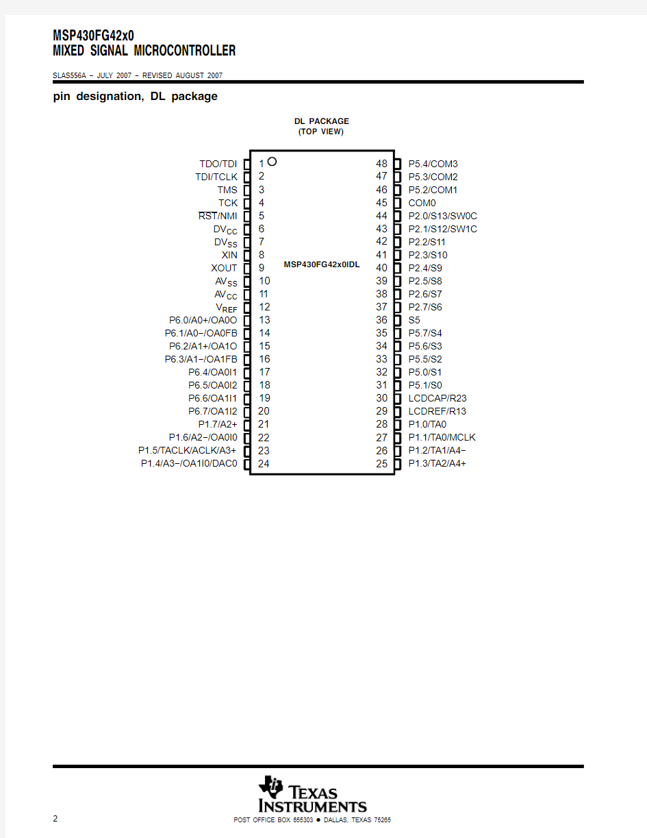
pin designation, DL package
P5.4/COM3P5.3/COM2P5.2/COM1COM0
P2.0/S13/SW0C P2.1/S12/SW1C P2.2/S11P2.3/S10P2.4/S9P2.5/S8P2.6/S7P2.7/S6S5
P5.7/S4P5.6/S3P5.5/S2P5.0/S1P5.1/S0
LCDCAP/R23LCDREF/R13P1.0/TA0
P1.1/TA0/MCLK P1.2/TA1/A4?P1.3/TA2/A4+
TDO/TDI TDI/TCLK
TMS TCK RST/NMI
DV CC DV SS XIN XOUT AV SS AV CC V REF
P6.0/A0+/OA0O P6.1/A0?/OA0FB P6.2/A1+/OA1O P6.3/A1?/OA1FB
P6.4/OA0I1P6.5/OA0I2P6.6/OA1I1P6.7/OA1I2P1.7/A2+
P1.6/A2?/OA0I0
P1.5/TACLK/ACLK/A3+P1.4/A3?/OA1I0/DAC0
DL PACKAGE (TOP VIEW)
pin designation, RGZ package
123425144756789101112151617181920212223
26272829303132
33343536464544434241403938
DV SS XIN XOUT AV CC AV SS V REF
P6.0/A0+/OA0O P6.1/A0?/OA0FB P6.2/A1+/OA1O P6.3/A1?/OA1FB
P6.4/OA0I1P6.5/OA0I2
P2.2/S11P2.3/S10P2.4/S9P2.5/S8P2.6/S7P2.7/S6S5P5.7/S4P5.6/S3P5.5/S2P5.0/S1P5.1/S0MSP430FG42x0IRGZ
P 6.6/O A 1I 1
P 6.7/O A 1I 2
P 1.7/A 2+
P 1.5/T A C L K /A C L K /A 3+P 1.6/A 2?/O A 0I 0
P 1.4/A 3?/O A 1I 0/D A C 0
P 1.3/T A 2/A 4+
P 1.2/T A 1/A 4?
P 1.1/T A 0/M C L K
P 1.0/T A 0
L C D R E F /R 13
L C D C A P /R 23
D V C C
R S T /N M I
T C K
T M S
T D I /T C L K
T D O /T D I
P 5.4/C O M 3
P 5.3/C O M 2
P 5.2/C O M 1C O M 0
P 2.0/S 13/S W 0C
P 2.1/S 12/S W 1C RGZ PACKAGE (TOP VIEW)
functional block diagram
DV
DV AV AV
Terminal Functions TERMINAL
NAME DL
NO.RGZ
NO.
I/O
DESCRIPTION
TDO/TDI143I/O Test data output. TDO/TDI data output or programming data input terminal
TDI/TCLK244I Test data input / test clock input. The device protection fuse is connected to TDI/TCLK. TMS345I Test mode select. TMS is used as an input port for device programming and test.
TCK446I Test clock. TCK is the clock input port for device programming and test.
RST/NMI547I General-purpose digital I/O / reset input / nonmaskable interrupt input
DV CC648Digital supply voltage, positive terminal
DV SS71Digital supply voltage, negative terminal
XIN82I Input terminal of crystal oscillator XT1
XOUT93O Output terminal of crystal oscillator XT1
AV SS104Analog supply voltage, negative terminal
AV CC115Analog supply voltage, positive terminal
V REF126I/O Analog reference voltage
P6.0/A0+/OA0O137I/O General-purpose digital I/O / analog input A0+ / OA0 output
P6.1/A0?/OA0FB148I/O General-purpose digital I/O / analog input A0? / OA0 feedback input
P6.2/A1+/OA1O159I/O General-purpose digital I/O / analog input A1+ / OA1 output
P6.3/A1?/OA1FB1610I/O General-purpose digital I/O / analog input A1? / OA1 feedback input
P6.4/OA0I11711I/O General-purpose digital I/O / OA0 input multiplexer on ?terminal
P6.5/OA0I21812I/O General-purpose digital I/O / OA0 input multiplexer on ?terminal
P6.6/OA1I11913I/O General-purpose digital I/O / OA1 input multiplexer on ?terminal
P6.7/OA1I22014I/O General-purpose digital I/O / OA1 input multiplexer on ?terminal
P1.7/A2+2115I/O General-purpose digital I/O / analog input A2+
P1.6/A2?/OA0I02216I/O General-purpose digital I/O / analog input A2? / OA0 input multiplexer on +terminal
P1.5/TACLK/ACLK/A3+2317I/O General-purpose digital I/O / Timer_A, clock signal TACLK input / ACLK output (divided by 1, 2, 4, or 8) / analog input A3+
P1.4/A3?/OA1I0/DAC02418I/O General-purpose digital I/O / analog input A3? / OA1 input multiplexer on +terminal / DAC12 output
P1.3/TA2/A4+2519I/O General-purpose digital I/O / Timer_A, Capture: CCI2A, compare: Out2 output / analog input A4+
P1.2/TA1/A4?2620I/O General-purpose digital I/O / Timer_A, Capture: CCI1A, compare: Out1 output / analog input A4?
P1.1/TA0/MCLK2721I/O General-purpose digital I/O / Timer_A. Capture: CCI0B / MCLK output. Note: TA0 is only an input on this pin / BSL Receive
P1.0/TA02822I/O General-purpose digital I/O / Timer_A. Capture: CCI0A input, compare: Out0 output / BSL transmit
LCDREF/R132923External LCD reference voltage input / input port of third most positive analog LCD level (V4
or V3)
LCDCAP/R233024Capacitor connection for LCD charge pump /
input port of second most positive analog LCD level (V2)
P5.1/S03125I/O General-purpose digital I/O / LCD segment output 0
P5.0/S13226I/O General-purpose digital I/O / LCD segment output 1
P5.5/S23327I/O General-purpose digital I/O / LCD segment output 2
P5.6/S33428I/O General-purpose digital I/O / LCD segment output 3
P5.7/S43529I/O General-purpose digital I/O / LCD segment output 4
S53630O LCD segment output 5
P2.7/S63731I/O General-purpose digital I/O / LCD segment output 6
P2.6/S73832I/O General-purpose digital I/O / LCD segment output 7
Terminal Functions (Continued) TERMINAL
NAME DL
NO.RGZ
NO.
I/O
DESCRIPTION
P2.5/S83933I/O General-purpose digital I/O / LCD segment output 8
P2.4/S94034I/O General-purpose digital I/O / LCD segment output 9
P2.3/S104135I/O General-purpose digital I/O / LCD segment output 10
P2.2/S114236I/O General-purpose digital I/O / LCD segment output 11
P2.1/S12/SW1C4337I/O General-purpose digital I/O / LCD segment output 12 / Low resistance switch to V SS
P2.0/S13/SW0C4438I/O General-purpose digital I/O / LCD segment output 13 / Low resistance switch to V SS COM04539O Common output. COM0?COM3 are used for LCD backplanes.
P5.2/COM14640I/O General-purpose digital I/O / common output. COM0?COM3 are used for LCD backplanes. P5.3/COM24741I/O General-purpose digital I/O / common output. COM0?COM3 are used for LCD backplanes. P5.4/COM34842I/O General-purpose digital I/O / common output. COM0?COM3 are used for LCD backplanes. QFN Pad NA None NA QFN package pad connection to DV SS is recommended.
General-Purpose Register Program Counter Stack Pointer Status Register Constant Generator General-Purpose Register General-Purpose Register General-Purpose Register PC/R0SP/R1SR/CG1/R2CG2/R3R4R5R12R13General-Purpose Register General-Purpose Register R6R7General-Purpose Register General-Purpose Register R8R9General-Purpose Register General-Purpose Register R10R11General-Purpose Register General-Purpose Register
R14R15
short-form description
CPU
The MSP430 CPU has a 16-bit RISC architecture that is highly transparent to the application. All operations, other than program-flow instructions,are performed as register operations in conjunction with seven addressing modes for source operand and four addressing modes for destination operand.
The CPU is integrated with 16 registers that provide reduced instruction execution time. The register-to-register operation execution time is one cycle of the CPU clock.
Four of the registers, R0 to R3, are dedicated as program counter, stack pointer, status register,and constant generator respectively. The remaining registers are general-purpose registers.
Peripherals are connected to the CPU using data,address, and control buses, and can be handled with all instructions.instruction set
The instruction set consists of 51 instructions with three formats and seven address modes. Each instruction can operate on word and byte data.Table 1 shows examples of the three types of instruction formats. Table 2 lists the address modes.
Table 1. Instruction Word Formats
Dual operands, source-destination e.g., ADD R4,R5R4 + R5 ???> R5Single operands, destination only e.g., CALL R8PC ??>(TOS), R8??> PC Relative jump, un/conditional
e.g., JNE
Jump-on-equal bit = 0
Table 2. Address Mode Descriptions
ADDRESS MODE
S D SYNTAX EXAMPLE OPERATION Register F F MOV Rs,Rd MOV R10,R11R10 —> R11Indexed
F F MOV X(Rn),Y(Rm)MOV 2(R5),6(R6)
M(2+R5)—> M(6+R6)Symbolic (PC relative)
F F MOV EDE,TONI M(EDE) —> M(TONI)Absolute F F MOV & MEM, & TCDAT M(MEM) —> M(TCDAT)Indirect F MOV @Rn,Y(Rm)MOV @R10,Tab(R6)M(R10) —> M(Tab+R6)
Indirect autoincrement F MOV @Rn+,Rm MOV @R10+,R11M(R10) —> R11R10 + 2—> R10Immediate
F
MOV #X,TONI
MOV #45,TONI #45 —> M(TONI)
NOTE:S = source D = destination
operating modes
The MSP430 has one active mode and five software selectable low-power modes of operation. An interrupt event can wake up the device from any of the five low-power modes, service the request, and restore back to the low-power mode on return from the interrupt program.
The following six operating modes can be configured by software:
D Active mode (AM)
?All clocks are active
D Low-power mode 0 (LPM0)
?CPU is disabled
ACLK and SMCLK remain active, MCLK is available to modules
FLL+ loop control remains active
D Low-power mode 1 (LPM1)
?CPU is disabled
ACLK and SMCLK remain active, MCLK is available to modules
FLL+ loop control is disabled
D Low-power mode 2 (LPM2)
?CPU is disabled
MCLK, FLL+ loop control, and DCOCLK are disabled
DCO’s dc-generator remains enabled
ACLK remains active
D Low-power mode 3 (LPM3)
?CPU is disabled
MCLK, FLL+ loop control, and DCOCLK are disabled
DCO’s dc-generator is disabled
ACLK remains active
D Low-power mode 4 (LPM4)
?CPU is disabled
ACLK is disabled
MCLK, FLL+ loop control, and DCOCLK are disabled
DCO’s dc-generator is disabled
Crystal oscillator is stopped
interrupt vector addresses
The interrupt vectors and the power-up starting address are located in the address range 0FFFFh to 0FFE0h.
The vector contains the 16-bit address of the appropriate interrupt-handler instruction sequence.
Table 3. Interrupt Sources, Flags, and Vectors of MSP430FG42x0 Configuration
INTERRUPT SOURCE INTERRUPT FLAG SYSTEM INTERRUPT
WORD
ADDRESS
PRIORITY
Power-Up External Reset
Watchdog
Flash Memory
PC Out-of-Range (see Note 4)
WDTIFG
KEYV
(see Note 1)
Reset0FFFEh15, highest
NMI
Oscillator Fault
Flash Memory Access Violation
NMIIFG (see Notes 1 and 3)
OFIFG (see Notes 1 and 3)
ACCVIFG (see Notes 1 and 3)
(Non)maskable
(Non)maskable
(Non)maskable
0FFFCh14
0FFFAh13
SD16_A SD16CCTLx SD16OVIFG,
SD16CCTLx SD16IFG
(see Notes 1 and 2)
Maskable0FFF8h12
0FFF6h11
Watchdog Timer WDTIFG Maskable0FFF4h10
0FFF2h9
0FFF0h8
0FFEEh7 Timer_A3TACCR0 CCIFG0 (see Note 2)Maskable0FFECh6
Timer_A3TACCR1 CCIFG1 and TACCR2 CCIFG2,
TAIFG (see Notes 1 and 2)
Maskable0FFEAh5
I/O Port P1 (Eight Flags)P1IFG.0 to P1IFG.7 (see Notes 1 and 2)Maskable0FFE8h4 DAC12DAC12_0IFG
(see Note 2)
Maskable0FFE6h3
0FFE4h2 I/O Port P2 (Eight Flags)P2IFG.0 to P2IFG.7 (see Notes 1 and 2)Maskable0FFE2h1 Basic Timer1BTIFG Maskable0FFE0h0, lowest NOTES: 1.Multiple source flags
2.Interrupt flags are located in the module.
3.(Non)maskable: the individual interrupt-enable bit can disable an interrupt event, but the general-interrupt enable cannot disable it.
4. A reset is generated if the CPU tries to fetch instructions from within the module register memory address range (0h?01FFh) or from
within unused address ranges (MSP430FG4270, MSP430FG4260: from 0300h to 0BFFh and from 01100h to 07FFFh,
MSP430FG4250: from 0300h to 0BFFh and from 01100h to 0BFFFh).
special function registers (SFRs)
The MSP430 SFRs are located in the lowest address space and are organized as byte-mode registers. SFRs should be accessed with byte instructions.
interrupt enable registers 1 and 2
Address 0h
WDTIE:Watchdog-timer interrupt enable. Inactive if watchdog mode is selected.Active if watchdog timer is configured as a general-purpose timer.OFIE:Oscillator-fault-interrupt enable NMIIE:Nonmaskable-interrupt enable ACCVIE:
Flash access violation interrupt enable
Address 01h
rw–0
BTIE:Basic timer interrupt enable
interrupt flag registers 1 and 2
Address 02h
WDTIFG:Set on watchdog timer overflow (in watchdog mode) or security key violation Reset on V CC power-on or a reset condition at the RST/NMI pin in reset mode OFIFG:Flag set on oscillator fault NMIIFG:
Set via RST/NMI pin
Address 03h
rw–0
BTIFG:Basic timer flag
module enable registers 1 and 2
Address
04h
Address
05h
rw–0,1:Legend: rw:
Bit Can Be Read and Written
Bit Can Be Read and Written. It Is Reset or Set by PUC.Bit Can Be Read and Written. It Is Reset or Set by POR.SFR Bit Not Present in Device
rw–(0,1):
memory organization
MSP430FG4250
MSP430FG4260MSP430FG4270Memory
Main: interrupt vector Main: code memory Size Flash Flash 16KB
0FFFFh ? 0FFE0h 0FFFFh ? 0C000h 24KB
0FFFFh ? 0FFE0h 0FFFFh ? 0A000h 32KB
0FFFFh ? 0FFE0h 0FFFFh ? 08000h Information memory Size Flash 256 Byte 010FFh ? 01000h 256 Byte 010FFh ? 01000h 256 Byte 010FFh ? 01000h Boot memory Size ROM 1KB
0FFFh ? 0C00h 1KB
0FFFh ? 0C00h 1KB
0FFFh ? 0C00h RAM Size 256 Byte 02FFh ? 0200h 256 Byte 02FFh ? 0200h 256 Byte 02FFh ? 0200h Peripherals
16-bit 8-bit 8-bit SFR
01FFh ? 0100h 0FFh ? 010h 0Fh ? 00h
01FFh ? 0100h 0FFh ? 010h 0Fh ? 00h
01FFh ? 0100h 0FFh ? 010h 0Fh ? 00h
bootstrap loader (BSL)
The MSP430 BSL enables users to program the flash memory or RAM using a UART serial interface. Access to the MSP430 memory via the BSL is protected by user-defined password. For complete description of the features of the BSL and its implementation, see the application report Features of the MSP430 Bootstrap Loader , literature number SLAA089.
BSL Function DL Package Pins
RGZ Package Pins
Data Transmit 28 - P1.022 - P1.0Data Receive
27 - P1.1
21 - P1.1
flash memory
The flash memory can be programmed via the JTAG port, the bootstrap loader, or in-system by the CPU. The CPU can perform single-byte and single-word writes to the flash memory. Features of the flash memory include:
D Flash memory has n segments of main memory and two segments of information memory (A and B) of
128 bytes each. Each segment in main memory is 512 bytes in size.
D Segments 0 to n may be erased in one step, or each segment may be individually erased.D Segments A and B can be erased individually, or as a group with segments 0 to n.
Segments A and B are also called information memory.
D New devices may have some bytes programmed in the information memory (needed for test during
manufacturing). The user should perform an erase of the information memory prior to the first use.
Main Memory
Information Memory
32KB 0FFFFh 0FE00h 0FDFFh 0FC00h 0FBFFh 0FA00h 0F9FFh
08400h 083FFh
08200h 081FFh
08000h 010FFh
01080h 0107Fh
01000h
24KB 0FFFFh 0FE00h 0FDFFh 0FC00h 0FBFFh 0FA00h 0F9FFh
0A400h 0A3FFh 0A200h 0A1FFh 0A000h 010FFh 01080h 0107Fh 01000h
16KB 0FFFFh 0FE00h 0FDFFh 0FC00h 0FBFFh 0FA00h 0F9FFh
0C400h 0C3FFh 0C200h 0C1FFh 0C000h 010FFh 01080h 0107Fh 01000h
peripherals
Peripherals are connected to the CPU through data, address, and control buses and can be handled using all instructions. For complete module descriptions, refer to the MSP430x4xx Family User’s Guide, literature number SLAU056.
oscillator and system clock
The clock system in the MSP430FG42x0 family of devices is supported by the FLL+ module, which includes support for a 32768-Hz watch crystal oscillator, an internal digitally-controlled oscillator (DCO) and a high-frequency crystal oscillator. The FLL+ clock module is designed to meet the requirements of both low system cost and low-power consumption. The FLL+ features digital frequency locked loop (FLL) hardware that, in conjunction with a digital modulator, stabilizes the DCO frequency to a programmable multiple of the watch crystal frequency. The internal DCO provides a fast turn-on clock source and stabilizes in less than 6 μs. The FLL+ module provides the following clock signals:
D Auxiliary clock (ACLK), sourced from a 32768-Hz watch crystal or a high-frequency crystal
D Main clock (MCLK), the system clock used by the CPU
D Sub-Main clock (SMCLK), the sub-system clock used by the peripheral modules
D ACLK/n, the buffered output of ACLK, ACLK/2, ACLK/4, or ACLK/8
brownout
The brownout circuit is implemented to provide the proper internal reset signal to the device during power-on and power-off. The CPU begins code execution after the brownout circuit releases the device reset. However, V CC may not have ramped to V CC(min) at that time. The user must ensure the default FLL+ settings are not changed until V CC reaches V CC(min).
digital I/O
There are four 8-bit I/O ports implemented—ports P1, P2, P5, and P6:
D All individual I/O bits are independently programmable.
D Any combination of input, output, and interrupt conditions is possible.
D Edge-selectable interrupt input capability for all the eight bits of ports P1 and P2.
D Read/write access to port-control registers is supported by all instructions.
Basic Timer1
Basic Timer1 has two independent 8-bit timers that can be cascaded to form a 16-bit timer/counter. Both timers can be read and written by software. Basic Timer1 can be used to generate periodic interrupts.
LCD driver with regulated charge pump
The LCD_A driver generates the segment and common signals required to drive an LCD display. The LCD_A controller has dedicated data memory to hold segment drive information. Common and segment signals are generated as defined by the mode. Static, 2?MUX, 3?MUX, and 4?MUX LCDs are supported by this peripheral.
The module can provide a LCD voltage independent of the supply voltage via an integrated charge pump.
Furthermore, it is possible to control the level of the LCD voltage and thus contrast in software.
watchdog timer
The primary function of the watchdog timer (WDT+) module is to perform a controlled system restart after a software problem occurs. If the selected time interval expires, a system reset is generated. If the watchdog function is not needed in an application, the module can be configured as an interval timer and can generate interrupts at selected time intervals.
Timer_A3
Timer_A3 is a 16-bit timer/counter with three capture/compare registers. Timer_A3 can support multiple capture/compares, PWM outputs, and interval timing. Timer_A3 also has extensive interrupt capabilities.Interrupts may be generated from the counter on overflow conditions and from each of the capture/compare registers.
Timer_A3 Signal Connections
Input Pin Number Output Pin Number Device Input Signal Module Input Name Module
Module Output
DL RGZ Input Name Block
Signal
DL
RGZ
23 - P1.5
17 - P1.5
TACLK TACLK ACLK ACLK SMCLK
SMCLK Timer
NA
23 - P1.517 - P1.5TACLK INCLK 28 - P1.022 - P1.0TA0CCI0A 28 - P1.0
22 - P1.0
27 - P1.1
21 - P1.1
TA0CCI0B DV SS GND CCR0
TA0
DV CC
V CC 26 - P1.220 - P1.2TA1CCI1A 26 - P1.2
20 - P1.2
26 - P1.2
20 - P1.2
TA1CCI1B DV SS GND CCR1
TA1
DV CC
V CC 25 - P1.3
19 - P1.3
TA2CCI2A 25 - P1.3
19 - P1.3
ACLK (internal)
CCI2B DV SS GND CCR2
TA2
DV CC
V CC
SD16_A
The SD16_A module supports 16-bit analog-to-digital conversions. The module implements a 16-bit sigma-delta core and reference generator. In addition to external analog inputs, an internal V CC sense and temperature sensor are also available.
DAC12
The DAC12 module is a 12-bit, R-ladder, voltage output DAC. The DAC12 may be used in 8- or 12-bit mode.
operational amplifier (OA)
The MSP430FG42x0 has two configurable low-current general-purpose operational amplifiers. Each OA input and output terminal is software-selectable and offers a flexible choice of connections for various applications.The OAs primarily support front-end analog signal conditioning prior to analog-to-digital conversion.
OA Signal Connections
Input Pin Number Output Pin Number Device Input Signal
Module Input Name Module
Module Output
DL RGZ Input Name Block
Signal
DL RGZ 22 - P1.616 - P1.6OA0I0OA0I013 - P6.0
7 - P6.0
17 - P6.411 - P6.4OA0I1OA0I118 - P6.512 - P6.5OA0I2OA0I2OA0
OA0O
14 - P6.18 - P6.1OA0FB OA0FB 24 - P1.418 - P1.4OA1I0OA1I015 - P6.0
9 - P6.0
19 - P6.613 - P6.6OA1I1OA1I120 - P6.714 - P6.7OA1I2OA1I2OA1
OA1O
16 - P6.1
10 - P6.1
OA1FB
OA1FB
peripheral file map
PERIPHERALS WITH WORD ACCESS
Watchdog Watchdog timer control WDTCTL0120h
Timer_A3Capture/compare register 2TACCR20176h _
Capture/compare register 1TACCR10174h
Capture/compare register 0TACCR00172h
Timer_A register TAR0170h
Capture/compare control 2TACCTL20166h
Capture/compare control 1TACCTL10164h
Capture/compare control 0TACCTL00162h
Timer_A control TACTL0160h
Timer_A interrupt vector TAIV012Eh Flash Flash control 3FCTL3012Ch
Flash control 2FCTL2012Ah
Flash control 1FCTL10128h DAC12DAC12_0 data DAC12_0DAT01C8h
DAC12_0 control DAC12_0CTL01C0h
SD16_A
(see also Peripherals With Byte Access)General control
Channel 0 control
Interrupt vector word register
Channel 0 conversion memory
SD16CTL
SD16CCTL0
SD16IV
SD16MEM0
0100h
0102h
0110h
0112h PERIPHERALS WITH BYTE ACCESS
OA/GND Switches Switch control register SWCTL0CFh
OA1Operational amplifier 1 control register 1
Operational amplifier 1 control register 0OA1CTL1
OA1CTL0
0C3h
0C2h
OA0Operational amplifier 0 control register 1
Operational amplifier 0 control register 0OA0CTL1
OA0CTL0
0C1h
0C0h
SD16_A
(see also: Peripherals with Word Access)Channel 0 input control
Analog enable
SD16INCTL0
SD16AE
0B0h
0B7h
LCD_A LCD voltage control 1
LCD voltage control 0
LCD voltage port control 1
LCD voltage port control 0
LCD memory 20
:
LCD memory 16
LCD memory 15
:
LCD memory 1
LCD control and mode LCDAVCTL1 LCDAVCTL0 LCDAPCTL1 LCDAPCTL0
LCDM20
:
LCDM16
LCDM15
:
LCDM1
LCDACTL
0AFh
0AEh
0ADh
0ACh
0A4h
:
0A0h
09Fh
:
091h
090h
peripheral file map (continued)
PERIPHERALS WITH BYTE ACCESS (CONTINUED)
FLL+ Clock FLL+ Control 1FLL_CTL1054h
FLL+ Control 0FLL_CTL0053h
System clock frequency control SCFQCTL052h
System clock frequency integrator SCFI1051h
System clock frequency integrator SCFI0050h
Basic Timer1BT counter 2
BT counter 1
BT control BTCNT2
BTCNT1
BTCTL
047h
046h
040h
Port P6Port P6 selection P6SEL037h
Port P6 direction P6DIR036h
Port P6 output P6OUT035h
Port P6 input P6IN034h
Port P5Port P5 selection P5SEL033h
Port P5 direction P5DIR032h
Port P5 output P5OUT031h
Port P5 input P5IN030h
Port P2Port P2 selection P2SEL02Eh
Port P2 interrupt enable P2IE02Dh
Port P2 interrupt-edge select P2IES02Ch
Port P2 interrupt flag P2IFG02Bh
Port P2 direction P2DIR02Ah
Port P2 output P2OUT029h
Port P2 input P2IN028h
Port P1Port P1 selection P1SEL026h
Port P1 interrupt enable P1IE025h
Port P1 interrupt-edge select P1IES024h
Port P1 interrupt flag P1IFG023h
Port P1 direction P1DIR022h
Port P1 output P1OUT021h
Port P1 input P1IN020h
Special functions SFR module enable 2ME2005h p
SFR module enable 1ME1004h
SFR interrupt flag 2IFG2003h
SFR interrupt flag 1IFG1002h
SFR interrupt enable 2IE2001h
SFR interrupt enable 1IE1000h
absolute maximum ratings over operating free-air temperature (unless otherwise noted)?
Voltage applied at V CC to V SS ?0.3 V to 4.1 V . . . . . . . . . . . . . . . . . . . . . . . . . . . . . . . . . . . . . . . . . . . . . . . . . . . . . . Voltage applied to any pin (see Note 1) ?0.3 V to V CC + 0.3 V . . . . . . . . . . . . . . . . . . . . . . . . . . . . . . . . . . . . . . . . Diode current at any device terminal . ±2 mA . . . . . . . . . . . . . . . . . . . . . . . . . . . . . . . . . . . . . . . . . . . . . . . . . . . . . . Storage temperature, T stg :Unprogrammed device ?55°C to 150°C
. . . . . . . . . . . . . . . . . . . . . . . . . . . . . . . . . . . Programmed device ?40°C to 85°C
. . . . . . . . . . . . . . . . . . . . . . . . . . . . . . . . . . . . . . ?
Stresses beyond those listed under “absolute maximum ratings” may cause permanent damage to the device. These are stress ratings only, and functional operation of the device at these or any other conditions beyond those indicated under “recommended operating conditions” is not implied. Exposure to absolute-maximum-rated conditions for extended periods may affect device reliability.
NOTE 1:All voltages referenced to V SS. The JTAG fuse-blow voltage, V FB , is allowed to exceed the absolute maximum rating. The voltage is
applied to the TDI/TCLK pin when blowing the JTAG fuse.
recommended operating conditions
MIN
NOM
MAX UNIT Supply voltage during program execution (see Note 1), V CC (AV CC = DV CC = V CC )
1.8 3.6V Supply voltage during flash memory programming (see Note 1),V CC (AV CC = DV CC = V CC )
2.5
3.6V Supply voltage, V SS
(AV SS = DV SS = V SS )00V Operating free-air temperature, T A
?40
85
°C
LF selected,XTS_FLL=0
Watch crystal 32.768
LFXT1 crystal frequency, f (LFXT1)XT1 selected,XTS_FLL=1Ceramic resonator 4508000kHz
(see Note 2)
XT1 selected,XTS_FLL=1
Crystal 10008000Processor frequency (signal MCLK)f V CC = 1.8 V DC 4.15Processor frequency (signal MCLK), f
(System)V CC = 3.6 V
DC 8
MHz NOTES: 1.It is recommended to power AV CC and DV CC from the same source. A maximum difference of 0.3 V between AV CC and DV CC can
be tolerated during power up and operation.
2.In LF mode, the LFXT1 oscillator requires a watch crystal. In XT1 mode, LFXT1 accepts a ceramic resonator or a crystal.
1.8
3.6
34.15 MHz
8 MHz
Supply Voltage ? V
2.5
f System (MHz)
Figure 1. Frequency vs Supply Voltage, Typical Characteristic
electrical characteristics over recommended operating free-air temperature (unless otherwise noted)
supply current into AV CC + DV CC excluding external current
PARAMETER
TEST CONDITIONS
MIN
NOM MAX UNIT
Active mode (see Note 1), T 40°C to 85°C V CC = 2.2 V
250
370
I (AM)
f (MCLK) = f (SMCLK) = 1 MHz,f (ACLK) = 32,768 Hz XTS=0, SELM=(0,1)A = ?40C to 85
V CC = 3 V
400520μA Low-power mode (LPM0) T 40°C to 85°C
V CC = 2.2 V 5570I (LPM0)
Low power mode (LPM0) (see Note 1 and Note 4)A = ?40C to 85V CC = 3 V 95110μA
Low-power mode (LPM2), T 40°C to 85°C V CC = 2.2 V
11
14
I (LPM2)
f (MCLK) = f (SMCLK) = 0 MHz,f (ACLK) = 32,768 Hz, SCG0 = 0 (see Note 2 and Note 4)
A = ?40C to 85
V CC = 3 V
1722μA T A = ?40°C
1.0
2.0Low-power mode (LPM3),
T A = 25°C 22V
1.1
2.0Low-power mode (LPM3), = f = 0 MHz,T A = 60°C V CC = 2.2 V 2.0
3.0f (MCLK) f (SMCLK) 0 MHz,f (ACLK) = 32,768 Hz, SCG0 = 1
Basic Timer1enabled ACLK selected T A = 85°C 3.5 6.0I (LPM3)
Basic Timer1 enabled, ACLK selected LCD A enabled, LCDCPEN = 0 T A = ?40°C 1.8 2.8μA
LCD_A enabled, LCDCPEN = 0 (static mode, f = f (ACLK)/32), T A = 25°C 3V 1.6 2.7(,LCD ),(see Note 2, Note 3, and Note 4)
T A = 60°C V CC = 3 V 2.5 3.5T A = 85°C
4.27.5Low-power mode (LPM3),T A = ?40°C 2.5 3.5Low-power mode (LPM3), = f = 0 MHz,T A = 25°C = 2.2 V 2.5 3.5f (MCLK) f (SMCLK) 0 MHz,f (ACLK) = 32,768 Hz, SCG0 = 1Basic Timer1enabled ACLK selected T A = 85°C V CC 2.2 V 3.8 6.0I (LPM3)
Basic Timer1 enabled, ACLK selected LCD A enabled, LCDCPEN = 0 T A = ?40°C 2.9 4.0μA LCD_A enabled, LCDCPEN = 0 (4-mux mode, f = f (ACLK)/32), T A = 25°C = 3 V 2.9 4.0(,LCD ),(see Note 2, Note 3, and Note 4)
T A = 85°C V CC 3 V 4.47.5T A = ?40°C 0.10.5T A = 25°C
22V 0.10.5Low-power mode (LPM4)
T A = 60°C V CC = 2.2 V 0.7 1.1Low-power mode (LPM4), T A = 85°C 1.7 3.0I (LPM4)
f (MCLK) = 0 MHz, f (SMCLK) = 0 MHz,f = 0 Hz, SCG0 = 1 (N t 2d N t 4)
T A = ?40°C 0.10.8μA (ACLK)(see Note 2 and Note 4)T A = 25°C 3V 0.10.8T A = 60°C V CC = 3 V 0.8 1.2T A = 85°C
1.9
3.5
NOTES: 1.Timer_A is clocked by f (DCOCLK) = f (DCO) = 1 MHz. All inputs are tied to 0 V or to V CC . Outputs do not source or sink any current.
2.All inputs are tied to 0 V or to V CC . Outputs do not source or sink any current.
3.The LPM3 currents are characterized with a Micro Crystal CC4V?T1A (9 pF) crystal and OSCCAPx = 01h.
4.
Current for brownout included.
current consumption of active mode versus system frequency
I (AM) = I (AM) [1 MHz] × f (System) [MHz]
current consumption of active mode versus supply voltage
I (AM) = I (AM) [3 V] + 175 μA/V × (V CC – 3 V)
electrical characteristics over recommended operating free-air temperature (unless otherwise noted) (continued)
Schmitt-trigger inputs ? Ports P1, P2, P5, and P6; RST/NMI; JTAG: TCK, TMS, TDI/TCLK, TDO/TDI
PARAMETER TEST CONDITIONS MIN TYP MAX UNIT
Positive going input threshold voltage V CC = 2.2 V 1.1 1.55
V IT+Positive-going input threshold voltage
V CC = 3 V 1.5 1.98
V
Negative going input threshold voltage V CC = 2.2 V0.40.9
V IT?Negative-going input threshold voltage
V CC = 3 V0.9 1.3
V
Input voltage hysteresis(V V V CC = 2.2 V0.3 1.1
V hys Input voltage hysteresis (V IT+ ? V IT?)
V CC = 3 V0.51
V inputs Px.x, TAx
PARAMETER TEST CONDITIONS V CC MIN TYP MAX UNIT
External interrupt timing Port P1, P2: P1.x to P2.x, external trigger signal 2.2 V62
t(int)External interrupt timing for the interrupt flag, (see Note 1)
3 V50
ns
Timer A capture timing TA0TA1TA22.2 V62
t(cap)Timer_A capture timing TA0, TA1, TA2
3 V50
ns
Timer_A clock frequency
TACLK INCLK:t=t 2.2 V8
f(TAext)
externally applied to pin TACLK, INCLK:(H) = t(L)
3 V10
MHz
Timer A clock frequency SMCLK or ACLK signal selected 2.2 V8
f(TAint)Timer_A clock frequency SMCLK or ACLK signal selected
3 V10
MHz
NOTES: 1.The external signal sets the interrupt flag every time the minimum t(int)parameters are met. It may be set even with trigger signals shorter than t(int).
leakage current ? ports P1, P2, P5, and P6 (see Note 1)
PARAMETER TEST CONDITIONS MIN TYP MAX UNIT
I lkg(Px.y)Leakage
current Port Px V(Px.y) (see Note 2)V CC = 2.2 V/3 V±50nA
NOTES: 1.The leakage current is measured with V SS or V CC applied to the corresponding pin(s), unless otherwise noted.
2.The port pin must be selected as input.