ASM3P2863A
Peak EMI
Reducing Solution ?2010 SCILLC. All rights reserved.Publication Order Number: Features
? Generates an EMI optimized clock signal at the
output.
? Integrated loop filter components.
? Operates with a 3.3V / 2.5V supply.
? Operating current less than 4mA.
? CMOS design.
? Input frequency: 12MHz
? Generates a 1X low EMI spread spectrum clock of
the input frequency.
? Frequency deviation: ±0.4%(Typ) @ 12MHz Input
Frequency
? Available in 6L-TSOP (6L-TSOT-23) package.
Product Description
The ASM3P2863A is a versatile spread spectrum
frequency modulator designed specifically for a wide
range of clock frequencies. The ASM3P2863A reduces
electromagnetic interference (EMI) at the clock source,
allowing system wide reduction of EMI of all clock
dependent signals. The ASM3P2863A allows significant
system cost savings by reducing the number of circuit
board layers, ferrite beads and shielding that are
traditionally required to pass EMI regulations.
The ASM3P2863A uses the most efficient and optimized
modulation profile approved by the FCC and is
implemented by using a proprietary all digital method.
The ASM3P2863A modulates the output of a single PLL
in order to “spread” the bandwidth of a synthesized clock,
and more importantly, decreases the peak amplitudes of
its harmonics. This result in significantly lower system
EMI compared to the typical narrow band signal produced
by oscillators and most frequency generators. Lowering
EMI by increasing a signal’s bandwidth is called ‘spread
spectrum clock generation.’
Applications
The ASM3P2863A is targeted towards all portable
devices with very low power requirements like MP3
players, Notebooks and Digital still cameras.
Key Specifications
Description Specification
Supply voltages V DD = 2.5V / 3.3V
Cycle-to-Cycle Jitter ±200pS ( typ)
Output Duty Cycle 45/55% (worst case)
Modulation Rate Equation F IN/256
Frequency Deviation
±0.4 % (Typ) @ 12MHz
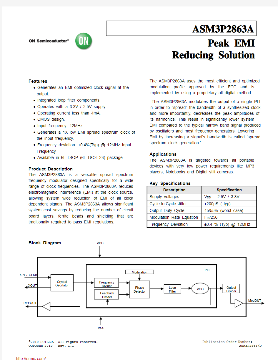
VDD
REFOUT ModOUT VSS
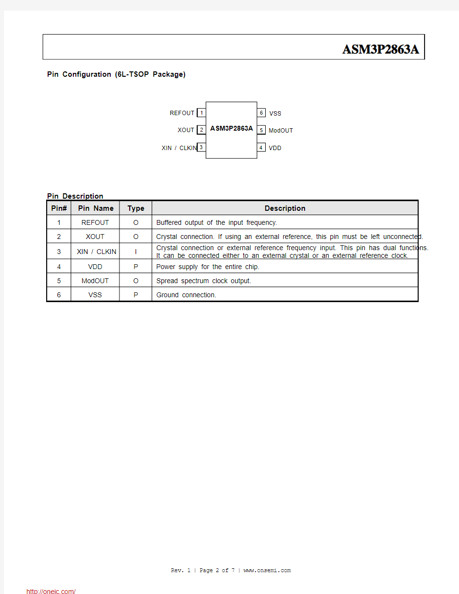
Pin Configuration (6L-TSOP Package)
Pin Description Pin#
Pin Name
Type
Description
1 REFOUT O Buffered output of the input frequency.
2 XOUT O Crystal connection. If using an external reference, this pin must be left unconnected.
3 XIN / CLKIN
I Crystal connection or external reference frequency input. This pin has dual functions. It can be connected either to an external crystal or an external reference clock. 4 VDD P Power supply for the entire chip. 5 ModOUT O Spread spectrum clock output. 6
VSS
P
Ground connection.
Absolute Maximum Ratings
Symbol Parameter Rating Unit VDD, V IN Voltage on any input pin with respect to Ground -0.5 to +4.6 V T STG Storage temperature -65 to +125 °C T s Max. Soldering Temperature (10 sec) 260 °C T J Junction Temperature 150 °C
2 KV
T DV Static Discharge Voltage
(As per JEDEC STD22- A114-B)
Note: These are stress ratings only and are not implied for functional use. Exposure to absolute maximum ratings for prolonged periods of time may affect device reliability.
Operating Conditions
Parameter Description Min Max Unit VDD Supply Voltage 2.375 3.6 V T A Operating Temperature (Ambient Temperature) 0 +70 °C
C L Load Capacitance 15 pF
C IN Input Capacitance 7 pF
DC Electrical Characteristics for 2.5V Supply
Symbol Parameter Min Typ Max Unit V IL Input low voltage VSS-0.3 0.8 V V IH Input high voltage 2.0 VDD+0.3 V
I IL Input low current -35 μA
I IH Input high current 35 μA
I XOL XOUT output low current (@ 0.5V, VDD = 2.5V) 3 mA
I XOH XOUT output high current (@ 1.8V, VDD = 2.5V) 3 mA
V OL Output low voltage (VDD = 2.5V, I OL = 8mA) 0.6 V V OH Output high voltage (VDD = 2.5V, I OH = 8mA) 1.8 V
I DD Static supply current1 0.8 mA
I CC Dynamic supply current (2.5V, 12MHz and no load) 3 mA
VDD Operating voltage 2.375 2.5 2.625 V t ON Power-up time (first locked cycle after power-up) 5 mS Z OUT Output impedance 50 ?Note: 1. XIN / CLKIN pin is pulled low.
AC Electrical Characteristics for 2.5V Supply
Symbol Parameter Min Typ Max Unit CLKIN Input frequency 12 MHz ModOUT Output frequency 12 MHz f d Frequency Deviation ±0.4 % t LH1Output rise time (measured from 0.7V to 1.7V) 0.5 1.5 1.7 nS t HL1Output fall time (measured from 1.7V to 0.7V) 0.5 1.0 1.2 nS t JC Jitter (Cycle-to-Cycle) ±200 ±300 pS t D Output duty cycle 45 50 55 % Note: 1. t LH and t HL are measured into a capacitive load of 15pF.
DC Electrical Characteristics for 3.3V Supply
Symbol Parameter Min Typ Max Unit V IL Input low voltage VSS-0.3 0.8 V V IH Input high voltage 2.0 VDD+0.3 V
I IL Input low current -35 μA
I IH Input high current 35 μA
I XOL XOUT output low current (@ 0.4V, V DD = 3.3V) 3 mA
I XOH XOUT output high current (@ 2.5V, V DD = 3.3V) 3 mA
V OL Output low voltage (VDD = 3.3V, I OL = 8mA) 0.4 V V OH Output high voltage (VDD = 3.3V, I OH = 8mA) 2.5 V
I DD Static supply current1 1 mA
I CC Dynamic supply current (3.3V, 12MHz and no load) 3.5 mA
VDD Operating Voltage 3.0 3.3 3.6 V t ON Power-up time (first locked cycle after power-up) 5 mS Z OUT Output impedance 45 ?Note: 1. XIN / CLKIN pin is pulled low.
AC Electrical Characteristics for 3.3V Supply
Symbol Parameter Min Typ Max Unit CLKIN Input frequency 12 MHz ModOUT Output frequency 12 MHz
f d Frequency Deviation ±0.4 %
t LH1Output rise time (measured from 0.8 to 2.0V) 0.5 1.4 1.6 nS
t HL1Output fall time (measured at 2.0V to 0.8V) 0.4 1.0 1.2 nS
t JC Jitter (Cycle-to-Cycle) ±200 ±300 pS
t D Output duty cycle 45 50 55 % Note: 1. t LH and t HL are measured into a capacitive load of 15pF.
Crystal Specifications
Fundamental AT cut parallel resonant crystal
Nominal frequency 12MHz
Frequency tolerance ±50ppm or better at 25°C Operating temperature range -25°C to +85°C Storage temperature -40°C to +85°C Load capacitance (C P ) 18pF
Shunt capacitance 7pF maximum ESR
25?
Note: C L is Load Capacitance and Rx is used to prevent oscillations at overtone frequency of the Fundamental frequency.
Typical Crystal Interface Circuit
Typical Application Schematic
ModOUT Clock
C L = 2*(C P – C S ), Where C
P = Load capacitance of crystal from crystal vendor datasheet.
C S = Stray capacitance due to C IN, PCB, Trace, etc.
Package Information
6L-TSOP Package
Symbol
Dimensions
Inches Millimeters Min Max Min Max
A …… 0.04 ….. 1.00 A1 0.00 0.004 0.00 0.10 A2 0.033 0.036 0.84 0.90 b 0.012 0.02 0.30 0.50 H 0.005 BSC 0.127 BSC
D 0.114 BSC 2.90 BSC
B 0.06 BS
C 1.60 BSC
e 0.0374 BSC 0.950 BSC
C 0.11 BSC 2.80 BSC
L 0.0118 0.02 0.30 0.50 θ0°4°0°4°
ON Semiconductor and are registered trademarks of Semiconductor Components Industries, LLC (SCILLC). SCILLC reserves the right to make changes without further notice to any products herein. SCILLC makes no warranty, representation or guarantee regarding the suitability of its products for any particular purpose, nor does SCILLC assume any liability arising out of the application or use of any product or circuit, and specifically disclaims any and all liability, including without limitation special, consequential or incidental damages. “Typical” parameters which may be provided in SCILLC data sheets and/or specifications can and do vary in different applications and actual performance may vary over time. All operating parameters, including “Typicals” must be validated for each customer application by customer's technical experts. SCILLC does not convey any license under its patent rights nor the rights of others. SCILLC products are not designed, intended, or authorized for use as components in systems intended for surgical implant into the body, or other applications intended to support or sustain life, or for any other application in which the failure of the SCILLC product could create a situation where personal injury or death may occur. Should Buyer purchase or use SCILLC products for any such unintended or unauthorized application, Buyer shall indemnify and hold SCILLC and its officers, employees, subsidiaries, affiliates, and distributors harmless against all claims, costs, damages, and expenses, and reasonable attorney fees arising out of, directly or indirectly, any claim of personal injury or death associated with such unintended or unauthorized use, even if such claim alleges that SCILLC was negligent regarding the design or manufacture of the part. SCILLC is an Equal Opportunity/Affirmative Action Employer. U.S Patent Pending; Timing-Safe and Active Bead are trademarks of PulseCore Semiconductor, a wholly owned subsidiary of ON Semiconductor. This literature is subject to all applicable copyright laws and is not for resale in any manner.
PUBLICATION ORDERING INFORMATION
LITERATURE FULFILLMENT:
Literature Distribution Center for ON Semiconductor P.O. Box 5163, Denver, Colorado 80217 USA Phone: 303-675-2175 or 800-344-3860 Toll Free USA/Canada
Fax: 303-675-2176 or 800-344-3867 Toll Free USA/Canada
Email: orderlit@https://www.doczj.com/doc/7312242693.html, N. American Technical Support: 800-282-9855
Toll Free USA/Canada
Europe, Middle East and Africa Technical
Support:
Phone: 421 33 790 2910
Japan Customer Focus Center
Phone: 81-3-5773-3850
ON Semiconductor Website:
https://www.doczj.com/doc/7312242693.html,
Order Literature: https://www.doczj.com/doc/7312242693.html,/orderlit
For additional information, please contact your
local Sales Representative
Ordering Information
Part Number Marking Package Type Temperature ASM3P2863AF-06OR V4L 6L-TSOP (6L-TSOT-23), TAPE & REEL,
Pb Free 0°C to +70°C A “microdot” placed at the end of last row of marking or just below the last row toward the center of package indicates Pb-free.
分销商库存信息: ONSEMI
ASM3P2863AF-06OR