Abstract Minimum-Buffered Routing of Non-Critical Nets for Slew Rate and Reliability Contro
- 格式:pdf
- 大小:164.61 KB
- 文档页数:8
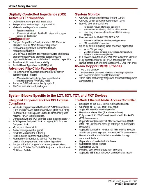
Virtex-5 Family OverviewDS100 (v5.1) August 21, 2015Product SpecificationDigitally Controlled Impedance (DCI)Active I/O Termination•Optional series or parallel termination •Temperature and voltage compensation •Makes board layout much easier−Reduces resistors −Places termination in the ideal location, at the signalsource or destination Configuration •Support for platform Flash, standard SPI Flash, or standard parallel NOR Flash configuration •Bitstream support with dedicated fallback reconfiguration logic •256-bit AES bitstream decryption provides intellectual property security and prevents design copying •Improved bitstream error detection/correction capability •Auto bus width detection capability •Partial Reconfiguration via ICAP port Advanced Flip-Chip Packaging •Pre-engineered packaging technology for proven superior signal integrity−Minimized inductive loops from signal to return −Optimal signal-to-PWR/GND ratios •Reduces SSO induced noise by up to 7x •Pb-Free and standard packages System Monitor •On-Chip temperature measurement (±4°C)•On-Chip power supply measurement (±1%)•Easy to use, self-contained −No design required for basic operation −Autonomous monitoring of all on-chip sensors −User programmable alarm thresholds for on-chip sensors•User accessible 10-bit 200kSPS ADC −Automatic calibration of offset and gain error −DNL = ±0.9 LSBs maximum •Up to 17 external analog input channels supported −0V to 1V input range −Monitor external sensors e.g., voltage, temperature −General purpose analog inputs •Full access from fabric or JT AG TAP to System Monitor •Fully operational prior to FPGA configuration and during device power down (access via JTAG T AP only)65-nm Copper CMOS Process • 1.0V Core Voltage •12-layer metal provides maximum routing capability and accommodates hard-IP immersion •Triple-oxide technology for proven reduced static power consumption System Blocks Specific to the LXT, SXT, TXT, and FXT DevicesIntegrated Endpoint Block for PCI ExpressCompliance•Works in conjunction with RocketIO GTP transceivers (LXT and SXT) and GTX transceivers (TXT and FXT)to deliver full PCI Express Endpoint functionality withminimal FPGA logic utilization.•Compliant with the PCI Express Base Specification 1.1•PCI Express Endpoint block or Legacy PCI Express Endpoint block•x8, x4, or x1 lane width •Power management support •Block RAMs used for buffering •Fully buffered transmit and receive •Management interface to access PCI Express configuration space and internal configuration•Supports the full range of maximum payload sizes •Up to 6x 32 bit or 3x 64 bit BARs (or a combination of 32 bit and 64 bit)Tri-Mode Ethernet Media Access Controller •Designed to the IEEE 802.3-2002 specification •Operates at 10, 100, and 1,000 Mb/s •Supports tri-mode auto-negotiation •Receive address filter (5 address entries)•Fully monolithic 1000Base-X solution with RocketIO GTP transceivers •Supports multiple external PHY connections (RGMII,GMII, etc.) interfaces through soft logic and SelectIO resources •Supports connection to external PHY device through SGMII using soft logic and RocketIO GTP transceivers •Receive and transmit statistics available through separate interface •Separate host and client interfaces •Support for jumbo frames •Support for VLAN •Flexible, user-configurable host interface •Supports IEEE 802.3ah-2004 unidirectional modeVirtex-5 Family OverviewDS100 (v5.1) August 21, 2015Product Specification Table 1:Virtex-5 FPGA Family Members Device Configurable Logic Blocks (CLBs)DSP48E Slices (2)Block RAM Blocks CMTs (4)PowerPC Processor Blocks Endpoint Blocks for PCI ExpressEthernet MACs (5)Max RocketIO Transceivers (6)Total I/O Banks (8)Max User I/O (7)Array (Row x Col)Virtex-5 Slices (1)Max Distributed RAM (Kb)18Kb (3)36Kb Max (Kb)GTP GTX XC5VLX3080x 304,8003203264321,1522N/A N/A N/A N/A N/A 13400XC5VLX50120x 307,2004804896481,7286N/A N/A N/A N/A N/A 17560XC5VLX85120x 5412,96084048192963,4566N/A N/A N/A N/A N/A 17560XC5VLX110160x 5417,2801,120642561284,6086N/A N/A N/A N/A N/A 23800XC5VLX155160x 7624,3201,6401283841926,9126N/A N/A N/A N/A N/A 23800XC5VLX220160x 10834,5602,2801283841926,9126N/A N/A N/A N/A N/A 23800XC5VLX330240x 10851,8403,42019257628810,3686N/A N/A N/A N/A N/A 331,200XC5VLX20T60x 263,1202102452269361N/A 124N/A 7172XC5VLX30T80x 304,8003203272361,2962N/A 148N/A 12360XC5VLX50T120x 307,20048048120602,1606N/A 1412N/A 15480XC5VLX85T120x 5412,960840482161083,8886N/A 1412N/A 15480XC5VLX110T160x 5417,2801,120642961485,3286N/A 1416N/A 20680XC5VLX155T 160x 7624,3201,6401284242127,6326N/A 1416N/A 20680XC5VLX220T 160x 10834,5602,2801284242127,6326N/A 1416N/A 20680XC5VLX330T 240x 10851,8403,42019264832411,6646N/A 1424N/A 27960XC5VSX35T 80x 345,440520192168843,0242N/A 148N/A 12360XC5VSX50T 120x 348,1607802882641324,7526N/A 1412N/A 15480XC5VSX95T 160x 4614,7201,5206404882448,7846N/A 1416N/A 19640XC5VSX240T 240x 7837,4404,2001,0561,03251618,5766N/A 1424N/A 27960XC5VTX150T 200x 5823,2001,500804562288,2086N/A 14N/A 4020680XC5VTX240T 240x 7837,4402,4009664832411,6646N/A 14N/A 4820680XC5VFX30T 80x 385,12038064136682,4482114N/A 812360XC5VFX70T 160x 3811,2008201282961485,3286134N/A 1619640XC5VFX100T 160x 5616,0001,2402564562288,2086234N/A 1620680XC5VFX130T 200x 5620,4801,58032059629810,7286236N/A 2024840XC5VFX200T 240x 6830,7202,28038491245616,4166248N/A 2427960Notes:1.Virtex-5 FPGA slices are organized differently from previous generations. Each Virtex-5 FPGA slice contains four LUTs and four flip-flops (previously it was two LUTs and two flip-flops.)2.Each DSP48E slice contains a 25x 18 multiplier, an adder, and an accumulator.3.Block RAMs are fundamentally 36Kbits in size. Each block can also be used as two independent 18-Kbit blocks.4.Each Clock Management Tile (CMT) contains two DCMs and one PLL.5.This table lists separate Ethernet MACs per device.6.RocketIO GTP transceivers are designed to run from 100Mb/s to 3.75Gb/s. RocketIO GTX transceivers are designed to run from 150Mb/s to 6.5Gb/s.7.This number does not include RocketIO transceivers.8.Includes configuration Bank 0.。

abstractroutingdatasource用法-回复AbstractRoutingDataSource是Spring框架中的一个数据源类,用于支持多数据源的动态切换。
本文将一步一步介绍AbstractRoutingDataSource的用法和原理,并提供示例代码进行演示。
第一步,引入相关依赖和配置在使用AbstractRoutingDataSource之前,需要确保项目中引入了Spring框架的相关依赖。
可以通过Maven或者Gradle等依赖管理工具进行引入。
另外,还需要对数据源进行配置,包括数据源的基本信息、连接池配置等。
第二步,创建AbstractRoutingDataSource的子类首先,需要创建一个继承自AbstractRoutingDataSource的子类,用于实现数据源的动态切换逻辑。
在子类中需要实现determineCurrentLookupKey方法,该方法通过获取当前线程绑定的数据源标识符来确定使用哪个数据源。
javapublic class DynamicDataSource extends AbstractRoutingDataSource {@Overrideprotected Object determineCurrentLookupKey() {return DataSourceContextHolder.getDataSource();}}在上述代码中,我们通过自定义的DataSourceContextHolder类来获取当前线程绑定的数据源标识符。
该类可以使用ThreadLocal来实现,确保每个线程访问的数据源都是独立的。
第三步,配置数据源与AbstractRoutingDataSource接下来,需要对数据源和AbstractRoutingDataSource进行配置。
通过读取配置文件或者编程方式创建数据源,并将数据源与AbstractRoutingDataSource进行绑定。


Java AbstractRoutingDataSource 切换数据源原理1. 引言1.1 背景在Java应用开发中,数据源的选择对系统性能和稳定性有着重要影响。
Java中的`AbstractRoutingDataSource`提供了一种动态切换数据源的机制,允许开发者根据实际需求动态选择使用的数据源,为应对多数据源的场景提供了便利。
1.2 作用`AbstractRoutingDataSource`允许在运行时动态切换数据源,使得应用程序能够根据具体业务需求来选择合适的数据源,从而更好地实现数据的分离和管理。
2. AbstractRoutingDataSource 的基本概念2.1 继承关系`AbstractRoutingDataSource`是Spring Framework中`AbstractDataSource`的子类,它本身并不直接连接数据库,而是负责动态切换实际的数据源。
2.2 数据源的抽象`AbstractRoutingDataSource`将真正的数据源抽象成`DataSource`的形式,通过继承和实现相关接口,达到在运行时选择具体数据源的目的。
2.3 动态数据源的切换通过维护一个ThreadLocal变量,`AbstractRoutingDataSource`能够在每个线程中保存和切换数据源的信息,确保线程内部的数据库操作都使用指定的数据源。
3. 实现原理3.1 ThreadLocal的使用`AbstractRoutingDataSource`通过ThreadLocal存储和获取当前线程选择的数据源。
每个线程都可以独立设置和获取自己的数据源,避免了线程安全问题。
3.2 determineCurrentLookupKey() 方法在`AbstractRoutingDataSource`中,有一个抽象方法`determineCurrentLookupKey()`,该方法用于决定使用哪个数据源。

ng.NullPointerException原因是:有空指针,有地址没赋值2.Exception in thread "main" ng.ArithmeticException: / by zero原因是除数是03.ArrayIndexOutOfBoundsException原因是:数组越界ng.NumberFormatException原因是:数字格式化有问题5.Unhandled exception type Exception原因是:没有进行异常处理6.进行国际化操作的时候遇到这样的错误:Exception in thread "main" java.util.MissingResourceException: Can't find bundle for base name Message, locale zh_CN答:因为在命令提示符中,是没有错误的解决方法是:在myeclipse中,会出现这个错误java国际化之Can't find bundle for base name1.初步学习最近在学习ResourseBundle时遇到了“Can't find bundle for base name ”这个错误搞了很久才解决了。
原因就是类路径问题要将属性文件放在类路径中!百度里很多都是教程但没有涉及到解决方法!2.中文显示:测试文件java 代码package com.lht.ResourseBundleStudy;import java.util.ResourceBundle;public class ResourseBundleDemo {public static void main(String[] args) {ResourceBundle resource = ResourceBundle.getBundle("test");System.out.print(resource.getString("msg0") + "!");System.out.println(resource.getString("msg1") + "!"); }}test.propertiesmsg0="Hello World"msg1="da jia hao"开始自己测试的时候:将属性文件放在bin/下也试过也不行无赖中就在google中搜索了一下终于在sun的java论坛(/thread.jspa?threadID=660477&messageID=4231534)中找到了线索下面是帖子的内容:I've solved the problem the best way possible. Basically what i've done is added a new class folder named config to the project home dir. Then i added this classfolder to the classpath in project properties. After doing all of this you only need to reference the properties file by "Email".Hope this helps anyone else who is having similiar problems.基本意思就是在src下建立classes(名字无所谓)文件夹将属性文件存放在下面,然后将这个文件夹加入类路径中!运行就可以了:加入类路径的方法:你的工程文件夹->properties->选择Libraries选项卡->Add Class Folder 将刚才建立的文件夹加入就可以了!结果如下:"Hello World"!"da jia hao";!2.中文显示在classes目录下建立message_CH.properties内容如下:ms0="大家好"同样用上面的测试文件!结果如下:"?ó????"!乱码怎么回事啊!在百度里搜索后找到了答案有以为网友写的很清楚:/3885062.html 下面引用如下:原理Property文件中,使用的编码方式根据机器本身的设置可能是GBK或者UTF-8。

abstractroutingdatasource用法摘要:1.abstractrouting 数据源概述2.abstractrouting 数据源的基本用法3.abstractrouting 数据源的高级用法4.abstractrouting 数据源的示例正文:【1.abstractrouting 数据源概述】abstractrouting 数据源是一个用于处理数据的高级数据结构,它可以帮助用户方便地管理和操作数据。
abstractrouting 数据源通常用于实现数据路由、数据分发、数据处理等功能,使得数据的流动更加高效和有序。
【2.abstractrouting 数据源的基本用法】abstractrouting 数据源的基本用法主要包括以下几个步骤:1) 定义数据源:首先需要定义一个数据源对象,这个对象包含了数据源的基本信息,如数据源的ID、名称等。
2) 配置数据源:根据实际需求,对数据源进行配置,包括数据源的类型、数据源的连接方式、数据源的读写权限等。
3) 注册数据源:将定义好的数据源对象注册到系统中,使得系统能够识别和使用这个数据源。
4) 使用数据源:在程序中使用数据源,通过数据源对象的操作方法,实现对数据的读写和处理。
【3.abstractrouting 数据源的高级用法】除了基本的用法之外,abstractrouting 数据源还提供了一些高级的用法,如:1) 数据源路由:通过配置数据源的路由规则,实现数据的自动路由和分发。
2) 数据源聚合:通过数据源的聚合操作,实现对多个数据源的合并和整合。
3) 数据源监控:通过数据源的监控功能,实时了解数据源的运行状态和性能指标。
Addendum-Page 1PACKAGING INFORMATIONOrderable Device Status(1)Package Type PackageDrawingPins Package QtyEco Plan(2)Lead/Ball FinishMSL Peak Temp (3)Samples (Requires Login)5962-8407501VEA ACTIVE CDIP J 1625TBD A42N / A for Pkg Type 5962-8407501VFAACTIVE CFP W 1625TBD A42N / A for Pkg Type 84075012A ACTIVE LCCC FK 201TBD Call TI Call TI 8407501EA ACTIVE CDIP J 161TBD Call TI Call TI 8407501FA ACTIVE CFP W 161TBD Call TI Call TIJM38510/66302BEA ACTIVE CDIP J 161TBD A42N / A for Pkg Type JM38510/66302BFA ACTIVE CFP W 161TBD A42N / A for Pkg Type M38510/66302BEA ACTIVE CDIP J 161TBD A42N / A for Pkg Type M38510/66302BFA ACTIVE CFP W 161TBD A42N / A for Pkg Type SN54HC161J ACTIVE CDIP J 161TBDA42N / A for Pkg TypeSN74HC161D ACTIVE SOIC D 1640Green (RoHS & no Sb/Br)CU NIPDAU Level-1-260C-UNLIM SN74HC161DE4ACTIVE SOIC D 1640Green (RoHS & no Sb/Br)CU NIPDAU Level-1-260C-UNLIM SN74HC161DG4ACTIVE SOIC D 1640Green (RoHS & no Sb/Br)CU NIPDAU Level-1-260C-UNLIM SN74HC161DR ACTIVE SOIC D 162500Green (RoHS & no Sb/Br)CU NIPDAU Level-1-260C-UNLIM SN74HC161DRE4ACTIVE SOIC D 162500Green (RoHS & no Sb/Br)CU NIPDAU Level-1-260C-UNLIM SN74HC161DRG4ACTIVE SOIC D 162500Green (RoHS & no Sb/Br)CU NIPDAU Level-1-260C-UNLIM SN74HC161DT ACTIVE SOIC D 16250Green (RoHS & no Sb/Br)CU NIPDAU Level-1-260C-UNLIM SN74HC161DTE4ACTIVE SOIC D 16250Green (RoHS & no Sb/Br)CU NIPDAU Level-1-260C-UNLIM SN74HC161DTG4ACTIVE SOIC D 16250Green (RoHS & no Sb/Br)CU NIPDAU Level-1-260C-UNLIM SN74HC161N ACTIVE PDIP N 1625Pb-Free (RoHS)CU NIPDAU N / A for Pkg Type SN74HC161N3OBSOLETE PDIP N 16TBD Call TICall TISN74HC161NE4ACTIVEPDIPN1625Pb-Free (RoHS)CU NIPDAU N / A for Pkg Type芯天下--/Addendum-Page 2Orderable Device Status(1)Package Type PackageDrawingPins Package QtyEco Plan(2)Lead/Ball FinishMSL Peak Temp(3)Samples (Requires Login)SN74HC161NSR ACTIVE SO NS 162000Green (RoHS & no Sb/Br)CU NIPDAU Level-1-260C-UNLIM SN74HC161NSRE4ACTIVE SO NS 162000Green (RoHS & no Sb/Br)CU NIPDAU Level-1-260C-UNLIM SN74HC161NSRG4ACTIVE SO NS 162000Green (RoHS & no Sb/Br)CU NIPDAU Level-1-260C-UNLIM SN74HC161PW ACTIVE TSSOP PW 1690Green (RoHS & no Sb/Br)CU NIPDAU Level-1-260C-UNLIM SN74HC161PWE4ACTIVE TSSOP PW 1690Green (RoHS & no Sb/Br)CU NIPDAU Level-1-260C-UNLIM SN74HC161PWG4ACTIVE TSSOP PW 1690Green (RoHS & no Sb/Br)CU NIPDAU Level-1-260C-UNLIM SN74HC161PWR ACTIVE TSSOP PW 162000Green (RoHS & no Sb/Br)CU NIPDAU Level-1-260C-UNLIM SN74HC161PWRE4ACTIVE TSSOP PW 162000Green (RoHS & no Sb/Br)CU NIPDAU Level-1-260C-UNLIM SN74HC161PWRG4ACTIVE TSSOP PW 162000Green (RoHS & no Sb/Br)CU NIPDAU Level-1-260C-UNLIM SN74HC161PWT ACTIVE TSSOP PW 16250Green (RoHS & no Sb/Br)CU NIPDAU Level-1-260C-UNLIM SN74HC161PWTE4ACTIVE TSSOP PW 16250Green (RoHS & no Sb/Br)CU NIPDAU Level-1-260C-UNLIM SN74HC161PWTG4ACTIVE TSSOP PW 16250Green (RoHS & no Sb/Br)CU NIPDAU Level-1-260C-UNLIM SNJ54HC161FK ACTIVE LCCC FK 201TBD POST-PLATE N / A for Pkg TypeSNJ54HC161J ACTIVE CDIP J 161TBD A42N / A for Pkg Type SNJ54HC161WACTIVECFPW161TBDA42N / A for Pkg Type(1)The marketing status values are defined as follows:ACTIVE: Product device recommended for new designs.LIFEBUY: TI has announced that the device will be discontinued, and a lifetime-buy period is in effect.NRND: Not recommended for new designs. Device is in production to support existing customers, but TI does not recommend using this part in a new design.PREVIEW: Device has been announced but is not in production. Samples may or may not be available.OBSOLETE: TI has discontinued the production of the device.芯天下--/(2) Eco Plan - The planned eco-friendly classification: Pb-Free (RoHS), Pb-Free (RoHS Exempt), or Green (RoHS & no Sb/Br) - please check /productcontent for the latest availability information and additional product content details.TBD: The Pb-Free/Green conversion plan has not been defined.Pb-Free (RoHS): TI's terms "Lead-Free" or "Pb-Free" mean semiconductor products that are compatible with the current RoHS requirements for all 6 substances, including the requirement that lead not exceed 0.1% by weight in homogeneous materials. Where designed to be soldered at high temperatures, TI Pb-Free products are suitable for use in specified lead-free processes.Pb-Free (RoHS Exempt): This component has a RoHS exemption for either 1) lead-based flip-chip solder bumps used between the die and package, or 2) lead-based die adhesive used between the die and leadframe. The component is otherwise considered Pb-Free (RoHS compatible) as defined above.Green (RoHS & no Sb/Br): TI defines "Green" to mean Pb-Free (RoHS compatible), and free of Bromine (Br) and Antimony (Sb) based flame retardants (Br or Sb do not exceed 0.1% by weight in homogeneous material)(3) MSL, Peak Temp. -- The Moisture Sensitivity Level rating according to the JEDEC industry standard classifications, and peak solder temperature.Important Information and Disclaimer:The information provided on this page represents TI's knowledge and belief as of the date that it is provided. TI bases its knowledge and belief on information provided by third parties, and makes no representation or warranty as to the accuracy of such information. Efforts are underway to better integrate information from third parties. TI has taken and continues to take reasonable steps to provide representative and accurate information but may not have conducted destructive testing or chemical analysis on incoming materials and chemicals. TI and TI suppliers consider certain information to be proprietary, and thus CAS numbers and other limited information may not be available for release.In no event shall TI's liability arising out of such information exceed the total purchase price of the TI part(s) at issue in this document sold by TI to Customer on an annual basis.OTHER QUALIFIED VERSIONS OF SN54HC161, SN54HC161-SP, SN74HC161 :•Catalog: SN74HC161, SN54HC161•Military: SN54HC161•Space: SN54HC161-SPNOTE: Qualified Version Definitions:•Catalog - TI's standard catalog product•Military - QML certified for Military and Defense Applications•Space - Radiation tolerant, ceramic packaging and qualified for use in Space-based applicationAddendum-Page 3芯天下--/TAPE AND REEL INFORMATION*All dimensions are nominalDevicePackage Type Package Drawing Pins SPQReel Diameter (mm)Reel Width W1(mm)A0(mm)B0(mm)K0(mm)P1(mm)W (mm)Pin1Quadrant SN74HC161DR SOIC D 162500330.016.4 6.510.3 2.18.016.0Q1SN74HC161NSR SO NS 162000330.016.48.210.5 2.512.016.0Q1SN74HC161PWR TSSOP PW 162000330.012.4 6.9 5.6 1.68.012.0Q1SN74HC161PWTTSSOPPW16250330.012.46.95.61.68.012.0Q1*All dimensions are nominalDevice Package Type Package Drawing Pins SPQ Length(mm)Width(mm)Height(mm) SN74HC161DR SOIC D162500333.2345.928.6 SN74HC161NSR SO NS162000367.0367.038.0 SN74HC161PWR TSSOP PW162000367.0367.035.0SN74HC161PWT TSSOP PW16250367.0367.035.0IMPORTANT NOTICETexas Instruments Incorporated and its subsidiaries(TI)reserve the right to make corrections,enhancements,improvements and other changes to its semiconductor products and services per JESD46C and to discontinue any product or service per JESD48B.Buyers should obtain the latest relevant information before placing orders and should verify that such information is current and complete.All semiconductor products(also referred to herein as“components”)are sold subject to TI’s terms and conditions of sale supplied at the time of order acknowledgment.TI warrants performance of its components to the specifications applicable at the time of sale,in accordance with the warranty in TI’s terms and conditions of sale of semiconductor products.Testing and other quality control techniques are used to the extent TI deems necessary to support this warranty.Except where mandated by applicable law,testing of all parameters of each component is not necessarily performed.TI assumes no liability for applications assistance or the design of Buyers’products.Buyers are responsible for their products and applications using TI components.To minimize the risks associated with Buyers’products and applications,Buyers should provide adequate design and operating safeguards.TI does not warrant or represent that any license,either express or implied,is granted under any patent right,copyright,mask work right,or other intellectual property right relating to any combination,machine,or process in which TI components or services are rmation published by TI regarding third-party products or services does not constitute a license to use such products or services or a warranty or endorsement e of such information may require a license from a third party under the patents or other intellectual property of the third party,or a license from TI under the patents or other intellectual property of TI.Reproduction of significant portions of TI information in TI data books or data sheets is permissible only if reproduction is without alteration and is accompanied by all associated warranties,conditions,limitations,and notices.TI is not responsible or liable for such altered rmation of third parties may be subject to additional restrictions.Resale of TI components or services with statements different from or beyond the parameters stated by TI for that component or service voids all express and any implied warranties for the associated TI component or service and is an unfair and deceptive business practice. TI is not responsible or liable for any such statements.Buyer acknowledges and agrees that it is solely responsible for compliance with all legal,regulatory and safety-related requirements concerning its products,and any use of TI components in its applications,notwithstanding any applications-related information or support that may be provided by TI.Buyer represents and agrees that it has all the necessary expertise to create and implement safeguards which anticipate dangerous consequences of failures,monitor failures and their consequences,lessen the likelihood of failures that might cause harm and take appropriate remedial actions.Buyer will fully indemnify TI and its representatives against any damages arising out of the use of any TI components in safety-critical applications.In some cases,TI components may be promoted specifically to facilitate safety-related applications.With such components,TI’s goal is to help enable customers to design and create their own end-product solutions that meet applicable functional safety standards and requirements.Nonetheless,such components are subject to these terms.No TI components are authorized for use in FDA Class III(or similar life-critical medical equipment)unless authorized officers of the parties have executed a special agreement specifically governing such use.Only those TI components which TI has specifically designated as military grade or“enhanced plastic”are designed and intended for use in military/aerospace applications or environments.Buyer acknowledges and agrees that any military or aerospace use of TI components which have not been so designated is solely at the Buyer's risk,and that Buyer is solely responsible for compliance with all legal and regulatory requirements in connection with such use.TI has specifically designated certain components which meet ISO/TS16949requirements,mainly for automotive ponents which have not been so designated are neither designed nor intended for automotive use;and TI will not be responsible for any failure of such components to meet such requirements.Products ApplicationsAudio /audio Automotive and Transportation /automotiveAmplifiers Communications and Telecom /communicationsData Converters Computers and Peripherals /computersDLP®Products Consumer Electronics /consumer-appsDSP Energy and Lighting /energyClocks and Timers /clocks Industrial /industrialInterface Medical /medicalLogic Security /securityPower Mgmt Space,Avionics and Defense /space-avionics-defense Microcontrollers Video and Imaging /videoRFID OMAP Mobile Processors /omap TI E2E Community Wireless Connectivity /wirelessconnectivityMailing Address:Texas Instruments,Post Office Box655303,Dallas,Texas75265Copyright©2012,Texas Instruments Incorporated。

APPLICATIONTermination of fiber optic cabling via fusion splicing requires planning and coordination to successfully allow for acceptable performance, slack storage, transition from outer jacketing, grounding of armored cables and more.Leviton has several product solutions to achieve fusion splicing including Splice Trays, Splice Modules (in SDX and HDX formats) and Splice only enclosures.Each of these solutions allows fibers to be terminated from cable to cable or from cable to pigtail assemblies. This Applications Note will provide information about the preparation of bulk fiber or blunt ended, pre-terminated assemblies prior to the splicing process.TYPES OF CABLE JACKET CONSTRUCTIONAt the point of termination, fibers can be 900µm tight buffered, 250µm bare or loose tube or 250µm ribbonized. Depending on the outer jacket construction and fiber count, cables often need to exit the outer sheath or jacket and be presented to the splicing device at a sub-unitized level. This often also determines the options of where to place cable slack. Factors include:• Outer Jacket or sheath construction (OSP, Foiled, Armored, Air Blown)• Outside diameter of trunk cable or sub-unitized tubes and bend radius limitations • Fiber count and sub-unitized configuration of bulk cable • Maximum cable/tube diameter a splicing device can accept • Maximum number of fibers each splicing device can support •Amount of slack storage desired or requiredThe goal in most fiber optic installations is to maintain the protective qualities within the cable’s construction as close to the point of termination as possible. This usually includes having the overall cable enter an enclosure, patching frame or cable management feature or an open panel before individual or sub-unitized groups of fibers exit the cable jacket. Evaluating the required length to successfully terminate individual fibers is determined from this point. Attention needs to be made to allow for proper routing, bend radius control and exposure of fibers within a splice tray or module to successfully perform a fusion splice.Minimum lengths for expose sub-units in Leviton products:Leviton recommends a minimum of the following lengths required to perform terminations in Leviton SDX or HDX splicing products. Each termination scenario should be evaluated prior to cable preparation. Each measurement is from the exit point of the bulk fiber cable jacket to the end of the exposed sub-unitized tubing containing the individual fiber strands.• SDX Enclosures – minimum of 60 inches / 152 cm for Splice modules– minimum of 80 inches / 203 cm for Splice trays• HDX Enclosures – minimum of 60 inches / 152 cm • HDX Panels – minimum of 60 inches / 152 cm • HDX Frame – minimum of 50 inches / 127 cm (from exit of trunk clamp)This length does not factor in the following:▪ Removal of additional length prior to beginning the termination process to eliminate any damage or stressassociated with handling of the end of the cable during the pulling process. ▪ Required or desired overall slack storage (see references in this document)Once cabling has entered the location where splicing occurs, required lengths of exposed fiber varies. Refer to thetermination devices Instruction Sheet or User Guide for workable and exposed fiber required to successfully perform fusion Application Note ID: NS-AN-18-0030-09-28-18Date: 09-28-18Product Line: Fiber OpticsPart Numbers Affected: HDX Fiber DistributionFrameHDX Enclosures HDX Patch Panels SDX Enclosures SDX and HDX SpliceModules Splice TraysApplication Note: Planning for slack and preparation length when splicing fiberOVERALL SLACK STORAGEIt is good practice and often a project requirement to provide additionally stored fiber optic cable for re-termination or relocation. Several options are available when fiber is terminated in racks, cabinets or wall mounted devices: •Above racks or below access flooring in horizontal pathway•Attached to framework vertically in cabinets•Suspended under the top cover of a cabinet•Suspended vertically to a wall or in a ceiling spaceSTORED ABOVE OR BELOW A RACK OR CABINETSTORED WITHIN A CABINETCONSIDERATIONS WITH ARMORED CABLEArmored cables require additional consideration and labor steps prior to routing and termination•Armored cable is considerably more rigid, typically larger diameter and can be difficult to route and manage •Fiber Optic cable should exit the outer armored jacket at a point prior to slack storage•Immediately after entering a cabinet•In the horizontal pathway prior to entering a rack or cabinet•Be in proximity to a bonding sourceThe following are examples of recommended routing methods for SDX splice trays and HDX splice modules.SDX Splice ModulesSPLICE TRAYVELCRO LANCE POINTSLIDING SHELFTRUNK FIBERS 1-12PIGTAIL APIGTAIL BTRUNK FIBERS 13-24SDX SPLICE TRAY IN AN SDX ENCLOSURE*NOTE: SDX Splice Trays are accessible from the rear of a fixed or sliding tray enclosure. Sliding trays are removable from the front or rear.*NOTE: SDX Splice Modules are installed from the front side of an enclosure or panel only. SDX sliding trays can be removed rearward to perform terminations.HDX Splice ModulesPreferred splicing process and adequate, accessible slack should be verified before terminating HDX splice modules.HDX Splice Modules are installed from the front side of an enclosure, patch deck or panel only. When using HDX enclosures all trays are forward sliding only. With accessible slack, splicing can occur at the front of the enclosure or all trays can be removed to allow rearward splicing.In this scenario after termination, splice modules are passed to the front of the enclosure to be loaded by tray.When using an SDX to HDX adapter bracket (HDXAD-ACC), SDX sliding trays can be removed rearward to perform terminations.When used in an HDX Patch Panel the modules install from the front side only. Cabling is dressed on a rear cable manager, passed through to the front side of the panel and splice modules are terminated.When using an HDX patch deck, the modules are loaded from the front. The individual trays also slide rearward to perform terminations.Leviton Manufacturing Co., Inc. tech line 800 824-3005。

abstractroutingdatasource 用法摘要:1.abstractrouting 的概念与作用2.abstractroutingdatasource 的使用方法3.abstractroutingdatasource 的应用示例4.abstractroutingdatasource 的优点与局限性正文:1.abstractrouting 的概念与作用abstractrouting 是一种在计算机网络中实现数据包的路由和转发的技术,其主要作用是根据数据包的目的地址,选择合适的网络路径,将数据包从源地址传输到目的地址。
在网络通信中,abstractrouting 负责处理不同网络之间的数据传输,大大提高了网络传输的效率。
2.abstractroutingdatasource 的使用方法abstractroutingdatasource 是一个用于配置和管理路由数据的类,它提供了一系列的方法来实现数据的添加、删除、修改和查询等功能。
具体使用方法如下:(1) 导入抽象路由数据源类:首先,需要在程序中导入抽象路由数据源类,例如:```javaimport abstractroutingdatasource.AbstractRoutingDataSource;```(2) 创建抽象路由数据源实例:接下来,创建一个抽象路由数据源的实例,例如:```javaAbstractRoutingDataSource routingDataSource = new AbstractRoutingDataSource();```(3) 配置数据源:为数据源添加、删除、修改或查询数据,可以通过以下方法实现:- addRoute(String key, String value):添加一条路由数据,其中key 为数据键,value 为数据值。
- removeRoute(String key):删除一条路由数据,其中key 为数据键。
abstractroutingdatasource 原理实现解析abstractroutingdatasource 是 Java 中一个重要的类,它提供了一种通用的路由数据源实现方式。
本文将详细解析abstractroutingdatasource 的原理和实现方式,帮助读者更好地理解其应用场景和优势。
abstractroutingdatasource 是 Spring Framework 中一个抽象类,用于定义路由数据源的基本原理和实现方式。
通过继承该类,开发者可以创建符合自己需求的路由数据源实现。
abstractroutingdatasource 提供了许多实用的方法,如初始化数据源、获取数据源配置信息等,方便开发者快速构建应用程序。
二、原理分析1. 抽象化:abstractroutingdatasource 是一个抽象类,开发者需要继承该类并实现其中的方法,以实现具体的路由数据源。
2. 配置依赖:abstractroutingdatasource 依赖于应用程序的配置信息,包括数据源的连接信息、数据库类型等。
这些信息通常在Spring 配置文件中进行配置。
3. 路由选择:abstractroutingdatasource 根据配置信息,选择合适的数据库进行访问。
这通常涉及到数据库的连接池管理、查询优化等机制。
三、实现解析下面我们将以一个简单的 abstractroutingdatasource 实现为例,解析其实现原理和步骤:在实现过程中,需要完成以下几个步骤:(1) 初始化数据源:根据配置信息,建立与数据库的连接,并初始化连接池。
(2) 获取数据源配置信息:从 Spring 配置文件中读取数据库连接信息,如数据库类型、连接地址、用户名、密码等。
(3) 根据路由规则选择数据库:根据应用程序的路由规则,选择合适的数据库进行访问。
这通常涉及到数据库的查询优化、事务管理等机制。
2. 实现路由规则:根据应用程序的需求,定义合适的路由规则。
abstractroutingdatasource 用法摘要:一、简介1.概述2.主要用途二、abstractroutingdatasource 概念1.定义2.作用三、abstractroutingdatasource 用法详解1.创建2.配置3.使用四、与具体数据源的集成1.JDBC 数据源2.HikariCP 数据源五、最佳实践与注意事项1.最佳实践2.注意事项正文:一、简介abstractroutingdatasource 是MyBatis-Plus 提供的一个抽象类,用于实现动态数据源的切换。
它可以在运行时根据一定的规则,动态地选择使用哪个数据源。
这对于需要在不同的数据源之间进行切换的场景非常有用,例如在开发、测试和生产环境之间切换,或者在不同的数据库之间进行切换。
二、abstractroutingdatasource 概念1.定义abstractroutingdatasource 是MyBatis-Plus 框架中的一个抽象类,继承自`SqlSessionFactory`。
它主要用于实现动态数据源的切换,为开发者提供了一套简洁、灵活的数据源切换方案。
2.作用abstractroutingdatasource 作为MyBatis-Plus 框架中的一个核心组件,主要起到了以下几个作用:(1)动态地选择数据源:根据MyBatis-Plus 提供的动态数据源规则,在运行时选择使用哪个数据源。
(2)封装数据源切换逻辑:将数据源切换的复杂逻辑进行封装,简化开发者的使用。
(3)提供数据源适配器:为不同的数据源提供适配器,使得abstractroutingdatasource 可以与各种数据源进行集成。
三、abstractroutingdatasource 用法详解1.创建要创建abstractroutingdatasource,首先需要创建一个实现`DataSourceContextHolder` 的类,用于存储当前线程所使用的数据源。
SpringAbstractRoutingDatasource动态数据源的实例讲解Spring AbstractRoutingDatasource 动态数据源数据源上下⽂AbstractRoutingDatasource 需要信息决定路由到那个数据源,该信息我们称为上下⽂。
可以市任何对象,下⾯⽰例我们使⽤枚举 ClientDatabase 作为上下⽂:public enum ClientDatabase {CLIENT_A, CLIENT_B}值得注意的是,实际中上下⽂可以是任何有意义的领域对象。
如 Environment 定义上下⽂,在这种上下⽂中枚举可以包括PRODUCTION, DEVELOPMENT, and TESTING.上下⽂持有者 ( ContextHolder )上下⽂持有者实现是存储当前上下⽂的容器,如 ThreadLocal 对象。
除了包括上下⽂引⽤外,还应该包括set , get , clear 静态⽅法,AbstractRoutingDatasource 将查询 ContextHolder 获得上下⽂,然后使⽤上下⽂查找实际的数据源。
这⾥最重要的是使⽤ ThreadLocal ,让上下⽂绑定只当前执⾏线程。
使⽤这种⽅法就是为了保障当数据访问逻辑跨多个数据源使⽤事务:public class ClientDatabaseContextHolder {private static ThreadLocal<ClientDatabase> CONTEXT = new ThreadLocal<>();public static void set(ClientDatabase clientDatabase) {Assert.notNull(clientDatabase, "clientDatabase cannot be null");CONTEXT.set(clientDatabase);}public static ClientDatabase getClientDatabase() {return CONTEXT.get();}public static void clear() {CONTEXT.remove();}}数据源路由器下⾯定义 ClientDataSourceRouter 继承 AbstractRoutingDataSource. 重写⽅法 determineCurrentLookupKey ,查询ClientDatabaseContextHolder 获得当前上下⽂。
Oslo Optiq® Technical User GroupOSLO, STOCKHOLM, LONDONMid-January 2020AGENDA1. Project Overview▪Migration Timeline▪Technical Specifications / Testing▪Differences between Millennium Exchange / SOLA and Optiq 2. Optiq® and Saturn Overview▪Connectivity▪Enablement▪Market Data▪Trade Reporting▪APA▪Record Keeping3. Clearing4. Next StepsPROJECT OVERVIEWCash Equities31 October 2020Derivatives26 September 2020Fixed Income31 October 202020192020Nov.Dec.Jan.Feb.Mar.Apr.MayJuneJul.Aug.Sep.Oct.Nov.Dec.Oslo Test Cash & derivativesTask Key milestone DR1 Der + Cash 1CCPs included in test environmentTest Fixed IncomeContingencyCash + FI Contingency DerivativesGO LIVE Derivatives GO LIVE Cash + FIDR2 Der +Cash + FI 2DR3Cash + FI3Connectivity test Oslo Test environmentavailable (EUA)Oslo Clients Membership contractual onboardingTechnical User Group #1Compliance workshopOslo Børs Market Data Licensing processMD fee andagreements availableSFTI Prod. Leased line for EUA and Prod readyOSLO BORS –MIGRATION TIMELINE –TENTATIVE PLANContingencyEuronext Optiq / Saturn EUATESTPRODPW•Please note that timeline may be subject to changeTECHNICAL DOCUMENTATION –PROJECT1.REGISTER AT CONNECT 2:▪https:///▪Register for Euronext Info Flash2.STAY UPDATED VIA DELTA ANNOUNCEMENTS▪https://www.oslobors.no/Oslo-Boers/Handel/Delta/Optiq3.SUPPORT▪****************************▪**************************OSLO BORS MIGRATION –MAIN AREAS OF CHANGESCurrent Area NextMillennium Exchange / SOLAOn ExchangeTrading(incl.Derivatives)OptiqTradeReporting(Off-Book OnExchange)Cash: SaturnAPASaturnLCH ltd, SIX,EuroCCPCCPCash: TBCMITCH,FixFAST,HSVFReal TimeMarket DataOptiq MDGOBRecRecordKeepingSaturnOslo BørsFTP ServerFiles basedMarket DataEuronext FTPServerTrading & Reporting Clearing Market Data Reg.Derivatives:OptiqDerivatives:LCH SA▪FNN▪SFTIStockholm POP fully available End Q1 / Early Q2 2020▪VFN? (Under discussion)▪SFTINETWORK CONNECTIVITYOslo ScandinaviaContinental EuropeO p t i qL C H S A▪FNN▪To be confirmed.▪SFTI▪To be confirmed▪VFN? (Under discussion)▪CMC from LCH▪Or via an ACP (Accredited Connectivity Parner)TEST POLICIESProviderMember in-house Member using providerMandatoryMandatoryMarket Makers: MandatoryFunctional Conformance1(Highly recommended for all)•Euronext assistance required (book timeslot on Connect). •Conformance policies as for Oslo Børs customers today.High Availability (HA)2ThrottlingFront to Back conformance with Clearing partner34Mandatory Mandatory Highly recommended•Test HA within allocated time slots provided by Euronext.Highly recommended Highly recommendedHighly recommended•Test throttling within allocated time slots provided by Euronext (buffered throttling only).Mandatory MandatoryN/A▪Reference data▪Files published early morning ▪Multicast based Market data▪ A and B stream as today▪Market Data recovery▪Multicast based▪No «Trade Only» gateway▪Start at secondary site fromwhere we left offKEY DIFFERENCES MILLENNIUM & SOLA / OPTIQReference Data / Conformance Market Data Disaster Recovery▪Trading at Last (TAL)▪Best Of Book (BoB)▪Liquidity Provider Programs▪Order Routing Solution▪Euronext Block▪Improved Market MakerProtection for ETNs▪Order types and TIFs▪StopLoss introduced▪GTT and PassiveOnly removed ▪SEP for Liquidity Providers only ▪Functionality very similar to that ofEquities▪New MIC Code: XOBD for derivatives▪Opening uncross at 09:01▪New solution for Market MakerProtection▪Changes to Market Maker spreadobligations▪New trading safeguards▪Discontinuation of Forwards▪Discontinuation of TM derivatives (EDGE)▪Discontinuance of MPS Trading Desk /Electronic trading access only▪TBDKEY FUNCTIONAL DIFFERENCES/ CHANGESEquities / ETNs / ETFs Derivatives Fixed IncomeTHE OPTIQ PLATFORM –A REMINDERTHE OPTIQ ARCHITECTUREThe Order Entry Gateway (OEG)OptiqOrder Entry GatewayMatching EngineMarket Data GatewaySBE (Binary)FIX 5.0 SP2BinaryEuronext The core components1The Matching Engine (ME)2The Market Data Gateway (MDG)3▪Two protocols available:▪FIX 5.0 SP2▪SBE (Simple Binary Encoding)Trading Members▪Market data provided via multicast feed in SBE formatSFTI® networkP e r s i s t e n c e E n g i n eIDS123Euronext Segmentation of Cash & Derivatives MarketsEquities Warrants and certificatesFixed Income EURONEXT CASH SEGMENTSETFsEuronext Block (MTF)Equity Derivatives Commodity DerivativesIndex Derivatives EURONEXT DERIVATIVES SEGMENTSNote that Dublin instruments are included in the Equities & ETFs segmentsPartitioning ▪An Optiq Partition is a technical subdivision of an Optiq SegmentMember benefits▪Resilience -Failures on one partition impact only a fraction of the market/clients ▪Scalability -Simple and seamless scalability model to guarantee stable latency OEG-2C MDG-2CME-2C Optiq Segment 1OEG-1A MDG-1A ME-1A OEG-2B MDG-2B ME-2B Optiq Segment 2OEG-2A MDG-2AME-2A▪On Optiq, Customers are provided Logical Access(es) to an Optiq Segment▪Logical Accesses provides access to all partitions of a Segment▪Customers must have at least oneLogical Access per market segment for which they have trading authorisations ▪Market Makers / Liquidity Providers may get dedicated Logical AccessesLogical AccessP a r t i t i o n 1Optiq Segment 2Optiq Segment 1P a r t i t i o n 1P a r t i t i o n 2P a r t i t i o n 3Logical AccessDrop Copy Logical AccessOrders and / or tradesDrop Copy service (via FIX 5.0 API) provides copies of trades and at Trading Member’srequest orders –Drop Copy Logical Accesses can be cross segmentsOptiq has the flexibility to load-balance instruments or contracts (for Derivatives markets) across the different partitions of a segment or add a partition to a segment . Customers must therefore refer to thestanding data files on a daily basis to get the PartitionID of the partition the instrument / contract is listed on.Optiq SegmentLogical Access 1PartitionAOE SESSION 1AOEG-1A MDG-1AME-1A OE SESSION 1BPartitionBOEG-1B MDG-1BME-1B Optiq SegmentPartitionAOE SESSION 1AOEG-1A MDG-1AME-1A PartitionBOEG-1B MDG-1BME-1B Logical Access 1Customers establish a physical connection to each partition of a segment i.e. no cross partitioningCustomers establish a physical connection to one partition –orders for instruments on Partition B are routed to ME 1BFOCUS ON MARKET DATASome 1Gb Shaped channels (Derivatives) might also be compressedOnly BBO available for Derivatives on 100Mb▪100 Mb : Feed is conflated & compressed (LZ4). Not all packets are emitted, but only a selection ▪1 Gb :Feed is shaped . Packet emission is controlled.▪10 Gb : Feed is unshaped . Packet emission is free of controls. Optiq delivers the maximum feedavailable on a 10 Gb.Three different delivery mechanismsMarket Data on snapshot is always compressedMember benefitsOptimized feed for each type of member connectivityMARKET DATA CHANNELS▪Euronext offers real-time and snapshot Market Data through different channels clients can subscribe to.Channels are split according to the following criteria:▪For MiFID II requirements: Asset Class / Country of issue / Currency▪Real-time and Snapshot are sent through different channelsFull Order Book Market Update (FBMU)Full market by order book depth and BBOFull Order Book Order Update (FBOU)Full market by limit book depth and BBOBest Bid and Offer (BBBO) Best limits onlyReference Data & Full Trade Information channel (REFT)Instrument characteristics, scheduled phases, market administration messages and MiFID II compliant trade messagesReference Data & Index Package channel (REFI)Instrument characteristics, scheduled phases, marketadministration messages and Index messagesSATURN OVERVIEW –A REMINDERSATURN GENERAL OVERVIEW▪Euronext global reporting tool built as part of the implementation of MiFID II▪Available to Trading Members as well as non-members of Euronext markets▪Instruments scope covers the ESMA referential and for publication purposes open instruments without ISIN codeSuite of services providedTransaction ReportingTrade PublicationTransaction reporting as an ARM and a Trading Venue Publication as a APACommodityCommodity Position Limit ReportingReporting for Euronext Members not subject toMIFIRCleared OTC Trade FacilityOff Book On Exchange Short Code ManagementShort and Long Code Management (SLC)IN SUMMARY▪Similar process to the Dublin migration last year▪Connectivity and architecture will stay the same▪It is thought 1 additional partition will be added for Oslo equities▪Capacity monitoring –no need for any additional costs▪New channel for Oslo equities. Everything else will be merged into existing channels ▪Saturn will support any OBOE activityCLEARINGDERIVATIVES CLEARINGOSLO BORS CLEARING SELECTED OPTION (LCH SA) FOR DERIVATIVES MARKET Main drivers▪Overall consistency of the post trade set up for clients (single liquidity pool, margining efficiencies)▪EU27 based CCP –important in the Brexit context and regular questions around the equivalence with Switzerland▪Strong, safe and long term arrangement between LCH SA and Euronext group▪Preference of international clients for LCH SA versus Six X Clear▪Multi asset classes CCP on derivatives and cash markets with more than 350 Billions of collateral pool & 4 Billions of Default fund–so most robust CCP in EU27 as to level of resistance to stressed tests conditionsMember benefits▪Easier onboarding across Euronext segments as market structure including post trade is uniformed▪Single CCP for all Euronext derivatives markets, hence only one default fund contribution and potential margining / collateral optimization depending on client profile / set upEURONEXT V P S E u r o n e x t C S D LCH SAE O CF R I N T E R B O L S A Eur o nextC SDC C P C SD V e n u e NO IE X-Clear EOC Bank LD (*)FR NL BE PT E O C N LE O C BE▪CSDs owned by EuroclearNo derivatives▪Physical deliveries related to exercises / assignmentsEURONEXT V P S E u r o n e x t C S D LCH SAE O CF R I N T E R B O L S A Eur o nextC SDC C P C SD V e n u e NO IE EOC Bank LD (*)FR NL BE PT E O C N LE O C BE▪CSDs owned by EuroclearNo derivatives▪Physical deliveries related to exercises / assignmentsCLEARING MIGRATIONCLEARING MIGRATIONMain principles for Derivatives•Freeze period of membership/on boarding a couple of weeks prior to the migration•The current CCP remains responsible and continues to clear trades and corresponding open positions before migration to Optiq•Transfer of opened derivatives positions between CCPs in the weekend prior to the Optiq migration•The current CCP services remain in place post migration for the last margin calls and financial settlements as well as potential physical delivery of options exercise & assignments triggered before or at the weekend migration during a period of 10 days to allow for any failed settlement and potential buy-ins•Clearing arrangements between CM’s and the current CCP to cease or be amended as needed when all positions settled. Default fund contribution and Margins to be returned to Members when no unsettled position leftNEXT STEPSNEXT STEPS▪Register at Euronext Connect (Documentation, Info Flash etc.)▪Request LCH SA technical documentation▪CCP workshop in Oslo and Stockholm in February▪Connect to Optiq test environment as soon as possible▪HEADS-UP –some agreements to be signed▪EMDA, TPAA, Network etc.▪1 to 1 sessions as follow-ups during the whole project periodAPPENDIXMembership criteria for clearing membersProcess of membership requestBENEFITS OF THE OPTIQ PLATFORMPREMIUM LEVELPERFORMANCEFLEXIBILITY INCREASED EFFICIENCY Optiq technology Cash andDerivatives markets now harmonizedto ensure reliability,enhancedthroughput and predictable latency An access model streamlined across markets , enhanced for the specific needs of Derivatives market participants, allowingshorter time-to-market todeliver new initiatives andimplement customers’ requestsEnhanced efficiency and performance through improved connectivity and protocols, andoptimised messaging modelARCHITECTURE PRINCIPLESOptiq Segmentation▪An Optiq Segment defines a universe of instruments sharing common trading and financial properties▪Each segment is independent from the other ones▪ A Market Segment gives access to a group of instruments. These instruments may be divided into PartitionsMember benefits▪Resilience –Failure of a single Optiq segment has limited technical impacts on other Optiq segments▪Flexibility –Possibility of independent software and operational lifecycleTHROTTLINGA predictable and flexible mechanism▪The throttling mechanism ensures harmonisation and a uniform approach for Cash and Derivatives markets▪Customers can choose whether to enable the queuing service or use the default rejection mechanism for the messages over the limit▪Optiq provides queueing of messages as a service in case throttling is triggered to allow a limited number of messages over the throttling limit. The limit is applied to all messages sent.▪Each session has a maximum number of messages that can be sent based on the throughput chosen by the client for their accesses.SATURN GENERAL ARCHITECTURE CHECK MODULE Acceptance or rejection of data submitted TRADE PUBLICATION Saturn Web Service Secure Access EuronextTrading Memberor non-member Saturn Web Interface Web Service-Security Certificates-Transport mechanism: HTTPS-Message format: REST-Flexible integration thanks to Web RESTAPI supporting multiple formats (JSON,FIX) as well as CSV for upload facility Web Interface-Real-time view of trades / shortcodes submitted-Manual edit / correctionfunctions-Manual CSV upload facility Trade publication Services REGULATORSTrade Reporting Services Short & long CodeManagementM D G OptiqTHE SLC MANAGER▪MiFID II Order Record Keeping requirements (RTS 24) requires Trading Venues to be able to supply regulators with a wide range of order-related data.▪The SLC Manager in Saturn is a mandatory tool for all Euronext Cash and Derivatives members, allowing them to declare, per Euronext market, the different short codes and the appropriate mapping with the long codes▪Data can be either upload via the REST API or the User Interface or input manually in the User Interface▪Submission of a short long code mapping is only required if there are changes to existing mapping data or if short codes have been used in order entry that have not previously been declared▪Short Long codes mapping can amended / deleted either manually or by uploading a new file In the event that orders or quotes are submitted with unknown short codes, they will not be rejected. Member’s Responsible Pe rsons will be notified at D+1 via a specific report.OFF BOOK ON EXCHANGE (OBOE) PUBLICATION▪Trade Reporting service currently available only for the submission of MiFID II compliant Off Book On Exchange trades in Euronext Oslo and Dublin securities trading on Optiq▪Single-side transactions Trades can be between:➢A member firm and a non-member firm➢An in-house cross between two counterparties of the member firm ➢Two member firms▪Price validation against the latest order book execution price or against the order book spread (for liquid instruments). Failure on price checks would lead to the transaction accepted with a ‘Warning’status.▪If MiFID II Negotiated Deal pre-trade transparency waiver flags are not applied correctly based on the liquidity classification of ESMA, the trade report will not be published but stored in OBOE with a ‘Failed’ status▪Trade reports are disseminated to the market immediately after they have been accepted▪Amendments / cancellations possible until T+2▪Deferral publication available。
abstractroutingdatasource 简单使用AbstractRoutingDataSource是Spring框架中的一个类,它可以根据不同的数据源选择对应的数据库连接。
这种动态数据源的选择和切换可以在运行时进行,而不是在应用程序启动时就确定。
在本文中,我将介绍AbstractRoutingDataSource的简单使用,并逐步解答相关问题。
一、什么是AbstractRoutingDataSource?AbstractRoutingDataSource是Spring框架中的一个类,属于数据源路由的一种实现。
它继承自AbstractDataSource,并实现了DataSource 接口,可以作为数据源的一种选择。
二、AbstractRoutingDataSource的工作原理是什么?AbstractRoutingDataSource基于策略模式实现了数据源的动态选择和切换。
它通过维护一个Map来管理多个数据源,根据特定的标识来选择不同的数据源。
在每次获取连接时,AbstractRoutingDataSource会调用determineCurrentLookupKey方法来获取当前的数据源标识,然后根据这个标识从Map中找到对应的数据源。
因此,使用AbstractRoutingDataSource可以实现根据不同的条件选择不同的数据源,从而实现对不同数据库的读写操作。
三、如何使用AbstractRoutingDataSource?1. 配置数据源:首先,需要定义多个数据源并配置到AbstractRoutingDataSource中。
可以使用Spring的DataSourceBuilder来创建数据源对象。
以下是一个示例配置:@Configurationpublic class DataSourceConfig {@Bean@ConfigurationProperties(prefix = "datasource.master")public DataSource masterDataSource() {return DataSourceBuilder.create().build();}@Bean@ConfigurationProperties(prefix = "datasource.slave")public DataSource slaveDataSource() {return DataSourceBuilder.create().build();}@Beanpublic AbstractRoutingDataSource routingDataSource() { Map<Object, Object> targetDataSources = new HashMap<>();targetDataSources.put("master", masterDataSource());targetDataSources.put("slave", slaveDataSource());AbstractRoutingDataSource routingDataSource = new AbstractRoutingDataSource() {@Overrideprotected Object determineCurrentLookupKey() {returnDataSourceContextHolder.getDataSourceKey();}};routingDataSource.setDefaultTargetDataSource(masterDataSource ());routingDataSource.setTargetDataSources(targetDataSources);return routingDataSource;}}在上述代码中,我们创建了两个数据源:masterDataSource和slaveDataSource,并将它们配置到了AbstractRoutingDataSource当中。
abstractroutingdatasource用法AbstractRoutingDataSource是一个常用的数据源组件,它提供了一种简单而有效的方法来配置和使用数据源。
它允许您根据不同的条件和规则动态地切换数据源,从而实现了灵活的数据访问。
1. 引入依赖首先,您需要在项目中引入AbstractRoutingDataSource的依赖。
确保您的项目包含正确版本的库文件。
2. 配置数据源在您的应用程序中,您需要配置AbstractRoutingDataSource的数据源。
根据您的需求,您可以定义多个数据源,并为每个数据源指定不同的配置和参数。
例如,以下是一个简单的数据源配置示例:```javaMap<String, DataSource> dataSourceMap = new HashMap<>();dataSourceMap.put("db1", createDataSource("123456"));dataSourceMap.put("db2", createDataSource("abcdef"));```在使用AbstractRoutingDataSource时,您需要将数据源配置作为参数传递给数据访问方法。
根据不同的条件和规则,AbstractRoutingDataSource会自动选择一个合适的数据源,并返回相应的数据。
例如,以下是一个使用AbstractRoutingDataSource的数据访问方法示例:```javapublic List<User> getUsers(String username) {String dbKey = getDbKey(username);DataSource dataSource = dataSourceMap.get(dbKey);if (dataSource == null) {throw new IllegalArgumentException("Unknown database key: " + dbKey);}return getUsersFromDataSource(dataSource);}```在上面的示例中,根据传入的用户名,我们通过调用getDbKey方法获取相应的数据库键(dbKey),并使用该键从dataSourceMap中选择一个合适的数据源。
Minimum-Buffered Routing of Non-Critical Nets forSlew Rate and Reliability ControlCharles Alpert,†Andrew B.Kahng,Bao Liu,Ion M˘a ndoiu,and Alexander Zelikovsky‡CSE Department,UCSD,La Jolla,CA92093-0114†IBM Corporation,11400Burnet Road,Austin,TX78758‡CS Department,Georgia State University,Atlanta,GA30303alpert@,abk,bliu,mandoiu@,alexz@ AbstractIn high-speed digital VLSI design,bounding the load capacitance atgate outputs is a well-known methodology to improve coupling noiseimmunity,reduce degradation of signal transition edges,and reduce de-lay uncertainty due to coupling noise.Bounding load capacitance alsoimproves reliability with respect to hot-carrier oxide breakdown andAC self-heating in interconnects,and guarantees bounded input rise/falltimes at buffers and sinks.This paper introduces a new minimum-buffer routing problem(MBRP)formulation which requires that the capacitive load of eachbuffer,and of the source driver,be upper-bounded by a given constant.Our contributions include the following.We give linear-time algorithms for optimal buffering of a givenrouting tree with a single(inverting or non-inverting)buffer type.For simultaneous routing and buffering with a single non-invertingbuffer type,we give a factor21εapproximation algorithm andprove that no algorithm can guarantee a factor smaller than2unlessP=NP.For the case of a single inverting buffer type,we give a factor41εapproximation algorithm.We give local-improvement and clustering based MBRP heuristicswith improved practical performance,and present a comprehen-sive experimental study comparing the runtime/quality tradeoffs ofthe proposed MBRP heuristics on test cases extracted from recentindustrial designs.1IntroductionIn high-speed digital VLSI design,bounding the load capacitance at gateoutputs is a well-known part of today’s electrical correctness method-ologies.Bounds on load caps improve coupling noise immunity,reducedegradation of signal transition edges,and reduce delay uncertainty dueto coupling noise[13].According to[21],commercial EDA method-ologies and tools for signal integrity rely heavily on upper-bounding theload caps of drivers and buffers to prevent very long slew times on sig-nal transitions.Such buffer insertions for long or high-fanout nets arefor electrical–not timing optimization–reasons.1Essentially,load capbounds serve as proxies for bounds on input rise/fall times at buffersand sinks(Tellez and Sarrafzadeh[24]formally prove one such equiva-lence).Such bounds also improve reliability with respect to hot-carrieroxide breakdown(hot electrons)[9,11]and AC self-heating in intercon-nects[20],and facilitate technology migration since designs are morebalanced.1.1Previous WorkThe vast amount of research on buffer insertion can be roughly divided into three categories.Fanout optimization during logic synthesis.Works in this category (see,e.g.,[6,7,17,23])seek buffered routing topologies and focus on timing optimization.Since placement information is not available at the logic synthesis stage,the delay models used in these works mainly con-sist of gate delay and statistically inferred interconnect delay.In con-trast,our work is targeted to the early post-placement phases of the de-sign cycle.Timing-driven buffer insertion during routing.Works in this cate-gory concentrate on buffering timing-critical nets,e.g.,maximizing the required arrival time(RAT)at the source,often with no bounds on the number of buffers,power consumption,or area.The seminal work of Van Ginneken[25]proposed a dynamic programming approach to finding the optimum buffering of an already routed net,using identical buffers and at most one buffer per wire.Lillis et al.[15,16]extended the dynamic programming approach by incorporating slew effects into the delay model and performing simultaneous buffer insertion and wire sizing;they also considered formulations that seek to minimize area or power consumption subject to meeting given timing constraints.More recently,Alpert and Devgan[1]gave extensions to multiple buffers per wire,and Alpert,Devgan and Quay[2]extended the approach to simul-taneous noise and delay optimization.Okamoto and Cong[18]consid-ered simultaneous routing and buffer insertion,showing that significant delay reductions can be achieved over previous approaches which in-sert buffers into an already routed net.These techniques are appropriate for buffered routing of(relatively small)timing-critical nets,but not for upper-bounding slew rates in non-critical nets:(1)quadratic or worse runtimes reduce their applicability to large(tens of thousands of sinks) instances;(2)timing-driven objectives such as max RAT at the source, and reliance on unavailable or meaningless timing analyses and con-straints,lead to wasted resources(too many buffers inserted);and(3) minimizing area or power subject to RAT constraints as in[15,16]can-not guarantee that slew constraints will be met.Clock-tree buffering.Work on buffered clock trees has focused on de-lay[22]and skew minimization[8,19].Tellez and Sarrafzadeh[24] considered minimal buffer insertion in routed clock trees with skew and slew constraints.They argued that slew upper-bounds can be met by upper-bounding the lumped capacitive loads of the buffers,and gave a linear time algorithm for buffering a routed clock tree with a single non-inverting buffer type under these constraints.We differ from[24]in sev-eral respects.(1)We seek simultaneous routing and buffering,while[24] considers only the problem of buffering an already routed clock tree.(2) Besides non-inverting buffering,we also consider buffering with a single inverting buffer type,which requires handling additional sink polarity constraints(the number of inverting buffers on each source-to-sink path must be consistent with the given polarity of the sink).(3)Clock trees in[24]require bounded buffer skew–this constraint is not necessary in our application.1.2Our ContributionsOur contributions as as follows:We give linear-time algorithms for optimal buffering of a given routing tree with a single(inverting or non-inverting)buffer type.2 For simultaneous routing and buffering with a single non-inverting buffer type,we give a factor21εapproximation algorithm and prove that no algorithm can guarantee a factor smaller than2unless P=NP.For the case of a single inverting buffer type,we give a factor 41εapproximation algorithm.We give local-improvement and clustering based MBRP heuristics with improved practical performance,and present a comprehen-sive experimental study comparing the runtime/quality tradeoffs of the proposed MBRP heuristics on test cases extracted from recent industrial designs.cost T wire3We assume that buffers have a single input and a single output and thus are inserted only on the edges of T.Figure1:Since c T b C U,the tree T b(shaded area)must contain a buffer b in any optimum buffering B opt.B opt b b is then an optimum buffering of T containing b.cycle the wire area still cannot be estimated very accurately,since layer assignment and via information is not yet available.Therefore,we as-sume that each stage requires the same amount of routing resources and define the simplified routing cost as the number of stages in the buffered routing T,i.e.,cost T B1(2) Thus,in this paper we adopt the simplified cost measure(2): Minimum-Buffered Routing Problem(MBRP)Given a net N with source r and set of sinks S(with prescribed pari-ties),input capacitance c s for every sink s S,buffer input capacitance C b,unit-length wire capacitance C w,and load upper-bound C U,find a buffered routing tree T r V E B for N such that(a)c D b C U for every b B r,(b)(for inverting buffer type)the parity of the number of buffers oneach path from the source to any positive sink is the same,and opposite from the parity of the number of buffers on the paths from the source to any negative sink,and(c)cost T B1is minimum among all buffered routing trees sat-isfying conditions(a)and(b).3Exact Algorithms for Buffering Routed NetsIn this section we present two algorithms for optimally buffering an al-ready routed net using a single inverting or non-inverting buffer type. The running time of each algorithm is linear in the number of sinks and the number of inserted buffers.3.1Single Non-Inverting Buffer TypeOur algorithm for buffering a given routing tree with a single non-inverting buffer type is a generalization of a greedy algorithm for par-titioning node-weighted trees due to Kundu and Misra[14].Before de-scribing the algorithm we need to introduce two more definitions.Let T r V E be a routing tree.A vertex p of T is called critical if p is a bottom-most point of T such that T p cannot be driven by a single buffer.Formally,p is critical if c T p C U and c T u C U for every child u of p.A heaviest child u of p is one which accumulates more capacitance than any other child of p.Formally,u is a heaviest child of p if c T u c u p c T v c v p for every other child v of p.The algorithm(see Algorithm1)finds critical vertices by a post-order traversal of the input tree.Then,for every such critical vertexp,Figure2:When b is located on a different branch(shaded area)than that of the heaviest child u,c T u c u p c D b.Hence,B opt bb is an optimum buffering of T containing b.the algorithm repeatedly inserts buffers on the edge connecting p to its heaviest child,until p is no longer critical.Due to space limitations we only give here a simple recursive description of the algorithm;the details of an O S B time implementation can be found in[3].Algorithm1:Routed Net Buffering(RNB)1.Find a critical vertex p by a post-order traversal of T2.Find a heaviest child,u,of p.3.Insert a buffer b on the edge u p such that c u b min C U c T u c u p4.Recursivelyfind an optimum buffering B of T T b5.Return B B bTheorem1Algorithm1finds an optimum buffering of the input tree T with the given non-inverting buffer type.The proof of the theorem follows from the following two lemmas, corresponding to the two possible cases in Step3of the algorithm. Lemma1If p is a critical vertex of T and u is a child of p with C U c T u c u p,then there exists an optimum buffering of T containing a buffer b located on the edge u p such that c u b C U c T u(see Figure1).Proof.Let the optimum buffering of T consist of the set of buffers B opt. The subtree of T rooted at b must contain at least one buffer b from B opt since it has total capacitance equal to C U.The lemma follows by observing that B opt b b is a feasible buffering of T. Lemma2If p is a critical vertex of T and c u p C U c T u for the heaviest child u of p,then there exists an optimum buffering of T that contains a buffer b placed immediately below p on the edge u p(see Figure2).Proof.Let the optimum buffering of T consist of the set of buffers B opt. Since p is critical,T p must contain at least one buffer b of B opt.We claim that B opt b b is an optimum buffering of T.The claim follows as in Lemma1if b is located in T b.Otherwise,the claim follows by observing that(i)by optimality,there is no buffer of B opt on the path connecting b to p in T,and(ii)c T u c u p c D b,since u is the heaviest child of p.Notice that the capacitive load of each buffer inserted in Step3when c u p C U c T u is exactly C U,i.e.,these buffers are“fullyfilled.”Although this is not true for the buffers inserted when c u p C Uc T u,it is easy to see that in this case inserted buffers have a capacitive load of at least C U k,where k is the degree of p.In particular,when the routing tree T is binary,we obtain:Lemma3If the input to Algorithm1is a binary routing tree,then the lumped capacitive load of each inserted buffer is at least C U2.Lemma3will be used in proving the approximation guarantee for the algorithms in Section4.It also gives a way to satisfy the simulta-neous lower-and upper-bound constraints on buffer loads referred to in Footnote1,since every routing tree can be converted to a binary tree by inserting zero-length edges.3.2Single Inverting Buffer TypeOptimal buffering with a single inverting buffer type is more complex than buffering with a non-inverting buffer type.The greedy approach does not work in this case,and we must use dynamic programming. In bottom-up order,the algorithm(see Algorithm2)computes two solu-tions for each subtree of T,one for positive and one for negative topmost buffer input polarity.Then,after choosing the best output polarity for the source,it determines the position of the buffers by a top-down traversal. The running time of the algorithm is linear assuming that the degree of the routing tree T is bounded;in the rectilinear plane this assumption holds for all standard routing tree constructions,including the minimum spanning tree,the minimum-length Steiner tree,and approximations of the latter one.For simplicity,we give the algorithm for binary trees,i.e.,we assume that all vertices other than the source(which is the root of the tree)and the sinks(which are leaves)have outdegree2.Without loss of generality, we assume that sink input capacitances are all equal to0–nonzero sink capacitances can be compensated by increasing the length of the edges incident to the sinks.By scaling,we also assume that the unit wirelength capacitance,C w,is equal to1.The algorithm associates with each leaf v of the tree T two labels l v and l v such that one of them belongs to0C U and the other is0.The labels l v and l v represent the penalty capacitance incurred in assuming that the sink has the opposite polarity.Initially,for each sink s,l s0ifσsC U otherwiseand l s C U l s.For each tree leaf v,define the stem of v to be the edge connecting v to its parent.Also,define a fork of T to be a set of4vertices u v x1x2, where x1and x2are two leaves,v is the common parent of x1and x2,and u is the parent of v.The bottom-up phase of the algorithm consists of two main procedures:Reduce fork.The procedure Reducefork replaces a fork u v x1x2with the single edge u v,computes the appropriate labels for v,and modifies the number of buffers inserted on the edges v x1and v x2as needed.The labels of v depend on the labels of x1and x2and the length of the edges v x1and v x2.To guarantee optimality,Collapsefork,de-pending on whether0,1,or2buffers are inserted on each stem.In fact, since inserting2buffers in each of the two stems is always a dominated solution,we never need to check more than8cases.Theorem2Algorithm2finds an optimum buffering of the input tree T with the given inverting buffer type.Algorithm2:Routed Net Inverting Buffering(RNIB)1.T T2.For each s S do:Ifσs then l s0,else l s C Ul s C U l sReducefork u v x1x24.Insert buffers in T in top-down order:Let v be the single remaining leaf v in T,andµs.t.lµv0Insert nµv buffers on the edge r vFor each fork r v x1x2,in reverse order of collapsing,do:Insert nσx i buffers on edges v x i,i12,whereσµif nµv isodd andσµif nµv is even5.Return the set B of inserted buffersProcedure Reducefork u v x1x2//Check all feasible bufferings of the stems v x1and v x21.For each i j012012andσdo:lσi j max0l v x1lσx1i C U C bmax0l v x2lσx2j C U C bIf lσi j C U then lσi j lσi j i j C UElse,lσi j∞//i j buffers are not sufficient//Choose the topmost buffer positions2.For eachσdo:lσv min lσi j i j012iσjσargmin lσi j i j012//Find minimal label and normalize the opposite polarity label3.lµv min l v l vIf lµv lµv C U,then iµjµiµjµ,lµv lµv C U//Increment#of buffers for both stems and restore v’s labels4.For eachσdo:nσx1nσx1iσ,nσx2nσx1jσlσv lσv iσjσC u//Reduce minimal label of v to0,remove leaves x1and x2,and reduce v’s stem5.l u v l u v lµv,lµv lµv lµv,lµv06.T T x1x27.ReduceOPT I,where the supremum is taken over all instances I of the problem P,A I is the output value of the algorithm A on input I,and OPT I is the optimal value for the instance I.In this section we prove that,unless P=NP,no algorithm can guarantee a factor smaller than2for MBRP with single(inverting or non-inverting)buffer type.On the positive side,we give a factor2εapproximation al-gorithm for MBRP with single non-inverting buffer type,and a factor 4εapproximation algorithm for MBRP with single inverting buffer type.source17(b)623source71317(a)Figure 3:(a)Optimum buffered routing of a 4terminal net with non-Hanan grid edge.(b)Best buffered routing on the Hanan grid.4.1Approximation Complexity of MBRPTheorem 3For any ε0,approximating MBRP within a factor of 2εis NP-hard.Proof.The proof is by reduction from the rectilinear Steiner minimum tree (RSMT)problem,which is NP-hard [10].An RSMT instance con-sists of a set R of terminals and a number K ,and the problem is to decide if terminals in R can be interconnected via a rectilinear Steiner tree of length K or less.Let r be an arbitrary terminal in R and let S R r .Consider the MBRP instance in which all sinks have input capacitance 0,C b 0,C w 1,and C U K .Then,there exists a rectilinear Steiner tree of length at most K for the terminals in R if and only if the above MBRP instance has optimum cost equal to 1,and any 2ε-approximation al-gorithm for MBRP would find the optimum solution if this is the case.Remark.Figure 3gives an example showing that MBRP is inherentlymore difficult than the RSMT problem since,in general,the Steiner points for MBRP do not belong to the Hanan grid,i.e.,to the grid formed by the vertical and horizontal lines passing through terminals.In this ex-ample the input capacitance of each sink and of the buffers is 1,the unit wirelength capacitance C w is 1,and the buffer load upper-bound C U is 8.Any routing along the Hanan grid must use at least 3buffers,while the optimum buffered routing,which uses a non-Hanan edge,has only two buffers.4.2Approximating MBRP with Single Non-Inverting Buffer Type In this section we show that optimal buffering of an approximate rec-tilinear Steiner minimum tree over the terminals (Algorithm 3)comes within a constant factor of the MBRP optimum.Below,the output of a polynomial-time RSMT algorithm with approximation factor of αwill be referred to as an α-approximate Steiner tree .Algorithm 3:Steiner Tree Buffering (STB)1.Find an α-approximate Steiner tree T for r S2.Transform T into a binary tree in which all sinks are leaves by duplicating internal nodes of degree 3and sinks of degree 1and adding zero-length edges between duplicated nodes3.Add buffers to T using the RNB algorithm (Algorithm 1)Theorem 4Algorithm 3approximates the MBRP with single non-inverting buffer type within a factor of 2α1ε,where ε1C UC b(3)Let CAP be the capacitance before buffering of the α-approximateSteiner tree constructed by Algorithm 3.Then CAP s αCAP s ,where s ∑s S c s is the total input capacitance of the sinks.Since s C b ,this gives CAP αCAP α1s αCAP C b C b ,i.e.,CAPC bαCAP C b(4)Let A be the number of stages in the buffering produced by the algorithm.Since T is a binary tree,by Lemma 3every buffer inserted by Algorithm1has a minimum load of C U 2.Thus,CAPA 1C b A C U 2,i.e.,A CAP C b C U 2C b(5)Finally,inequalities (3-5)giveACAPC bC UC bC U C b2Since the rectilinear Steiner tree for a given set of terminals can be approximated in polynomial time to within any desired accuracy using Arora’s PTAS [5],Theorem 4gives:Corollary 1The MBRP with single non-inverting buffer type can be approximated in polynomial time within a factor of 21εfor anyε14We require that C U C b 2since otherwise buffering is impossible.In practice C U C b 2;in our benchmarks the ratio varies between 12and 200,which corresponds to a value of εbetween 0.1and 0.005.Algorithm 4:Steiner Tree Inverting Buffering (STIB)1.Find a buffered routing tree T r V E B using the STB algorithm2.For each b B r ,in the order given by a postorder traversal of T ,do:If b drives only sinks with the same polarity then Replace b by an inverter and add b ’s stage to T Else //b drives both positive and negative sinks Replace b with two inverters b and b such that -the parent of b is b ,and l b b 0-the parent of b is the parent p of b in T and l b p l b p For each σdo:Add to T a Steiner tree rooted at b σand spanning all sinks with polarity σin D bEnd for End if T T D b End for 3.Return TTheorem 5Algorithm 4approximates the MBRP with single invertingbuffer type within a factor of at most 4α1ε,where ε1C U C b 2.B y T h e o r e m 3,n o a p p r o x i m a t i o n a l g o r i t h m w i t h a f a c t o r b e t t e r t h a n2exists for MBRP with single inverting buffer type.Closing the gapbetween Corollary 2and this hardness result is an interesting open prob-lem.Here we note that a practical,if not theoretical,improvement ofAlgorithm 4is to compute the placement of inverters by a polarity-aware version of the RNB algorithm,instead of using the locations of the non-inverting buffers inserted by STB.5MBRP Heuristics with Improved Practical Performance Theorems 3and 4imply that the STB algorithm is essentially the best possible from the point of view of worst case approximation guarantee.In this section we describe two MBRP heuristics which,by changing the topology of the Steiner tree,improve upon the STB algorithm on practical instances.The first heuristic,called Cut&Connect,modifies the Steiner tree constructed by STB in a bottom-up fashion,starting from the sinks and working towards the root.When finding a buffer b whose load is smaller than C U ,the heuristic tries to fill b ’s load up to C U by cutting a subtree from some other part of the tree and re-connecting it to the closest point in T b .Input:Net N with source r and set of sinks S ,sink input capacitances c s ,upper-bound C UOutput:Buffered routing tree T r V E B for N such that c D b C U for every b r BInput:Net N with source r and set of sinks S ,sink input capacitances c s ,upper-bound C U Output:Buffered routing tree T r V E B for N such that c D bC U forevery b r B load c T v ;S T v S ;T T T vq =sink in S S closest to S ;p sink of S closest to q While subtreeload subtreeload C w from p ,towards qB B b ;S S S bT =Steiner tree for S r ,rooted at r End while4.Return T T ,with buffer set B6Experimental ResultsWe have implemented the RNB and RNIB algorithms for optimally buffering a given tree with a single non-inverting,respectively invert-ing,buffer type,as well as the Cut&Connect and Clustering heuristics for MBRP with single non-inverting buffer type.Table1gives the num-ber of buffers inserted by the four algorithms on datasets extracted from recent industrial designs.In these experiments,all algorithms start with the minimum spanning tree over given terminals.For comparison,Table 1includes the lower bound(3)on the optimum number of buffers.6 The results show that the Clustering heuristicfinds consistently bet-ter solutions than the Cut&Connect heuristic,which in turn is consis-tently better than the STB algorithm.The Clustering heuristic comes closest to the computed lower bound,especially for large values of C U, i.e,when few buffers are inserted.The seemingly larger room for im-provement for the larger nets may be caused by the inaccuracy of the lower bound.The Cut&Connect and Clustering heuristics modify the tree in order to decrease the number of buffers,this results in a small wirelength increase(1-2%)compared to the length of the initial MST.The RNIB results show that,for afixed routing tree,the number of buffers that need to be inserted in order to enforce polarity constraints is20–100%larger than the number of buffers needed without polarity constraints(the increase in buffer area depends on the relative size of inverting vs.non-inverting buffers with the same driving strength).We are currently exploring practical heuristics based on the STIB algorithm to reduce the number of inserted inverters by simultaneous routing and buffering.7Conclusions and Future ResearchIn this paper we have addressed a minimum-buffered routing problem which asks for bounded input rise/fall time for all buffers and sinks.We have analyzed the approximation complexity of this problem and given provably-good algorithms for buffering with a single inverting or non-inverting buffer type.We have also proposed local-improvement and clustering heuristics with improved practical performance;experiments conducted on industrial datasets show that our heuristics are efficient and insert a near-optimum number of buffers.Our ongoing research addresses(i)multi-source formulations,in which the buffer solution should be legal for multiple rooted orientations of the tree,and(ii)multi-constraint formulations,in which,e.g.,input capacitance and fanout must be upper-bounded simultaneously.We have already obtained encouraging preliminary results for these extensions. References[1] C.Alpert and A.Devgan.Wire segmenting for improved bufferinsertion.In ACM/IEEE Design Automation Conference,pages 588–593,1997.[2] C.Alpert,A.Devgan,and S.T.Quay.Buffer insertion for noiseand delay optimization.IEEE Transactions on Computer-Aided Design,18:1633–1645,1999.[3] C.Alpert,A.B.Kahng,B.Liu,I.M˘a ndoiu,and A.Zelikovsky.Minimum-buffered routing of non-critical nets for slew rate and reliability control.Technical Report CS2001-0681,Department of Computer Science and Engineering,University of California at San Diego,La Jolla,CA,2001.[4] C.J.Alpert,R.G.Gandham,J.L.Neves,and S.T.Quay.Bufferlibrary selection.In IEEE International Conference on Computer Design,pages221–226,2000.Benchmark MST+RNB MST+Cut&Conn.MST+Cluster MST+RNIB#terminals C U#b runtime#b runtime170.81160.9415330100080.82110.8240.8130.812330400010.8240.8300.8100.78032332.05340.97220.96160.96830100080.978 1.06630.9630.96830400010.9710.88049561.02513.2751.08261.4319001000121.3611131.016 1.1811 1.07190040002 1.0120.94162644.93741.07561.18321.4324001000151.7314171.068 1.4515 1.18240040004 1.073 1.07213410.391281471.15671.991231.25 2600100030313.02331.1431.24161.92260040008 1.157 1.3961842442.63222106.832073.05 12000100011311.54425221.25562.63553.06 1200040002813.329125.82132.63119713051172.714184.391125.165630.36220001000298257.992823304.392975.1115995.40220004000687260.33804.39591729890.018066.5937458.556967.76 340001000138171208.791916.5892147.621797.74 3400040004249.2533456.57Table1:Number of buffers inserted and runtime of the four heuristics on eight industrial datasets.For all four heuristics,the initial tree is a mini mum spanning tree over the terminals.The runtime is in CPU seconds on a SUN Ultra60and includes the time for computing the initial minimum spanning tree.The lower bound has been calculated according to(3)with RSMT length estimated using the BI1S heuristic[12].For all datasets,C w0177f Fµm and C b375f F;sink input capacitances varies between204f F and200f F.。