
00.2
0.4
0.6
0.8
11.21.41.61.8
2
2.2
Input Voltage (V)O u t p u t C u r r e n t (A )G000
LMZ34002
https://www.doczj.com/doc/7315771181.html, ZHCSBB8A –JULY 2013–REVISED SEPT 2013
具有4.5V-40V 输入,采用四方扁平无引线(QFN)封装的
2A ,负输出,SIMPLE SWITCHER?电源模块
查询样片:LMZ34002
特性
说明?完整的集成式电源解决方案可实现
小型器件封装、半高设计
LMZ34002SIMPLE SWITCHER?是一款易于使用的负输出电压电源模块,它在一个半高的QFN 封装内组? 4.5V 至40V 的宽输入电压范围
合了一个带有屏蔽电感器的15W DC/DC 转换器以及?-3.0V 至-17V 输出可调范围
无源元件。这个整体电源解决方案仅需5个外部元?输出电流高达2A
件,并且免除了环路补偿和磁性部件选择过程。?45V 浪涌能力
?与外部时钟同步
9mm x 11mm x 2.8mm QFN 封装很容易焊接在印刷电?可调节缓启动
路板上并且实现具有更少组件数量和出色功率耗散能力?可编程欠压闭锁(UVLO)
的紧凑设计。LMZ34002提供离散设计的灵活性和特?输出过流保护
性集并且非常适合为多种IC 和要求负输出电压的模拟?过热保护
电路供电。先进的封装技术可提供一个与标准QFN ?运行温度范围:-40°C 至85°C
贴装和测试技术兼容的稳健耐用且可靠的电源解决方?增强的热性能;14°C/W
案。?符合EN55022B 类辐射标准
简化的应用-集成屏蔽式电感器
?要获得设计帮助,请访
问https://www.doczj.com/doc/7315771181.html,/LMZ34002应用范围?工业和电机控制?自动测试设备?音频/视频中的双极放大器?高密度电源系统安全工作电流ESD 可能会损坏该集成电路。德州仪器(TI)建议通过适当的预防措施处理所有集成电路。如果不遵守正确的处理措施和安装程序,可
能会损坏集成电路。
ESD 的损坏小至导致微小的性能降级,大至整个器件故障。精密的集成电路可能更容易受到损坏,这是因为非常细微的参数更改都可
能会导致器件与其发布的规格不相符。
Please be aware that an important notice concerning availability,standard warranty,and use in critical applications of
Texas Instruments semiconductor products and disclaimers thereto appears at the end of this data sheet.
LMZ34002
ZHCSBB8A–JULY2013–REVISED https://www.doczj.com/doc/7315771181.html, ABSOLUTE MAXIMUM RATINGS(1)
over operating temperature range(unless otherwise noted)MIN MAX UNIT
VIN–0.345V
INH/UVLO–0.35(2)V
VADJ–0.33(2)V Input Voltage SS–0.33(2)V
STSEL–0.33(2)V
RT–0.3 3.6(2)V
CLK–0.3 3.6(2)V
PH–0.645V Output Voltage PH10ns Transient–245V
VOUT–0.6VIN(2)V
V DIFF(VOUT to exposed±200mV thermal pad)
Source Current INH/UVLO100μA Sink Current SS200μA Operating Junction Temperature–40105(3)°C Storage Temperature–65150°C Mechanical Shock Mil-STD-883D,Method2002.3,1ms,1/2sine,mounted1500G Mechanical Vibration Mil-STD-883D,Method2007.2,20-2000Hz20
(1)Stresses beyond those listed under absolute maximum ratings may cause permanent damage to the device.These are stress ratings
only,and functional operation of the device at these or any other conditions beyond those indicated under recommended operating conditions is not implied.Exposure to absolute-maximum-rated conditions for extended periods may affect device reliability.
(2)This voltage rating is referenced to A_VOUT,not GND.
(3)See the temperature derating curves in the Typical Characteristics section for thermal information.
RECOMMENDED OPERATING CONDITIONS
over operating free-air temperature range(unless otherwise noted)MIN MAX UNIT
V IN Input Voltage 4.540V
V OUT Output Voltage–3.0–17V
PACKAGE SPECIFICATIONS
LMZ34002UNIT Weight0.9grams Flammability Meets UL94V-O
MTBF Calculated reliability Per Bellcore TR-332,50%stress,T A=40°C,ground benign31.7MHrs
ORDERING INFORMATION
For the most current package and ordering information,see the Package Option Addendum at the end of this datasheet,or see
the TI website at https://www.doczj.com/doc/7315771181.html,.
LMZ34002 https://www.doczj.com/doc/7315771181.html, ZHCSBB8A–JULY2013–REVISED SEPT2013
ELECTRICAL CHARACTERISTICS
-40°C≤T A≤+85°C,V IN=12V,V OUT=–5.0V,I OUT=2.0A
C IN=2x2.2μF ceramic,C OUT=2x47μF ceramic(unless otherwise noted)
PARAMETER TEST CONDITIONS MIN TYP MAX UNIT
I OUT Output current Over input voltage and output voltage range0(1) 2.0(2)A
V IN Input voltage range Over output current range 4.540(3)V UVLO V IN Undervoltage lockout Rising only,R UVLO1=174kΩ,R UVLO2=63.4kΩ 4.5V
V OUT(adj)Output voltage adjust range Over output current range–3.0–17(3)V Set-point voltage tolerance T A=25°C,I OUT=100mA 2.0%(4)
Temperature variation–40°C≤T A≤+85°C±0.5%±1.0%
V OUT Line regulation Over input voltage range±0.1% Load regulation From100mA to I OUT(max)±0.4%
Total output voltage variation Includes set-point,line,load,and temperature variation 3.0%(4)
V OUT=–12V,I OUT=1.0A85%
V IN=24V V OUT=–5.0V,I OUT=1.0A81%
V OUT=–3.3V,I OUT=1.0A77%
ηEfficiency
V IN=12V V OUT=–12V,I OUT=0.6A86%
V OUT=–5.0V,I OUT=1.0A81%
V OUT=–3.3V,I OUT=1.0A78% Output voltage ripple20MHz bandwith,100mA≤I OUT≤I OUT(max)1%V OUT
I LIM Current limit threshold 3.0(5)A
Recovery time500μs
1.0A/μs load step from25to75%
Transient response
I OUT(max)V
over/undershoot80mV
OUT
V INH Inhibit threshold voltage INH with respect to A_VOUT 1.15 1.25 1.36(6)V
V INH<1.15V–0.9μA
I INH INH Input current
V INH>1.36V–3.8μA
I I(stby)Input standby current INH pin to A_VOUT 1.34μA
f SW Switchin
g frequency RT pin to A_VOUT700800900kHz
R RT=0Ω700(7)900(7)kHz
f CLK Synchronization frequency
R RT=93.1kΩ400(7)600(7)kHz
V CLK-H CLK High-Level Threshold With respect to A_VOUT 1.9 2.2V
V CLK-L CLK Low-Level Threshold With respect to A_VOUT0.50.7V
D CLK CLK Duty cycle25%50%75%
Thermal shutdown180°C Thermal Shutdown
Thermal shutdown hysteresis15°C
Ceramic 4.7(8)10
C IN External input capacitanceμF
Non-ceramic22
C OUT External output capacitance100(9)430(9)μF
(1)This device can regulate V OUT down to0A,however the ripple may increase due to pulse-skipping at light loads.See Light-Load
Behavior for more information.See No-Load Operation when operating at0A.
(2)The maximum current is dependant on V IN and V OUT,see Figure33.
(3)The sum of V IN+|V OUT|must not exceed50V.
(4)The stated limit of the set-point voltage tolerance includes the tolerance of both the internal voltage reference and the internal
adjustment resistor.The overall output voltage tolerance will be affected by the tolerance of the external R SET resistor.
(5)This product is not designed to endure a sustained(>5sec)over-current condition.
(6)If this pin is left open circuit,the device operates when input power is applied.An external level-shifter is required to interface with this
pin.See Output On/Off Inhibit(INH)for further guidance.
(7)The synchronization frequency is dependant on V IN and V OUT as shown in Switching Frequency.R RT must be either0Ωor93.1kΩ.
(8)A minimum of4.7μF of ceramic external capacitance is required across the input(VIN and PGND connected)for proper operation.
Locate the capacitor close to the device.See Table1for more details.
(9)The amount of required capacitance must include at least2x47μF ceramic capacitor(or4x22μF).Locate the capacitance close to
the device.Adding additional capacitance close to the load improves the response of the regulator to load transients.See Table1for more details.See Inrush Current section when adding additional output capacitance.
VIN
VOUT
PH
GND
VADJ STSEL SS
A_VOUT INH/UVLO RT CLK LMZ34002
ZHCSBB8A –JULY 2013–REVISED SEPT https://www.doczj.com/doc/7315771181.html,
THERMAL INFORMATION
LMZ34002
THERMAL METRIC
(1)RKG UNIT 41PINS θJA
Junction-to-ambient thermal resistance (2)14ψJT
Junction-to-top characterization parameter (3) 3.3°C/W ψJB
Junction-to-board characterization parameter (4) 6.8(1)
For more information about traditional and new thermal metrics,see the IC Package Thermal Metrics application report,SPRA953.(2)
The junction-to-ambient thermal resistance,θJA ,applies to devices soldered directly to a 100mm x 100mm double-sided PCB with 1oz.copper and natural convection cooling.Additional airflow reduces θJA .(3)
The junction-to-top characterization parameter,ψJT ,estimates the junction temperature,T J ,of a device in a real system,using a procedure described in JESD51-2A (sections 6and 7).T J =ψJT *Pdis +T T ;where Pdis is the power dissipated in the device and T T is the temperature of the top of the device.(4)The junction-to-board characterization parameter,ψJB ,estimates the junction temperature,T J ,of a device in a real system,using a
procedure described in JESD51-2A (sections 6and 7).T J =ψJB *Pdis +T B ;where Pdis is the power dissipated in the device and T B is
the temperature of the board 1mm from the device.
DEVICE INFORMATION
FUNCTIONAL BLOCK DIAGRAM
LMZ34002 https://www.doczj.com/doc/7315771181.html, ZHCSBB8A–JULY2013–REVISED SEPT2013
PIN DESCRIPTIONS
TERMINAL
DESCRIPTION
NAME NO.
26Input voltage.This pin supplies all power to the converter.Connect this pin to the input supply and connect VIN
bypass capacitors between this pin and GND.
16
17
Negative output voltage with respect to GND.Connect these pins to the output load and connect external 18
VOUT bypass capacitors between these pins and GND.Pad40should be connected to PCB VOUT planes using 19multiple vias for good thermal performance.
20
40
10
11
12This is the return current path for the power stage of the device.These pins are connected to the internal GND13output inductor.Connect these pins to the load and to the bypass capacitors associated with VIN and
VOUT.
14
15
39
6
7
21
22Phase switch node.Do not place any external component on these pins or tie them to a pin of another
PH
function.
23
24
38
41
8VOUT and A_VOUT Connection Point.Connect VOUT to A_VOUT at these pins as shown in the Layout VOUT_PT Considerations section.These pins are not connected to internal circuitry,and are not connected to one 9other.
2
3Do Not Connect.Do not connect these pins to GND,to another DNC pin,or to any other voltage.These pins DNC
are connected to internal circuitry.Each pin must be soldered to an isolated pad.
25
35
1
4These pins are connected to the internal analog reference(A_VOUT)of the device.This node should be
treated as the negative voltage reference for the analog control circuitry.Pad37should be connected to the 5
PCB A_VOUT plane using multiple vias for good thermal performance.Not all pins are connected together
A_VOUT32
internally.All pins must be connected together externally with a copper plane or pour directly under the 33module.Connect A_VOUT to VOUT at a single point(VOUT_PT;pins8&9).See Layout
Recommendations.
34
37
Switching frequency adjust pin.To operate at the recommended free-running frequency,connect this pin to RT30A_VOUT.Connecting a resistor between this pin and A_VOUT will reduce the switching frequency.See
Switching Frequency section.
CLK31Use this pin to synchronize to an external clock.If unused,isolate this pin from any other signal.
Inhibit and UVLO adjust https://www.doczj.com/doc/7315771181.html,e an external level-shifter device to ground this pin to control the INH
INH/UVLO27
function.A resistor divider between this pin,A_VOUT,and VIN sets the UVLO voltage.
Slow-start pin.Connecting an external capacitor between this pin and A_VOUT adjusts the output voltage
SS28
rise time.
STSEL29Slow-start select.Connect this pin to A_VOUT to enable the internal SS capacitor.
Connecting a resistor between this pin and GND sets the output voltage.A dedicated GND sense line
VADJ36connected at the load will improve regulation at the load.See Figure48in the Layout Considerations
section.
LMZ34002
ZHCSBB8A–JULY2013–REVISED https://www.doczj.com/doc/7315771181.html,
RKG PACKAGE
(TOP VIEW)
2030
4050607080
90
Output Current (A)A m b i e n t T e m p e r a t u r e (°C )G000 203040506070
8090Output Current (A)A m b i e n t T e m p e r a t u r e (°C )G000
00.511.522.5
Output Current (A)P o w e r D i s s i p a t i o n (W )
G000
2030405060708090
Output Current (A)A m b i e n t T e m p e r a t u r e (°C )G000 5055
60
65
70
75808590
95
100
Output Current (A)E f f i c i e n c y (%)G000 05101520253035404550
Output Current (A)O u t p u t V o l t a g e R i p p l e (m V )G000 LMZ34002
https://www.doczj.com/doc/7315771181.html, ZHCSBB8A –JULY 2013–REVISED SEPT 2013
TYPICAL CHARACTERISTICS (VIN =5V)
(1)(2)Figure 1.Efficiency vs.Output Current
Figure 2.Voltage Ripple vs.Output Current Figure 3.Power Dissipation vs.Output Current
Figure 4.Safe Operating Area Figure 5.Safe Operating Area
Figure 6.Safe Operating Area (1)
The electrical characteristic data has been developed from actual products tested at 25°C.This data is considered typical for the converter.Applies to Figure 1,Figure 2,and Figure 3.(2)The temperature derating curves represent the conditions at which internal components are at or below the manufacturer's maximum
operating temperatures.Derating limits apply to devices soldered directly to a 100mm ×100mm,4-layer,double-sided PCB with 1oz.
copper.Applies to Figure 4,Figure 5,and Figure 6.
2030
4050607080
90
Output Current (A)A m b i e n t T e m p e r a t u r e (°C )G000 2030405060708090
Output Current (A)A m b i e n t T e m p e r a t u r e (°C )G000
01
234
Output Current (A)P o w e r D i s s i p a t i o n (W )
G000 20304050607080
90Output Current (A)A m b i e n t T e m p e r a t u r e (°C )G000 5055
60
6570
75808590
95
100
Output Current (A)E f f i c i e n c y (%)G000 05101520253035404550
Output Current (A)O u t p u t V o l t a g e R i p p l e (m V )G000 LMZ34002
ZHCSBB8A –JULY 2013–REVISED SEPT https://www.doczj.com/doc/7315771181.html,
TYPICAL CHARACTERISTICS (VIN =12V)
(1)(2)Figure 7.Efficiency vs.Output Current
Figure 8.Voltage Ripple vs.Output Current Figure 9.Power Dissipation vs.Output Current
Figure 10.Safe Operating Area Figure 11.Safe Operating Area
Figure 12.Safe Operating Area (1)
The electrical characteristic data has been developed from actual products tested at 25°C.This data is considered typical for the converter.Applies to Figure 7,Figure 8,and Figure 9.(2)The temperature derating curves represent the conditions at which internal components are at or below the manufacturer's maximum
operating temperatures.Derating limits apply to devices soldered directly to a 100mm ×100mm,4-layer,double-sided PCB with 1oz.
copper.Applies to Figure 10,Figure 11,and Figure 12.
2030
4050607080
90
Output Current (A)A m b i e n t T e m p e r a t u r e (°C )G000 203040506070
8090Output Current (A)A m b i e n t T e m p e r a t u r e (°C )G000
01
2345
Output Current (A)P o w e r D i s s i p a t i o n (W )
G000 20304050607080
90Output Current (A)A m b i e n t T e m p e r a t u r e (°C )G000 5055
60
65
70
75808590
95
100
Output Current (A)E f f i c i e n c y (%)G000 05101520253035404550
Output Current (A)O u t p u t V o l t a g e R i p p l e (m V )G000 LMZ34002
https://www.doczj.com/doc/7315771181.html, ZHCSBB8A –JULY 2013–REVISED SEPT 2013
TYPICAL CHARACTERISTICS (VIN =24V)
(1)(2)(3)Figure 13.Efficiency vs.Output Current
Figure 14.Voltage Ripple vs.Output Current Figure 15.Power Dissipation vs.Output Current
Figure 16.Safe Operating Area Figure 17.Safe Operating Area
Figure 18.Safe Operating Area (1)
The electrical characteristic data has been developed from actual products tested at 25°C.This data is considered typical for the converter.Applies to Figure 13,Figure 14,and Figure 15.(2)
At light load the output voltage ripple may increase due to pulse skipping.See Light-Load Behavior for more information.Applies to Figure 14.(3)The temperature derating curves represent the conditions at which internal components are at or below the manufacturer's maximum
operating temperatures.Derating limits apply to devices soldered directly to a 100mm ×100mm,4-layer,double-sided PCB with 1oz.
copper.Applies to Figure 16,Figure 17,and Figure 18.
2030
4050607080
90
Output Current (A)A m b i e n t T e m p e r a t u r e (°C )G000 20304050607080
90Output Current (A)A m b i e n t T e m p e r a t u r e (°C )G000
01
2345
Output Current (A)P o w e r D i s s i p a t i o n (W )
G000 20304050607080
90Output Current (A)A m b i e n t T e m p e r a t u r e (°C )G000 5055
60
65
70
75808590
95
100
Output Current (A)E f f i c i e n c y (%)G000 05101520253035404550
Output Current (A)O u t p u t V o l t a g e R i p p l e (m V )G000 LMZ34002
ZHCSBB8A –JULY 2013–REVISED SEPT https://www.doczj.com/doc/7315771181.html,
TYPICAL CHARACTERISTICS (VIN =36V)
(1)(2)(3)Figure 19.Efficiency vs.Output Current
Figure 20.Voltage Ripple vs.Output Current Figure 21.Power Dissipation vs.Output Current
Figure 22.Safe Operating Area Figure 23.Safe Operating Area
Figure 24.Safe Operating Area (1)
The electrical characteristic data has been developed from actual products tested at 25°C.This data is considered typical for the converter.Applies to Figure 19,Figure 20,and Figure 21.(2)
At light load the output voltage ripple may increase due to pulse skipping.See Light-Load Behavior for more information.Applies to Figure 20.(3)The temperature derating curves represent the conditions at which internal components are at or below the manufacturer's maximum
operating temperatures.Derating limits apply to devices soldered directly to a 100mm ×100mm,4-layer,double-sided PCB with 1oz.
copper.Applies to Figure 22,Figure 23,and Figure 24.
?40?30
?20
?10
1020
30
40
G a i n (d B )P h a s e (°)
G000 ?40?30?20?10010203040G a i n (d B )P h a s e (°)G000
?40?30
?20
?10
1020
30
40
G a i n (d B )P h a s e (°)
G000 ?40?30?20?10010203040G a i n (d B )P h a s e (°)G000
?40?30
?20
?10
1020
30
40
G a i n (d B )P h a s e (°)
G000 ?40?30?20?10010203040G a i n (d B )P h a s e (°)G000 LMZ34002
https://www.doczj.com/doc/7315771181.html, ZHCSBB8A –JULY 2013–REVISED SEPT 2013
TYPICAL CHARACTERISTICS (BODE PLOTS)
(1)IN OUT OUT IN OUT OUT C OUT =4x 22μF ceramic,f SW =800kHz
C OUT =4x 22μF ceramic,f SW =800kHz IN OUT OUT IN OUT OUT C OUT =4x 22μF ceramic,f SW =800kHz
C OUT =4x 22μF ceramic,f SW =800kHz IN OUT OUT Figure 30.V IN =24V,V OUT =–12V,I OUT =1.5A,C OUT =4x 22μF ceramic,f SW =500kHz C OUT =4x 22μF ceramic,f SW =800kHz
(1)The electrical characteristic data has been developed from actual products tested at 25°C.This data is considered typical for the
converter.
?40?30
?20
?10
1020
30
40
G a i n (d B )P h a s e (°)
G000 ?40?30?20?10010203040G a i n (d B )P h a s e (°)G000 LMZ34002
ZHCSBB8A –JULY 2013–REVISED SEPT https://www.doczj.com/doc/7315771181.html,
TYPICAL CHARACTERISTICS (BODE PLOTS)
(2)(continued)IN OUT OUT Figure 32.V IN =36V,V OUT =–12V,I OUT =1.8A,C OUT =4x 22μF ceramic,f SW =500kHz C OUT =4x 22μF ceramic,f SW =800kHz
CAPACITOR RECOMMENDATIONS FOR THE LMZ34002POWER SUPPLY
Capacitor Technologies
Electrolytic,Polymer-Electrolytic Capacitors
When using electrolytic capacitors,high-quality,computer-grade electrolytic capacitors are recommended.
Polymer-electrolytic type capacitors are recommended for applications where the ambient operating temperature
is less than 0°C.The Sanyo OS-CON capacitor series is suggested due to the lower ESR,higher rated surge,
power dissipation,ripple current capability,and small package size.Aluminum electrolytic capacitors provide
adequate decoupling over the frequency range of 2kHz to 150kHz,and are suitable when ambient temperatures
are above 0°C.
Ceramic Capacitors
The performance of aluminum electrolytic capacitors is less effective than ceramic capacitors above 150kHz.
Multilayer ceramic capacitors have a low ESR and a resonant frequency higher than the bandwidth of the
regulator.They can be used to reduce the reflected ripple current at the input as well as improve the transient
response of the output.
Tantalum,Polymer-Tantalum Capacitors
Polymer-tantalum type capacitors are recommended for applications where the ambient operating temperature is
less than 0°C.The Sanyo POSCAP series and Kemet T530capacitor series are recommended rather than many
other tantalum types due to their lower ESR,higher rated surge,power dissipation,ripple current capability,and
small package size.Tantalum capacitors that have no stated ESR or surge current rating are not recommended
for power applications.
Input Capacitor
The LMZ34002requires a minimum input capacitance of 4.7μF of ceramic type.The voltage rating of input
capacitors must be greater than the maximum input voltage.The ripple current rating of the capacitor must be at
least 450mArms.Table 1includes a preferred list of capacitors by vendor.
Output Capacitor
The required output capacitance of the LMZ34002can be comprised of either all ceramic capacitors,or a
combination of ceramic and bulk capacitors.The required output capacitance must include at least 2×47μF of
ceramic type (or 4×22μF).The voltage rating of output capacitors must be greater than the output voltage.
When adding additional non-ceramic bulk capacitors,low-ESR devices like the ones recommended in Table 1
are required.Additional capacitance above the required minimum is determined by actual transient deviation
requirements.Table 1includes a preferred list of capacitors by vendor.
LMZ34002 https://www.doczj.com/doc/7315771181.html, ZHCSBB8A–JULY2013–REVISED SEPT2013
Table1.Recommended Input/Output Capacitors(1)
CAPACITOR CHARACTERISTICS VENDOR SERIES PART NUMBER WORKING CAPACITANCE ESR(2)
VOLTAGE(V)(μF)(m?) Murata X5R GRM31CR61H225KA88L50 2.22
TDK X5R C3216X5R1H475K50 4.72
Murata X5R GRM32ER61E226K16222
TDK X5R C3225X5R0J476K 6.3472
Murata X5R GRM32ER60J476M 6.3472
Sanyo POSCAP16TQC68M166850
Sanyo POSCAP6TPE100MI 6.310025
Kemet T530T530D227M006ATE006 6.32206
(1)Capacitor Supplier Verification,RoHS,Lead-free and Material Details
Consult capacitor suppliers regarding availability,material composition,RoHS and lead-free status,and manufacturing process
requirements for any capacitors identified in this table.
(2)Maximum ESR@100kHz,25°C.
00.2
0.4
0.6
0.8
11.21.41.61.8
2
2.2
Input Voltage (V)O u t p u t C u r r e n t (A )G000
()OUT SET V R 101k 0.798??=′-W ?÷?÷è?LMZ34002
ZHCSBB8A –JULY 2013–REVISED SEPT https://www.doczj.com/doc/7315771181.html,
APPLICATION INFORMATION
Adjusting the Output Voltage
The LMZ34002is designed to provide output voltages from –3V to –17V.The output voltage is determined by
the value of R SET ,which must be connected between the VADJ pin (Pin 36)and GND.Table 2gives the
standard external R SET resistor for a number of common bus voltages.
Table 2.Standard R SET Resistor Values for Common Output Voltages
OUTPUT VOLTAGE V OUT (V)
–3.3–5.0–8.0–12.0–15.0R SET (k ?)31.652.390.9140178
For other output voltages the value of R SET can be calculated using the following formula,or simply selected from
the range of values given in Table 3.
(1)
Table 3.Standard R SET Resistor Values
V OUT (V)
R SET (k ?)V OUT (V)R SET (k ?)V OUT (V)R SET (k ?)–3.0
27.4–7.584.5–12.5147–3.3
31.6–8.090.9–13.0154–3.5
34.0–8.597.6–13.5158–4.0
40.2–9.0102–14.0165–4.5
46.4–9.5110–14.5174–5.0
52.3–10.0115–15.0178–5.5
59.0–10.5121–15.5187–6.0
64.9–11.0127–16.0191–6.5
71.5–11.5133–16.5196–7.078.7–12.0140–17.0205
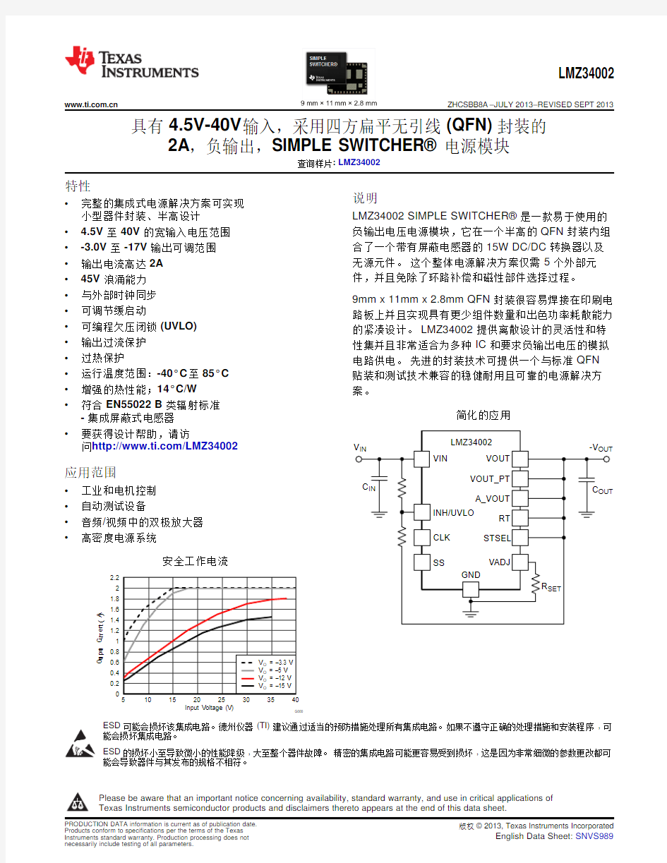
Safe Operating Current
The amount of output current that can safely be delivered by the LMZ34002depends on the input voltage and
the output voltage.Figure 33shows the maximum output current for four standard output voltages over input
voltage.
Figure 33.Safe Operating Current
F
F LMZ34002
https://www.doczj.com/doc/7315771181.html, ZHCSBB8A –JULY 2013–REVISED SEPT 2013
Application Schematics
Figure 34.Typical Schematic V IN =24V,V OUT =–12V
Figure 35.Typical Schematic V IN =12V,V OUT =–5V
()()-=W ??-+′?÷?÷è?UVLO2ON 3UVLO11.25R k V 1.250.910R ()UVLO130.5R k 2.910-=W ′LMZ34002
ZHCSBB8A –JULY 2013–REVISED SEPT https://www.doczj.com/doc/7315771181.html,
Input Voltage
The LMZ34002operates over the input voltage range of 4.5V to 40V.The maximum input voltage is 40V,
however,the sum of V IN +|V OUT |must not exceed 50V.
See the Undervoltage Lockout (UVLO)Threshold section of this datasheet for more information.
Undervoltage Lockout (UVLO)Threshold
At turn-on,the V ON UVLO threshold determines the input voltage level where the device begins power
conversion.R UVLO1and R UVLO2set the turn-on threshold as shown in Figure 36.The UVLO threshold is not
present during the power-down sequence.Applications requiring a turn-off threshold must monitor the input
voltage with external circuitry and shut-down using the INH control (see Output On/Off Inhibit (INH)).
The V ON UVLO threshold must be set to at least 4.5V to insure proper start-up and reduce current surges on the
host input supply as the voltage rises.If possible,it is recommended to set the UVLO threshold to
appproximantely 80to 85%of the minimum expected input voltage.
Use Equation 2and Equation 3to calculate the values of R UVLO1and R UVLO2.V ON is the voltage threshold during
power-up when the input voltage is rising.Table 4lists standard resistor values for R UVLO1and R UVLO2for
adjusting the V ON UVLO threshold for several input voltages.
(2)
(3)
Table 4.Standard Resistor Values to set V ON UVLO Threshold
V ON THRESHOLD (V)
4.5
5.0
6.58.09.010.015.020.030.0R UVLO1(k Ω)
174174174174174174174174174R UVLO2(k Ω)63.456.240.231.627.424.315.811.57.50
LMZ34002 https://www.doczj.com/doc/7315771181.html, ZHCSBB8A–JULY2013–REVISED SEPT2013
Power-Up Characteristics
When configured as shown in the application schematics,the LMZ34002produces a regulated output voltage following the application of a valid input voltage.During the power-up,internal soft-start circuitry slows the rate that the output voltage rises,thereby limiting the amount of in-rush current that can be drawn from the input source.The soft-start circuitry introduces a short time delay from the point that a valid input voltage is recognized.Figure37shows the start-up waveforms for a LMZ34002,operating from a12V input and the output voltage adjusted to–5V.The waveform were measured with a1.5-A constant current load.
Figure37.Start-Up Sequence
Light-Load Behavior
The LMZ34002is a non-synchronous converter.One of the characteristics of non-synchronous operation is that as the output load current decreases,a point is reached where the energy delivered by a single switching pulse is more than the load can absorb.This energy causes the output voltage to rise slightly.This rise in output voltage is sensed by the feedback loop and the device responds by skipping one or more switching cycles until the output voltages falls back to the set point.At very light loads or no load,many switching cycles are skipped. The observed effect during this pulse skipping mode of operation is an increase in the peak to peak ripple voltage,and a decrease in the ripple frequency.The amount of load current when pulse skipping begins is a function of the input voltage,the output voltage,and the switching frequency.
No-Load Operation
When operating at no load or very light load and the input voltage is removed,the output voltage discharges very slowly.If the input voltage is re-applied before the output voltage discharges,the slow-start circuit does not activate and the amount of inrush current is extremely large and may cause an over-current condition.To avoid this condition the output voltage must be allowed to discharge before re-applying the input voltage.Applying a 50-mA to100-mA minimum load helps discharge the output voltage.Additionally,monitoring the input voltage with a supervisor and shuting-down using the INH control(see Output On/Off Inhibit(INH))activates the internal slow-start circuit.
3.3 V
3.3 V LMZ34002
ZHCSBB8A –JULY 2013–REVISED SEPT https://www.doczj.com/doc/7315771181.html,
Switching Frequency
The recommended switching frequency of the LMZ34002is 800kHz.To operate at the recommended switching
frequency,connect the RT pin (Pin 30)to A_VOUT (at pin 32).
It is recommended to adjust the switching frequency in applications with both,higher input voltage (>18V)and
lower output voltage (<–8V).For these applications,improved operating performance can be obtained by
decreasing the operating frequency to 500kHz by adding a resistor,R RT of 93.1k Ωbetween the RT pin and
A_VOUT as shown in Figure 38.Figure 39shows the recommended switching frequency over input voltage and
output voltage.
Figure 38.R RT Resistor Placement Figure 39.Recommended Switching Frequency
Table 5.Standard Resistor Values For Setting Switching Frequency
f SW (kHz)
500800R RT (k ?)93.10(short)
Synchronization (CLK)
An internal phase locked loop (PLL)allows synchronization from 700kHz to 900kHz for 800kHz applications,or
400kHz to 600kHz for 500kHz applications.See Figure 39to determine switching frequency based on input
voltage and output voltage.To implement the synchronization feature,connect a square wave clock signal to the
RT/CLK pin with a duty cycle between 25%to 75%.The clock signal amplitude must transition lower than 0.5V
and higher than 2.2V.The start of the switching cycle is synchronized to the falling edge of RT/CLK pin.In
applications requiring CLK mode,configure the device as shown in Figure 40(800kHz)and Figure 41(500kHz).
Before the external clock is present,the device works in RT mode where the switching frequency is set by the
R RT resistor.When the external clock is present,the CLK mode overrides the RT mode.The first time the CLK
pin is pulled above the RT/CLK high threshold (2.2V),the device switches from RT mode to CLK mode and the
CLK pin becomes high impedance as the PLL starts to lock onto the frequency of the external clock.It is not
recommended to switch from CLK mode back to RT mode because the internal switching frequency drops to 100
kHz first before returning to the switching frequency set by the RT resistor.
Figure 40.CLK Configuration (800kHz Typ)
INH
Control
LMZ34002
https://www.doczj.com/doc/7315771181.html, ZHCSBB8A –JULY 2013–REVISED SEPT 2013
Output On/Off Inhibit (INH)
The INH pin provides electrical on/off control of the device.Once the INH pin voltage exceeds the threshold
voltage,the device starts operation.If the INH pin voltage is pulled below the threshold voltage,the regulator
stops switching and enters low quiescent current state.
The INH pin has an internal pull-up current source,allowing the user to float the INH pin for enabling the device.
If an application requires controlling the INH pin,an external level-shifter is required to interface with the pin
because in a positive-to-negative buck-boost supply,the INH pin is referenced to VOUT,not GND.Adding a
level-shifter (U1)as shown in Figure 42,allows the INH control to be refernced to GND.A recommended level-
shifter part #is DCX144EH-7from Diodes Inc.
Pulling the input of U1to GND applies a low voltage to the inhibit control pin and disables the output of the
supply,shown in Figure 43.Releasing the input of U1enables the device,which executes a soft-start power-up
sequence,as shown in Figure 44.The device produces a regulated output voltage within 10ms.The waveforms
were measured with a 1.5-A constant current load.
Figure 42.Typical Inhibit Control
Figure 43.Inhibit Turn-Off Figure 44.Inhibit Turn-On
LMZ34002
ZHCSBB8A –JULY 2013–REVISED SEPT https://www.doczj.com/doc/7315771181.html,
Slow-Start Circuit (SS)
Connecting the STSEL pin (Pin 29)to A_VOUT while leaving SS pin (Pin 28)open,enables the internal SS
capacitor with a slow-start interval of approximately 10ms.Adding additional capacitance between the SS pin
and A_VOUT increases the slow-start time.Figure 45shows an additional SS capacitor connected to the SS pin
and the STSEL pin connected to A_VOUT.See Table 6below for SS capacitor values and timing interval.
Figure 45.Slow-Start Capacitor (C SS )and STSEL Connection
Table 6.Slow-Start Capacitor Values and Slow-Start Time
C SS (nF)
open 101522SS Time (ms)10151720
Inrush Current
During turn-on,as the LMZ34002performs a slow-start sequence,an inrush current is induced as the output
capacitors charge up.The inrush current is in addition to the DC input current.The amount of inrush current
depends on the input voltage,output voltage and amount of output capacitance.Table 7shows the typical inrush
current for the input voltage,output voltage and the amount of output capacitance.Increasing the slow-start
capacitor reduces the inrush current by slowing down the ramp of the output voltage.See Slow-Start Circuit (SS).
Table 7.Typical Inrush Current
Output Capacitance →
100μF ceramic 200μF (1)320μF (1)430μF (1)VIN (V)VOUT (V)
Inrush Current (A)–3.3
0.10.10.10.1–5
0.10.20.20.35–12
0.30.8 1.2 1.8–15
0.4 1.3 2.5 3.6–3.3
0.10.10.10.1–5
0.10.10.10.212–12
0.20.40.60.8–15
0.30.50.9 1.3–3.3
0.10.10.10.1–5
0.10.10.20.224–12
0.20.20.30.5–15
0.30.30.50.7–3.3
0.20.20.20.236–5
0.20.20.20.2–12
0.20.30.40.4(1)This amount of capacitance includes the required 100μF of ceramic capacitance with additional bulk capacitance.
Sequence Analysis Software for Macintosh and Windows GETTING STARTED Introductory Tour of the LASERGENE System MAY 2001
DNASTAR, Inc. 1228 South Park Street Madison, Wisconsin 53715 (608) 258-7420 Copyright . 2001 by DNASTAR, Inc. All rights reserved. Reproduction, adaptation, or translation without prior written permission is prohibited,except as allowed under the copyright laws or with the permission of DNASTAR, Inc. Sixth Edition, May 2001 Printed in Madison, Wisconsin, USA Trademark Information DNASTAR, Lasergene, Lasergene99, SeqEasy, SeqMan, SeqMan II, EditSeq, MegAlign, GeneMan, Protean,MapDraw, PrimerSelect, GeneQuest, GeneFont , and the Method Curtain are trademarks or registered trademarks of DNASTAR, Inc. Macintosh is a trademark of Apple Computers, Inc. Windows is a trademark of Microsoft Corp. ABI Prism are registered trademarks of Pharmacopeia, Inc. Disclaimer & Liability DNASTAR, Inc. makes no warranties, expressed or implied, including without limitation the implied warranties of merchantability and fitness for a particular purpose, regarding the software. DNASTAR does not warrant, guaranty, or make any representation regarding the use or the results of the use of the software in terms of correctness, accuracy, reliability, currentness, or otherwise. The entire risk as to the results and performance of the software is assumed by you. The exclusion of implied warranties is not permitted by some states. The above exclusion may not apply to you. In no event will DNASTAR, Inc. and their directors, officers, employees, or agents (collectively DNASTAR) be liable to you for any consequential, incidental or indirect damages (including damages for loss of business profits, business interruption, loss of business information and the like) arising out of the use of, or the inability to use the software even if DNASTAR Inc. has been advised of the possibility of such damages. Because some states do not allow the exclusion or limitation of liability for consequential or incidental damages, the above limitations may not apply to you. DNASTAR, Inc. reserves the right to revise this publication and to make changes to it from time to time without obligation of DNASTAR, Inc. to notify any person or organization of such revision or changes. The screen and other illustrations in this publication are meant to be representative of those that appear on your monitor or printer.
F0/23B(C)、H3/36B、C7030电气系列 F0/23B(C)、H3/36B、C7030Electrical series 使 用 说 明 书 成都久和传动机械有限责任公司 地址:成都市双流县彭镇燃灯社区5组 电话(Phone):(028)67028807 传真(FAX):(028)85847360 邮编(ZIP code):610203
一.使用环境 1.周围空气温度 周围空气温度不超过+40℃,周围空气温度的下限为-25℃。且在24h周期内平均温度不超过+30℃。 2.海拔高度 安装地点的海拔不超过2000m。 3.大气条件 空气清洁,而其相对湿度在最高温度为+40℃,不超过50%,在较低温度时,亦允许有较大的相对湿度,如最湿月平均温度为+20℃,月平均最大相对湿度不超过90%,并注意因温度变化产生在产品表面的凝露。 4.供电电网质量 供电电网容量应保证满足塔机功耗,进线电压波动范围须保证不超过额定电压值的±10%。起升电控柜(L柜)适用于交流50Hz/380V、60Hz/440V三相电源。 5.安装条件 垂直安装倾斜度不超过5°;安装牢固,在主机工作过程中不会发生相对于主机的平移和垂直跳动;安装部位最高震动条件为:5~13Hz时,位移为1.5mm;13~15Hz时,震动加速度为1.0g。 二.阅读电气原理图的方法 1. 符号表示 各个部分字母表示见下列表格: a)操作,检测,指示
b) Ⅰ部分 c)Ⅱ或Ⅲ部分
d)方向或速度 2 . 工作顺序、工作原理及符号 不同的工作阶段用下面两种不同的形式表示: 在开关转换顺序中 A)在工作顺序示意图中,采用下面符号: 接触器或继电器进入“工作状态”:PV 接触器或继电器进入“停止状态”:PV PV表示两种工作状态。 B)在开关转换顺序中,采用下面符号: 接触器或继电器进入“工作状态”并通过同一机械或电气连锁保持:● 接触器或继电器进入“停止状态”:○ 3. 动作特性和各机构功能 F0/23B(C)、H3/36B、C7030等塔式起重机电气控制柜可工作在交流50Hz/380V、60Hz/440V的额定电压条件下。电气控制柜分A、L、HF柜,分别有供电,吊钩升降,小车变幅、回转几大系统。供电系统(A柜)供电源给塔机各机构的用电、并起电路的短路、过载保护作用。吊钩升降(L柜)控制塔机的吊钩起升、下降;小车变幅系统(HF柜)控制塔机的小车变幅(前后);回转系统(HF柜)控制塔机的回转。
IE安全漏洞及防范措施 摘要 谈到联网的计算机,就能想到它百纳海川的资讯,可以在网络的世界里找到自己想了解到的,自己想探索到的新知识,但是要想了解到这些资讯我们需要借助到一个工具,这就是我们每一个人都熟悉的----IE浏览器。技术的进步,离不开知识的传播。时代的需求就是我们的责任,我们要抓住信息时代的脉搏,在Internet飞速发展的今天,互联网成为人们快速获取、发布和传递信息的重要渠道,从而倍受人们的重视。互联网上信息的查找又要通过浏览器的浏览来实现,所以希望通过对IE浏览器的安全漏洞和防范措施的探讨让大家对网络及网络资源搜索的认识以及浏览器的各个功能。 关键词:IE浏览器/漏洞/措施
IE Security vulnerabilities and preventive measures ABSTRACT The PC is popular and the brilliant Computer-Culture is developing rapidly by drived of the Financial globalization,Assimilation of information and the Industrial knowledge-ization.Studying computer knowledge is becoming a consciousness action for many back-hoping people in the Boundary of the century.There are many progresses in the information industry,the time of the network and so on.We can see that more person's work and life are never left by a computer.It isn't left the spread of knowledge by technological progress.The demanding of the time is our responsibility.In the days of the internet developing fastly,we should catch the pulse of it,make the internet become a basilic channel that make people getting,issuancing and passing the news at a rapid rate.And then made the internet receives people's emphasis increasingly.One looking for the information by the browser's browsing,so I hope everyone should increasing Browser vulnerabilities and preventive measures and all kinds of functions of the browser by my paper. Keyword: Internet Explorer /vulnerabilities/measure
DMX512中文使用说明书 (2009-03-20 16:07:26) 转载 分类:灯光设备使用和技巧 标签: 灯光设备 一、四位数码管说明: XXXX *第一位代表CHASE,共有6个 *第二位代表SCENSE,共有8个 *第三四位代表BANK,共有30个 *设置MIDI通道时第三四位代表MIDI通道,共有16个MIDI通道 *一个CHASE最多可以包含240个SCENSE *一个BANK最多可以包含8个SCENSE *一个SCENSE最多可以包含192个通道(也可以说是12个SCANNER) SCANNER1:通道1~通道16 SCANNER2:通道17~通道32 以此类推 SCANNER12:通道181~通道192 *一个SCANNER最多可以包含16个通道 *调节滑杆时显示数值或者百分比 二、操作时请注意数码屏的指示灯在什么状态。 *BLANKOUT *STEP *PROGRAM *MUSIC TIGGER *AUTO TIGGER 三、DMX512面板功能说明 1、SCANNERS 按下SCANNER键,其旁边的LED灯亮,其中连接8个通道的输出可被调节,在SCENS运行时,如果可调电位器控制为OFF,则调节电位器不会影响通道输出,但如果可调电位器控制为ON,则通道输出会随相应的可调电位器的改变而改变; 2、SCENS按健 按下一个SCENS键可触发SCENS或存入一个SCENS,第二个数码管头显示SCENS1-8; 3、可调电位器 调节可调电位器改变DMX的通道输出大小,最小是0最大为255或者从0%-100%,可调电位器1-8控制连续的八个通道;
4、PAGE/SELECT键 选择PAGE A或PAGE B,PAGE A为每个SCANNER的前八个通道PAGE B为每个SCANNER的后八个通道 5、SPEED SLIDER 推动这个推杆调整走灯速度; 6、FADE TIME SLIDER 推动这个推杆调整FADE TIME; 7、LED DISPLAY 8、BANK按键(↑/↓) 第三位和第四位数码管显示BANKS(01-30),按下↑/↓键,BANK增大或减小,显示的SCENS为该BANK里的SCENS; 9、CHASE 1-CHASE 6键 用于CHASES编程或CHASES运行的选择; 10、PROGRAM键 上电本机在走动运行状态,按下PROGRAM键盘2秒,编程指示灯闪动可编程SCENSR和CHASER,再按下PROGRAM键2秒,编程指示灯灭回到运行状态; 11、MIDI/ADD键 A、在运行状态按住MIDI键2秒,第3及第4位数码管闪动,通过↑或↓选择MIDI通道,再按MIDI键2秒结束MIDI通道的设置选择的MIDI通道被存贮;或者除↑/↓键以外的任何键都可结束MIDI通道的设置,不存贮所选取的MIDI通道; B、在编程状态,用于编辑; 12、AUTO/DEL键 A、在运行状态,按下AUTO/DEL键,自动触发指示灯亮,表示在自动触发状态,再按下AUTO键退出自动触发状态,自动触发指示灯灭; B、在编程状态,用于SCENS及CHASE编程; 13、MUSIC/BANK COPY键 A、在运行状态,按下MUSIC键,声音触发指示灯亮,可由声音触发SCENS,再按一下MUSIC键,声音触发指示灯灭,退出声音触发状态; B、在编程状态,用于SCENS及CHASE编程;
1.文件目录结构 \app-- APs构建环境 \bin --可执行二进制APs和windows链接库 \data-- APs样本数据 \doc --文档文件 \lib --库生成环境 \src --RTKLIB库的源程序 \test--测试程序和数据 \util-- 实用程序工具 2.\bin\rtklaunch.exe 应用程序启动器 3.RTKNAVI实时定位结算 输入GPS / GNSS接收机原始观测数据,实时进行导航处理。 3.1执行\bin\rtknavi.exe
3.2用RTKNAVI进行实时定位必须输入GPS/GNSS接收机原始观测数据和卫星星历,点击I进入输入流对话框 检查设置Rover、Basestation、Correction三个选项的设置,如果设 置定位模式,只选择一个,基站和校正并不需要。 流类型可有从以下选项中选择 (a)Serial :串口输入数据 (b)TCP Client :连接到一个TCP服务器,通过TCP连接输入数 据 (c)TCP Server :接受一个TCP客户端连接和通过TCP连接的输 入数据 (d)NTRIP Client :连接一个NTRIP caster输入数据 (e)File :日志文件中输入数据。[.conf] (f)FTP :通过FTP下载一个文件后输入数据 (g)HTTP :通过(a) HTTP 下载一个文件后输入数据 3.3选择流类型为?Serial?(连续的)点击...按钮设置选项
3.4在流类型中如果你选择了SerialTCP Client或者TCP Server作为类型,你可以通过流设置GPS / GNSS接收机启动和关闭命令,设置命令,按下“Cmd?标签下的…按钮。在?Serial/TCP Commands?对话框中进行设置,可以加载和保存命令 3.5流类型中设置类型为?File?可以设置文件输入路径,数据为原始数据,还可以设置时间 3.6设置输出流格式,点击O按钮,弹出 ?Output Streams?对话框,设置类型,
11.6 疑难解答 危险: 严格遵守11.1章中“危险”一节的要求。 警告: 在(废料)切割器或者料盘分隔板附近工作时不论何时都必须戴厚度适度的保护手套。不论(废料)切割器及料盘分隔板刀片处于固定还是可动状态,甚至贴片机已经断电,都存在高风险的受伤可能性。 严禁从下方进入气压切割装置或者从上方进入空的皮带供料器,甚至是为了解决问题(如供料器卡住时)。 11.6.1 更换气压切割刀片 警告: 佩戴厚度适度的保护手套。 取出刀片时,只能捏住它的外面,左边和右边。 严禁将刀片放置身体上,例如,放到膝盖或者腿上。 不要将脚放到刀片上。你可能会重伤自己或者至少将衣服划破。 拆除刀片后确保没人会因踩到刀片伤到他们自己。 11.6.1.1 移除刀片 运行贴片机,开启压缩空气系统。 中断贴片机菜单中可动器件,然后将它取出。 停止运行贴片机,切断总电源,然后关闭压缩空气。开启位于压缩空气单元的针状阀以使压缩空气流动(查看11.1章中“危险”一节)。 松弛螺丝更换喷嘴,略微将它举起并保持它在这一位置。 拔下电缆和喷嘴气动软管 慢慢的拔出喷嘴。 拧下空供料器各个配件的螺丝(参考图11.4.1 -> 11, 9),然后将这些管道移出机器。 警告: 刀片的刀刃处始终可能伤到你自己。 基于这一原因,挡板、顶盖及保护罩(参见图11.4.3 -> 6,7, 2)必须安装到位。 打开连接电缆顶盖(见图11.6.6 -> 5) 拧下位于连接线缆(见图11.6.6 -> 5)处的气压连接阀(Y型插座:见图11.6.3 -> 9) 拔下电源和控制面板插头插座。(见图:see Fig. 11.6.5 -> 11, 10) 仔细解开外部控制面板箱内(见图11.6.5 -> 15)对应的接线头(向左或者向右)。在此期间不要损坏连线。 将顶盖放回控制面板及连接线缆处。 取出供料器斜槽(它只是扣住而已)。这使得取下刀片变得容易。 警告: 刀片下方必须保持干净。(例如,不要把脚放到下面) 在贴装元器件情况下松弛位于贴片机左右两个侧面的缓冲部件(2头M8六角头两边螺钉,见图 11.4.1 -> 15)。
< >内为需要输入的内容,但不包括括号。所有命令都需要在MrBayes >的提示下才能输入。 文件格式: 文件输入,输入格式为Nexus file(ASCII,a simple text file,如图): 或者还有其他信息: interleave=yes 代表数据矩阵为交叉序列interleaved sequences nexus文件可由MacClade或者Mesquite生成。但Mrbayes并不支持the full Nexus standard。 同时,Mrbayes象其它许多系统软件一样允许模糊特点,如:如果一个特点有两个状态2、3,可以表示为:(23),(2,3),{23}或者{2,3}。但除了DNA{A, C, G, T, R, Y, M, K,S, W, H, B, V, D, N}、RNA{A, C, G, U, R, Y, M, K, S, W, H, B, V, D, N}、Protein {A, R, N, D, C, Q, E, G, H, I, L, K, M, F, P, S, T, W, Y, V, X}、二进制数据{0, 1}、标准数据(形态学数据){0, 1, 2, 3, 4, 5, 6, 5, 7, 8, 9}外,并不支持其他数据或者符号形式。 执行文件: execute
目录 一:拉伸薄膜缠绕包装机 (2) 二:主要技术参数 (2) 三:产品保修 (3) 四:拆箱、安装、调试 (3) 五:控制板操作说明 (5) 六:设备维护 (7) 七:使用 (9) 八:功能使用及其它 (9) 8-1、记数误差10 8-2、光电开关的使用10 8-3、薄膜操作简图11 8-4、预拉伸薄膜导出11 8-5、可移动限位块11 8-6、薄膜拉伸12 九:使用安全 (13) 附设备可能出现的故障及排除方法 电气原理图
一:拉伸薄膜缠绕包装机 1. 拉伸薄膜缠绕包装机是以LLDPE拉伸薄膜为包装材料,对多种货 物进行裹包的专业包装机器。 2. 使用我公司出品的系列薄膜缠绕拉伸包装机器,可以降低包装成 本,方便存储与运输,易于对包装材料(薄膜)进行回收,减少环境污染。这是一种现今较普遍流行的绿色运输包装方式之一。 3. 这种包装方式已经广泛应用于玻璃制造业、纸业、化工业、机械 制造业、食品业等各种不同行业,特别是在出口贸易货物运输中的集装箱已经得到广泛的应用。 4. 我公司出品全面的拉伸薄膜裹包机,除托盘基本型外,还出品圆 筒纸/帘子布型,线缆型,水平型、圆筒径向包装等多种机型。另外我们还出品牛皮纸、珍珠棉、普通PE膜等裹包机,如有需要请向我们的销售部门索取更详尽的说明和资料。 二:主要技术参数 1.包装规格: 型号最大货高(mm)最大托板尺寸(mm) TP1650F-L 2000 1200╳1200 2.承重:≤2000 kg 3.使用包装材料: 材料宽度厚度膜卷内芯孔膜卷外径LLDPE拉伸膜500 mm 17-35μm76.2mm(3英吋) ≤280 mm 4.工作电源:AC220V/50HZ 20A -1p。 务必使用单独固定电源,严禁使用临时线或与其他设备合用电源,电压不得低于200V,或高于250V,接线时请核对火线零线和地线(因电源不正确引起的电气损坏和其他损坏不在保修之
望远镜用户指南
概览............................................... (5) 关于本指南 望远镜 概观 按钮 手势 最多显示头---(HUD)的 工具和手段 入门................................................ (17) 版本和功能 硬件和软件兼容性说明............................................. (17) 启用定位服务 设置最多望远镜 开始标记和跟踪对象............................................. . (22) ViewVinder ................................................. . (23) 设置颜色 设置最多的HUD 快速切换 HUD的操作模式 缩放 指南针................................................. (28) 校准
增强现实和三维罗盘............................................. .. (29) 寻找目标对象 设置最多罗盘 罗盘定位模式............................................... .. (32) 罗经................................................. .. (34) 开始使用罗经............................................... .. (34) 确定启动轴承............................................... .. (35) 漂移和调整 全球定位系统................................................. . (37) 设置最多的GPS 获取GPS数据 设置单位 查找................................................. .. (39) 概观 按钮 快速目标标记 添加目标 管理目标 寻找和跟踪 在地图上观测地点的目标............................................. .. (47) 跟踪................................................. .. (48) 设置跟踪
MAXIDRIVER3.4数字音频处理器 ALTO MAXIDRIVER3.4数字处理器是集增益、噪声门、参数均衡、分频、压缩限 幅、延时为一体的全功能数字音频处理器,具有2个输入通道和6个输出通道,本机内设10种工厂预设的分频模式,64个用户程序数据库位置以及利用多媒体卡(MMC)进行128个用户程序外置储存的功能。MAXIDRIVER3.4是新一代全数字音 频处理器,采用分级菜单形式,操作非常方便。 功能键介绍 前面板 1、MODE---分级菜单选择,按动时循环选择PRESET(预设)、DELAY(延时)、EDIT(编辑)、UTILITY(系统设置)菜单功能。同时相对应的LED指示灯会被点亮。这时可以进入所选择的菜单进行参数编辑。 2、LED指示灯---当你用MODE键选择需要编辑的菜单时,相对应的LED指示 灯会被点亮。 3、2X16位LCD显示屏---显示正在编辑或查看的系统参数或系统状态。 4、数据轮---转动这个数据轮可以调节需要编辑的参数的数值,顺时针旋转提高数值,逆时针旋转减低数值。 5、PREV/NEXT---前翻/后翻键,每个主菜单下面都有若干个子菜单,通过按动这两个按键可以向前或向后选择所需要进行编辑的子菜单。 6、NAVIGATION CURSOR KEYS---光标移动键,每个子菜单中都有若干个可以 编辑的参数选择,按动这两个键,可以选择需要编辑的参数,选中的参数会闪烁。 7、CARD---储存卡插入口,在这个插口插入MMC储存卡,利用PRESET(预设) 菜单下,可以对该储存卡进行写入、读出等操作。 8、ENTER---确认键,按此键可以对所选择的菜单或编辑的参数数值进行确认。 9、ESC---取消键,按此键可以对所选择的菜单或编辑的参数数值进行取消操作,返回上一级菜单。 10、输入电平指示表,实时指示A/B两个输入通道输入电平的强弱数值。 11、MUTE---静音按键,按下后将关闭相应输出通道的输出信号,相对应的 红色LED指示灯将点亮。 12、输出电平指示表,显示每个输出通道输出电平大小数值,这里显示的数 值不是绝对的输出电平数值,而是与该列LED指示灯中的LIMIT(限幅)指示为基础相比较的数值。
用户使用说明
目录 1.手机外观和按键说明2.使用手机存储卡做为U盘3.WLAN 4.蓝牙 5.电子邮件 GMAIL 电子邮件 6.拨号 7.信息 8. 通讯录 9. 浏览器 10.录音机 11.时钟 12.计算器 13.相机 相机 摄像机 14.图库 15.音乐 16.日历 17.收音机 18. 设置 19. 手机使用注意安全
1 .手机外观和按键说明 在任何的应用程序或界面上,按下此键可返回首页界面。 按下此键可开启动作清单,让您在目前的界面或选项菜单中执行动 作。 按下此键可返回前一个界面,或是关闭对话框、选项菜单、通知面板 或屏幕键盘。 按住此键可开启电话的选项菜单,然后您可以选择要锁定屏幕、关闭 手机,或将手机设成静音模式。 按此键可以增大音量。 按此键可以减小音量。 静音状态时按此键可以将手机调为振动状态。 进入相机界面,可切换至前摄像头自拍 2.使用手机存储卡做为U盘 若要从计算机传送音乐、相片和其它档案到您的储存卡,您必须先将手机储存卡设成U盘。
将手机储存卡设成U盘 1)选择“USB已连接”,可以装载U盘,可将音乐、相片和其它档案到您的储存卡或内置存储卡中。 2)选择“作为USB存储设备使用”可以打开右边的选项。 具体如下图所示: 3:有截图会显示的状态栏 3)插入SD卡。 打开USB连接。1 2 3 4 5 1:USB已连接电脑(当连接360手机助手)2:作为USB存储设备使用 4:已连接到 USB调试 5:已连接USB
3)连接后可以直接在PC端查看相机拍摄的图片 ?注意:不同的个人电脑操作系统如何操作正常使用U盘。 1)这个主题可以直接使用 2)xp更新windows媒体播放器到11 3)安装wpdmtp。inf司机 4)vista未经证实的 ?注意:在个人电脑业务助理工具如手机,必须打开USB调试。 WLAN提供最远300英尺(100M)的无线网络接入范围。若要使用手机上的WLAN,您必须连接到无线接入点或「热点」。 注意:WLAN信号的可用性与涵盖范围需视数量、基础结构,以及其它信号穿透的对象而定。 开启WLAN并连接到无线网络 1)按下首页>菜单,然后触碰设置 2)在无线和网络下。点击WLAN开关按钮,以开启WLAN。手机会自动扫描可用无线网络。 3)触碰WLAN,进入WLAN设置。接着WLAN网络列表会显示查找到的WLAN网络的网络名称和安全性设置(开 放网络或以WEP、WPA/WPA2加密)。默认启用WLAN高级设置中的网络通知,手机会在查找到有可用的 开放无线网络时在状态栏显示图标。 4)触碰其中一个WLAN网络,以进行连接。当您选取开放网络时,手机会自动连接到该网络。如果选取的 是WEP、WPA/WPA2加密网络,则必须先输入相应的密码,然后再触碰连接。 注意:当手机连接到无线网络后,状态栏会显示
Vector NTI 7.0 User's Manual 软件包中文翻译者:宋厚辉(浙江大学) 前言(Introduction) 1.程序附带的数据库(Vector NTI database)包括:DNA/RNA、蛋白质、内切酶、寡核苷 酸、凝胶mark。此外程序还提供数据库开发(Database Explorer)功能,用户可以自己修改、添加、拷贝感兴趣的各类数据库。 2.创建新分子(有四种方法) A.用GenBank/GenPept, EMBL/SWISS-PROT and FASTA、ASCII等格式输入DNA 或氨基酸。 B.手工粘帖,然后保存到数据库中 C.从其他分子、接头、载体中剪切、拼接构键 D.从DNA或RNA分子的编码区翻译成蛋白质 3.关于新分子的序列特征图谱:利用GenBank/GenPept, EMBL/SWISS-PROT or FASTA等 格式输入的分子都能显示出序列和结构图,但自己手工粘帖的没有,需要自己编辑 第一章Chapter 1 Tutorial: Display Windows(显示窗口) 目的:创建显示窗口,并对图、序列和文本进行操作 ? 1.登录Vector NTI 安装后首次登录,系统将提示是否允许填充空库,点OK。这样DNA molecules, proteins, enzymes, oligos, and gel markers将组成NTI的数据库。并出现下列两个窗口。 ? 2. 观察出现的Vector NTI 工作窗口和Database Explorer窗口
上面的第一个窗口为工作窗口,由菜单栏和工具条两栏,移动鼠标到工具栏任意选项处,鼠标自动显示每个工具条的功能。 第二个窗口为exlporing——local vector NTI database,显示的是上次打开的DNA/RNA或蛋白分子。 3. Create a Display Window for pBR322 激活exlporing——local vector NTI database窗口中的DNA/RNA Molecules (MAIN) 数据库,找到pBR322分子并双击打开。显示如下窗口:
Pierce? Co-Immunoprecipitation (Co-IP) Kit(26149) 中文说明书 介绍: Thermo 公司的Pierce?免疫共沉淀试剂盒,可通过将铆钉抗体固定在琼脂 糖支撑物上,从裂解液中或其他复杂混合物中,分离出天然蛋白复合物。Co-IP 是一种研究蛋白与蛋白相互作用通用的方法,该方法使用一种诱饵蛋白与抗原 进行免疫沉淀反应,然后可通过免疫共沉淀任何与诱饵蛋白具有相互作用的猎 物蛋白。传统的Co-IP方法使用蛋白A或G共同洗脱抗体的重链和轻链,这很 可能导致将相关的蛋白一起洗脱下来,掩盖一些重要的结果。Pierce?免疫共沉 淀试剂盒通过将共价结合抗体固定在一个胺类活性反应树脂上解决了这一问题。该试剂盒包含足够的用于蛋白结合和恢复的缓冲液,完成对照试验的高校离心 柱和收集管,这些产品进一步缩短了操作实验的时间。 重要产品信息: 略 Co-IP实验步骤: A.抗体固定 注意:以下试验步骤是针对用无胺和其他载体蛋白稀释的10-75μg亲和纯 化抗体(参考重要产品信息一节)。根据实际使用比例参考这一协议步骤。参 考重要产品信息节表1中的建议抗体用量和树脂体积用量。 1.室温平衡胺连接耦合树脂(AminoLink?Plus Coupling Resin)和试剂; 2.为每个Co-IP反应准备2ml 1×Coupling Buffer(超纯水稀释20×Coupling Buffer);
3.轻轻涡旋混匀装有AminoLink?Plus Coupling Resin的瓶子,使其处于悬浮状态。使用大口径(或剪掉一段枪头端),添加50μl树脂悬液到Pierce提供的离心柱中,将离心柱放入微量离心管中,1000g离心1min,弃滤液; 4.添加200μl 1×Coupling Buffer 清洗树脂2次,离心弃滤液; 5.将离心柱放于纸巾上,轻巧离心柱底部,去除剩余的液体,插上底塞; 6.准备10-75μg亲和纯化抗体用于结合蛋白,调整体积至200μl,使用足够的超纯水和20×Coupling Buffer来制备1×Coupling Buffer。例如:添加10μl 20×Coupling Buffer,180μl超纯水和10μl浓度为1μg/μl。可直接添加含有超纯水、20×Coupling Buffer、亲和纯化抗体的树脂在离心柱中。 7.在通风厨中,每200μl反应体系,添加3μl氰基硼氢化钠溶液; 注:氰基硼氢化钠属剧毒物质,操作时要小心并穿戴防护服。 8.拧紧离心柱上螺帽,室温涡旋孵育90-120min,确保浆体在孵育过程中处于悬浮状态; 9.握紧底塞,拧开并拿走螺帽,将离心柱置于收集管中离心,保存滤液以便验证抗体耦合; 10.打开螺帽,添加200μl 1×Coupling Buffer,离心弃滤液,重复此步骤1次; 11. 向离心柱中添加200μl Quenching Buffer,离心弃滤液; 12. 将离心柱放于纸巾上,轻巧离心柱底部,去除残留液体,插上底塞。在树脂上添加200μl Quenching Buffer; 13. 在通风厨中,添加3μl氰基硼氢化钠溶液,拧紧螺帽;轻轻摇动并孵育15min; 14.取出底塞,拧开螺帽,将离心柱置于一收集管中,离心弃滤液; 15.打开螺帽,采用200μl 1×Coupling Buffer洗脱树脂,离心。再次重复此步骤; 16.用150μl Wash Solution洗脱树脂6次,每次洗脱后离心; 17.不管是进行细胞裂解、Co-IP,还是储存树脂,都需要继续进行下列步骤; 18.用200μl 1×Coupling Buffer洗脱树脂2次,每次需离心;
本程序用来绘制发表质量的质粒图,可广泛应用与论文、教材的质粒插图。其特性包括: ●知道序列或不知序列结构均能绘制质粒图 ●可读入各种流行序列格式文件引入序列信息。 ●自动识别限制位点 ●可构建序列结构,功能包括:从文件插入序列、置换序列、序列编辑、部分序列删 除等。 ●绘图功能强大,功能包括:位点标签说明、任意位置文字插入、生成彩图、线性或 环形序列绘制、可输出到剪贴板、可输出到图像文件。 ●限制酶消化分析报告输出与序列输入报告功能。 1. 不知序列结构绘制质粒图 从菜单或工具栏选择File New,出现一个空白文件,再在菜单或工具栏选择Insert Blank,出现一个对话框,如下: 输入质粒标题与碱基对数,选择为线性或环形序列,单击OK键,便出现质粒图,可继续进行编辑,但因为不知其序列,所以有一些功能无法进行。 2. 从一个GenBank文件建立一个质粒图 选择File New后,在菜单或工具条中选择Insert GenBank File,便打开对话框,由你选择一个指定文件,确定后,便根据此序列生成质粒图,进行进一步编辑。 3. 从一个其它序列格式文件建立质粒图 选择File New后,在菜单或工具条中选择Insert Sequence File,便打开对话框,由你选择一个指定文件,确定后,便根据此序列生成质粒图,进行进一步编辑。支持的序列格式包括:Stanford, NRBF, EMBL, Fasta, GCG, DNAStrider, Fitch, Pearson, Zuker, Olsen, Phylip, ASXII/RAW, PIR, CODA TA, MSF, DNAStar,若是多序列文件,将由你选择哪一条序列进行作图。 4. 标记限制酶切位点 菜单或工具条中中选择Restriction Enzymes命令,用来标记目前序列中发现的限制酶切位点。出现以下窗口:
XK3190-A27E型称重显示指示器 V1.02 上海耀华称重系统有限公司制造
目录 第一章技术参数........................................ - 2 - 第二章安装连接........................................ - 3 - 一、仪表示意图............................................ - 3 - 二、传感器的连接.......................................... - 3 - 三、串行通讯接口与大屏幕.................................. - 4 - 第三章操作说明........................................ - 5 - 一、开机.................................................. - 5 - 二、按键操作说明.......................................... - 5 - 三、称重操作.............................................. - 5 - 第四章标定说明........................................ - 7 - 第五章用户功能设置..................................... - 8 - 第六章信息提示出错说明 ............................... - 10 - 第七章蓄电池的使用 ................................... - 10 - 亲爱的用户: 在使用仪表前,敬请仔细阅读说明书!
Pajek 分析和可视化大型网络的程序 参考手册 List of commands with short explanation version 1.16 Vladimir Batagelj and Andrej Mrvar 翻译:先红、一生有我、傻大师、沧海回眸、AndyChang、comp network、遥遥、大头、三叶草 整理:饭团 Ljubljana, October 4, 2006 1996, 2006 V. Batagelj, A. Mrvar. Free for noncommercial use. PdfLaTex version October 1, 2003
Vladimir Batagelj Department of Mathematics, FMF University of Ljubljana, Slovenia http://vlado.fmf.uni-lj.si/ vladimir.batagelj@fmf.uni-lj.si Andrej Mrvar Faculty of Social Sciences University of Ljubljana, Slovenia http://mrvar.fdv.uni-lj.si/ andrej.mrvar@fdv.uni-lj.si
目录 1.Pajek介绍 (1) 2.数据对象 (3) 3 主窗口工具栏 (7) 3.1 File(文件) (7) 3.2 Net(网络) (11) 3.3 Nets(网) (26) 3.4 Operation(操作) (28) 3.5 Partition(分类) (34) 3.6 Partitions(分类) (35) 3.7 Vector(向量) (35) 3.8 Vectors(向量) (36) 3.9 Permutation(排序) (37) 3.10 Cluster(类) (37) 3.11 Hierarchy(层次) (37) 3.12 Options(选项) (38) 3.13 Info(信息) (40) 3.14 Tools(工具) (40) 4 绘图窗口工具 (42) 4.1 主窗口绘图工具 (42) 4.2 Layout(布局) (42) 4.3 Layers(图层) (43) 4.4 GraphOnly(仅图形) (44) 4.5 Previous(退回到前一次操作) (44) 4.6 Redraw(重绘) (44) 4.7 Next(下一步) (44) 4.8 Options(选项) (45) 4.9 Export (导出) (47) 4.10 Spin(旋转) (49) 4.11 Move(移动) (49) 4.12 Info (信息) (49) 5 Exports to EPS/SVG/VRML (50) 5.1 Defaults (默认值) (50) 5.2 Parameters in EPS,SVG and VRML Defaults Window(在EPS/SVG/VRML默认窗口中 的参数) (50) 5.3 Exporting Pictures to EPS/SVG — 在输入文件中定义参数 (52) 6 在Pajek中使用Macros(宏) (57) 6.1 什么是Macro(宏)? (57) 6.2 怎样标明一段宏? (57) 6.3 如何运行宏? (57) 6.4 例子 (57) 6.5 重复最后的命令 (57) 附加信息 (59)