STM8S做IAP
- 格式:docx
- 大小:52.23 KB
- 文档页数:3
November 2012Doc ID 14153 Rev 41/25AN2659Application noteSTM8 in-application programming (IAP)using a customized user-bootloaderIntroductionThis application note is intended for STM8 firmware and system designers who need to implement an in-application programming (IAP) feature in the product they are developing with the STM8 microcontroller.The STM8 is an 8-bit microcontroller family with a Flash memory for storing the user program code or firmware. IAP makes it possible to update the firmware ‘in situ’, after the microcontroller has been embedded in the final product. The advantage is that the microcontroller board can stay inside its product enclosure. No mechanical intervention is needed to make the update.IAP is extremely useful for distributing new firmware versions. It makes it easy to add new product features and correct problems throughout the product life cycle.The user-bootloader firmware source code provided with this application note shows an example of how to implement IAP for the STM8 microcontroller. Use this code as a reference when integrating IAP in your STM8 application. It includes the following features:●Bootloader activated by external pin (jumper on PCB)●Flash block programing by executable RAM code management ●Read while write (RWW) feature ●High level C-language usage ●Reduced size of the code (optimized code) ●Support for multiple communication interfaces (SPI, I 2C, and UART)●UART code compatible with ST Flash loader demonstrator software Table 1.Applicable productsProduct family Part numbersMicrocontrollers –STM8S003xx, STM8S005xx, STM8S007C8–STM8S103xx, STM8S903xx, STM8S105xx, STM8S207xx, STM8S208xx,–STM8AF6x26/4x/66/68, STM8AF5xxx, STM8AF6x69/7x/8x/9x/Ax–STM8L05xxx–STM8L101xx–STM8L151C2/K2/G2/F2 and STM8L151C3/K3/G3/F3–STM8L151x4, STM8L151x6, STM8L152x4, STM8L152x6–STM8L151x8, STM8L152x8, STM8L151R6, STM8L152R6, STM8L162R8,STM8L162M8–STM8AL313x, STM8AL314x, STM8AL316x, STM8AL3L4x, STM8AL3L6x–STM8TL5xxx Contents AN2659Contents1Operation theory . . . . . . . . . . . . . . . . . . . . . . . . . . . . . . . . . . . . . . . . . . . . 52STM8 devices with built-in ROM-bootloader . . . . . . . . . . . . . . . . . . . . . 62.1Implementation details . . . . . . . . . . . . . . . . . . . . . . . . . . . . . . . . . . . . . . . . 62.2Adapting IAP master side to ROM-bootloader protocol . . . . . . . . . . . . . . . 73User-bootloader for STM8 devices . . . . . . . . . . . . . . . . . . . . . . . . . . . . . 83.1User-bootloader firmware example description . . . . . . . . . . . . . . . . . . . . . 93.2Configuring the user-bootloader firmware example . . . . . . . . . . . . . . . . . 124Memory management for IAP . . . . . . . . . . . . . . . . . . . . . . . . . . . . . . . . . 134.1Memory protection . . . . . . . . . . . . . . . . . . . . . . . . . . . . . . . . . . . . . . . . . . 134.1.1Flash memory protection . . . . . . . . . . . . . . . . . . . . . . . . . . . . . . . . . . . . 134.1.2User boot code protection (UBC) . . . . . . . . . . . . . . . . . . . . . . . . . . . . . . 134.1.3Vector table redirection . . . . . . . . . . . . . . . . . . . . . . . . . . . . . . . . . . . . . 144.2Block versus word programming . . . . . . . . . . . . . . . . . . . . . . . . . . . . . . . 154.3RAM versus Flash programming code location . . . . . . . . . . . . . . . . . . . . 154.3.1Programming the data EEPROM area . . . . . . . . . . . . . . . . . . . . . . . . . . 154.4Library support for Flash programming . . . . . . . . . . . . . . . . . . . . . . . . . . 164.4.1Flash programming function list . . . . . . . . . . . . . . . . . . . . . . . . . . . . . . . 165Configuring the Cosmic compiler for RAM code execution . . . . . . . . 185.1Creating a segment in the STVD project . . . . . . . . . . . . . . . . . . . . . . . . . 185.2Creating a memory segment in the Cosmic linker file . . . . . . . . . . . . . . . 195.3Finishing and checking the configuration . . . . . . . . . . . . . . . . . . . . . . . . . 20 6Setting up your application firmware for user-bootloader use . . . . . . 227Conclusion . . . . . . . . . . . . . . . . . . . . . . . . . . . . . . . . . . . . . . . . . . . . . . . . 237.1Features in the final user-bootloader application . . . . . . . . . . . . . . . . . . . 23 8Revision history . . . . . . . . . . . . . . . . . . . . . . . . . . . . . . . . . . . . . . . . . . . 242/25Doc ID 14153 Rev 4AN2659List of tables List of tablesTable 1.Applicable products . . . . . . . . . . . . . . . . . . . . . . . . . . . . . . . . . . . . . . . . . . . . . . . . . . . . . . . 1 Table 2.Document revision history . . . . . . . . . . . . . . . . . . . . . . . . . . . . . . . . . . . . . . . . . . . . . . . . . 24Doc ID 14153 Rev 43/25List of figures AN2659 List of figuresFigure 1.Typical bootloader application . . . . . . . . . . . . . . . . . . . . . . . . . . . . . . . . . . . . . . . . . . . . . . . 5 Figure 2.Example of STM8S208xx bootloader. . . . . . . . . . . . . . . . . . . . . . . . . . . . . . . . . . . . . . . . . . 6 Figure 3.Example of user-bootloader implementation in the Flash memory. . . . . . . . . . . . . . . . . . . . 8 Figure 4.Example of the user-bootloader package provided . . . . . . . . . . . . . . . . . . . . . . . . . . . . . . . 9 Figure 5.Bootloader flowchart. . . . . . . . . . . . . . . . . . . . . . . . . . . . . . . . . . . . . . . . . . . . . . . . . . . . . . 11 Figure er boot code area and user application area . . . . . . . . . . . . . . . . . . . . . . . . . . . . . . . . . 14 Figure 7.Define linker memory section in STVD. . . . . . . . . . . . . . . . . . . . . . . . . . . . . . . . . . . . . . . . 19 Figure 8.Setting the project start and vector table addresses in STVD . . . . . . . . . . . . . . . . . . . . . . 22 4/25Doc ID 14153 Rev 4AN2659Operation theory Doc ID 14153 Rev 45/251 Operation theoryIn practice, IAP requires a bootloader implemented in the STM8 firmware that cancommunicate with an external master (such as a PC) via a suitable communicationinterface. The new code can be downloaded into the microcontroller through this interface.The microcontroller then programs this code into its Flash memory.IAP can also be used to update the content of the internal data EEPROM memory, and theinternal RAM memory.This operation is useful when a microcontroller is already soldered in its final application andneeds a firmware update.Figure 1 shows a typical bootloader application.Figure 1.Typical bootloader applicationThe bootloader is that part of the code which runs immediately after a microcontroller resetand which waits for an activation signal (for example, from grounding a specific pin orreceiving a token from a communication interface). If activation is successful the code entersbootloader mode. If activation fails (for example due to a timeout or the jumper on the pin notbeing present) the bootloader jumps directly to the user application code.In bootloader mode, the microcontroller communicates with the external master devicethrough one of the serial communication interfaces available in it (UART, SPI, I 2C, CAN)using a set of commands. These commands are usually:●Write to Flash ●Erase Flash ●Verify Flash ●Additional operations such as read memory and execute code from a given address (jump to given address).The ST proprietary bootloader can be used. It is embedded in the ROM memory of STM8devices with a program memory greater than 8 Kbytes. In this case, no code development isneeded. To use the proprietary bootloader, enable it via the option bytes.Alternatively, develop a customized bootloader using, for example, a serial communicationinterface that is not supported in ST versions or in devices where the ST bootloader is notpresent. Such a bootloader should be stored in the user boot code area (UBC) in themicrocontroller. This guarantees protection against unintentional write operations.RS232RS232/TTLconverterSTM8 boardSTM8Bootloader enable PC jumper2 STM8 devices with built-in ROM-bootloaderMost STM8 devices have an internal bootROM memory which contains an ST proprietarybootloader. Consequently, they already have a built in IAP implementation (see UM0560:STM8 bootloader).details2.1 ImplementationThe built-in ROM-bootloader is located in a dedicated part of the memory called theBootROM. The ROM-bootloader code is fixed (not rewritable) and is specific for eachdevice. The communication interface supported depends on the peripherals present in thegiven STM8 device and whether they are implemented in the ROM-bootloader. For example,some devices support firmware download through UART/LIN and CAN, some devicessupport only UART, and others only SPI. Information concerning the supported interfacescan be found in the relevant device datasheet.Activation of the built-in ROM-bootloader is made by programming the BL[7:0] option bytedescribed in the option byte section of the device datasheet. The bootROM bootloaderchecks this option byte and if it is enabled, it runs its own code (it waits for the host to sendcommands/data). If the BL[7:0] option byte is inactive, the bootrom bootloader jumps to theuser reset address (0x8000).6/25Doc ID 14153 Rev 42.2 Adapting IAP master side to ROM-bootloader protocolTo be able to download firmware into the device, the host and bootloader must communicatethrough the same protocol. This bootloader protocol for STM8 devices is specified in theSTM8 bootloader (UM0560) user manuals available from . The sameprotocol is used in the firmware example provided with this application note. The UM0560user manual describes all bootloader protocol properties including used interfaces,timeouts, command formats, packet formats, and error management.Doc ID 14153 Rev 47/253 User-bootloader for STM8 devicesFor STM8 microcontrollers which do not include a built-in bootloader or which use acommunication protocol (I2C) not yet supported in the built-in bootloader, user-bootloaderfirmware can be added and customized at the beginning of the Flash memory.For this purpose, an example of a user-bootloader firmware is provided with this applicationnote. This package is divided into three main subdirectories, each one dedicated to oneSTM8 family member: STM8AF, STM8L and STM8S. For the STM8AL family, please usethe STM8L directory. Each directory is composed of the following components:●Sources: containing the firmware source code●Includes: containing the firmware header file (main.h). This file can be edited toconfigure your user-bootloader (see Section 3.2: Configuring the user-bootloaderfirmware example).●Flash_loader_demonstrator_files: contain all map files to add in the Flashloaderdemonstrator install directory to be compatible with the user-bootloader.●STVD: containing a prebuilt project for STVD using a Cosmic or raisonance compilerFigure 4 shows an example of the user-bootloader firmware.8/25Doc ID 14153 Rev 4Figure 4.Example of the user-bootloader package providedfirmware example description3.1 User-bootloaderThe basic program flow of a user bootloader application is described in Figure 5: Bootloaderflowchart.After a device reset, a selected GPIO can be used as a bootloader activation signal.Depending on its logical state (0 V or 5 V), the bootloader can be activated or not.The bootloader configures this GPIO as input mode with pull-up in order to detect anyvoltage variation. If the pin voltage level is zero (jumper present), the bootloader is activated.Otherwise, the bootloader jumps to the reset address of the user application (if this addressis valid).In the case of bootloader activation, the chosen communication interface is initialized. Atimeout count is then activated (i.e. 1 second). If, during this timeout, nothing is receivedfrom the given communication interface (UART, SPI, I2C) the bootloader jumps to the userapplication reset address.If the user-bootloader receive a valid activating token byte from the communication interfacebefore the timeout elapses, it then enters memory management mode to perform thefollowing operations:1.Initialize the Flash programming routines by copying the programming functions toRAM.2. Wait in a loop for a valid command to be received from the master3. Compute the received command (read, write, erase, version)4. If a Go command is received, the user-bootloader jumps to the address given in thecommand.All commands have a specified format and must be followed by both the user-bootloaderand the master. The command specification handles all possibilities and covers errormanagement.Doc ID 14153 Rev 49/25Several specific processing methods must be taken into account to achieve the appropriateaction in the memory using the bootloader. These methods are explained in Section 4:Memory management for IAP. They include:●Protection management●Code execution from RAM depending on memory write method (byte, word, or blockprogramming).10/25Doc ID 14153 Rev 4Doc ID 14153 Rev 411/25Figure 5.Bootloader flowchartReset IO pin groundedInit I/O pin (pull-up)Y es User application start Valid user reset vector?Received tokenin timeout interval?Perform commandWait for command from MasterGO command?(to run user code)Jump to GO address Parse commands- WRITE- ERASE- READ- VERSIONCopy write block routine into RAMCommunicationinterface init protocol No No NoNoY es Y esY es3.2 Configuring the user-bootloader firmware exampleThe provided package is configured for STM8S105xx devices with I2C protocol. Thepackage can be reconfigured easily, without any source code modification, by modifyinginformation in the main.h files (see package description).The configuration file is divided into three sections (see below). Each section can bemodified depending on requirements./* USER BOOTLOADER PROTOCOL PARAMETERS */This section is used to select a protocol. The user-bootloader firmware example supportsthree protocols: UART, I2C, and SPI. Only one protocol can be selected./* USER USER BOOT CODE Customisation */This section is used for defining byte values (acknowledge, non-acknowledge, andidentification), command numbers, and received data buffer structure./* USER BOOT CODE MEMORY PARAMETERS */This section is used to describe the memory configuration of the STM8 microcontroller. It ismandatory to set up some memory variables corresponding to the memory configuration ofthe microcontroller, for example, memory size, block size, EEPROM size, and addressrange. For more informations on these variables please refer to the appropriate devicedatasheet).12/25Doc ID 14153 Rev 44 Memory management for IAPprotection4.1 Memoryprotection4.1.1 FlashmemoryTo avoid accidental overwriting of the Flash code memory (for example in the case of afirmware crash) several levels of write protection are implemented in the STM8microcontroller family.After an STM8 reset, write access to the Flash memory is disabled. To enable it, firmwaremust write two unlock keys in a dedicated register. If the unlock keys are correct (0x56,0xAE), write access to the Flash memory is enabled and it is possible to program the Flashmemory using either byte/word or block programming mode. If the unlock keys are incorrect,write access to the Flash memory is disabled until the next device reset. After writing to theFlash memory, it is recommended to enable write protection again by clearing a specific bitin the Flash control register (to avoid accidental write). A similar protection mechanismexists for the Data EEPROM memory, with a specific unlock register and unlock keys (0xAE,0x56).code protection (UBC)boot4.1.2 UserAdditional write protection exists for the programming code itself, to protect the user-bootloader code from being overwritten during IAP. The STM8 family has a user boot code(UBC) area which is permanently write protected. This UBC area starts from the Flashmemory start address (0x8000) and its size can be changed by the UBC option byte (seedevice reference manuals and product datasheets). The boot code area also includes aninterrupt vector table (0x8000 to 0x8080). An important point to highlight in order to modifythe vector table via IAP, is that the main vector table should be redirected to another vectortable located in the rewritable application code area (see Figure 6). The only drawback ofsuch redirection, is the increase of the interrupt latency because of the execution of a doublejump.Doc ID 14153 Rev 413/25More detailed information about memory map of specific STM8 device type can be found inthe STM8 reference manuals and datasheets.redirectiontable4.1.3 VectorAs the initial interrupt vector table (address 0x8000 to 0x8080) is write protected by the UBCoption, it is mandatory to create another interrupt vector table to be able to modify it by IAP.Vector table redirection is performed in the following way:●The start of the user application area contains its own interrupt table with the sameformat as the primary interrupt table.●The primary interrupt table contains a set of jumps to the user interrupt table. If aninterrupt occurs, the user application is automatically redirected from the primaryinterrupt table to the user interrupt table by one jump.●The only requirement for the user application is that the user interrupt table must belocated at a fixed address. This is because the primary interrupt table is not rewritableand jumps to the user interrupt table at a fixed address value (see Section 6: Setting upyour application firmware for user-bootloader use).14/25Doc ID 14153 Rev 44.2 Block versus word programmingSTM8 microcontrollers contain a Flash type program memory where firmware can bewritten. There are two methods for writing (or erasing) Flash program memory:●Byte/word programming (1 or 4 bytes)–Advantages: offers small area programming, code can be executed directly on the Flash program.–Disadvantages: program stops during programming, programming speed is slow●Block programming (128 bytes or 1 Flash block for a given STM8 device)–Advantages: offers large area programming with high speed (large blocks)–Disadvantages: programming routine must run from the RAM (need to copyprogramming routine into the RAM).4.3 RAM versus Flash programming code locationDepending on the selected programming method (see Section 4.2: Block versus wordprogramming), the programming code must run from the RAM or from the Flash memory.If the programming code runs from the Flash memory, use only byte/word programming toprogram the Flash memory. During Flash memory programming, the code cannot accessthe Flash memory (the Flash is in programming mode). Therefore, program execution fromthe Flash is stopped during programming (for several milliseconds) and then continues. Thismode is useful in situations where only a small part (a few bytes) of the Flash memoryneeds to be updated or when it does not matter that programming is (very) slow.To program a large Flash memory area with optimum speed, block programming mode hasto be used. Block programming mode can be performed only by a code located in the RAM.First, copy the programming code into the RAM and then run (jump to) this code. The RAMcode can then use block mode to program the Flash. In this mode, programming one blocktakes the same time as programming one byte/word in byte/word mode. Consequently,programming speed is faster and code execution is not stopped (because it is running fromRAM). The only disadvantage of this method is the RAM code management:–Copying the executable code to the RAM–Storing the RAM code–Allocating RAM space for the code–Compiling the code to be able to run from the RAMdata EEPROM areathe4.3.1 ProgrammingFor data EEPROM programming, the programming code does not have to be executed fromthe RAM. It can be located in the Flash program memory, even if block programming isused. This read-while-write (RWW) feature speeds up microcontroller performance duringIAP. Only the data loading phase, the part of code which loads data into the EEPROM buffer,must execute from the RAM. However, during the physical programming phase, which takesmore time (several milliseconds), the code runs from the Flash while the data EEPROMmemory is programmed in the background. Completion of data EEPROM programming isindicated by a flag. An interrupt can be generated when the flag is set.Doc ID 14153 Rev 415/254.4 Library support for Flash programmingThe STM8 firmware libraries, available from , provide developed and verifiedfunctions for programming the Flash memory of every STM8 microcontroller family. Thefunctions support byte/word and block programming and make it easier for developers towrite their own programming code. The library also includes functions for managing theprogramming code execution from RAM. These functions are: copy to RAM, execution fromRAM, and storing functions in the Flash memory. They are contained in the following files:●\library\scr\stm8x_flash.c●\library\inc\stm8x_flash.hThese files contain the complete source code for Flash programming. Refer to the libraryuser manual “\FWLib\stm8s_fwlib_um.chm” for help using the STM8 library.4.4.1 Flash programming function listThis list gives a short description of the STM8S Flash programming functions (which are thesame for STM8AF, STM8AL, and STM8L devices):void FLASH_DeInit ( void)Deinitializes the FLASH peripheral registers to their default reset values.void FLASH_EraseBlock ( u16 BlockNum, FLASH_MemType_TypeDef MemType ) Erases a block in the program or data EEPROM memory.void FLASH_EraseByte ( u32 Address )Erases one byte in the program or data EEPROM memory.void FLASH_EraseOptionByte ( u32 Address )Erases an option byte.u32 FLASH_GetBootSize ( void )Returns the boot memory size in bytes.FlagStatus FLASH_GetFlagStatus ( FLASH_Flag_TypeDef FLASH_FLAG )Checks whether the specified Flash flag is set or not.FLASH_LPMode_TypeDef FLASH_GetLowPowerMode ( void )Returns the Flash behavior type in low power mode.FLASH_ProgramTime_TypeDef FLASH_GetProgrammingTime ( void )Returns the fixed programming time.void FLASH_ITConfig ( FunctionalState NewState )Enables or disables the Flash interrupt mode.void FLASH_Lock ( FLASH_MemType_TypeDef MemType )Locks the program or data EEPROM memory.void FLASH_ProgramBlock ( u16 BlockNum, FLASH_MemType_TypeDef MemType, FLASH_ProgramMode_T ypeDef ProgMode, u8 * Buffer )Programs a memory block.void FLASH_ProgramByte ( u32 Address, u8 Data )Programs one byte in the program or data EEPROM memory.void FLASH_ProgramOptionByte ( u32 Address, u8 Data )Programs an option byte.16/25Doc ID 14153 Rev 4void FLASH_ProgramWord ( u32 Address, u32 Data )Programs one word (4 bytes) in the program or data EEPROM memory.u8 FLASH_ReadByte ( u32 Address )Reads any byte from the Flash memory.u16 FLASH_ReadOptionByte ( u32 Address )Reads one option byte.void FLASH_SetLowPowerMode ( FLASH_LPMode_TypeDef LPMode )Select the Flash behavior in low power mode.void FLASH_SetProgrammingTime ( FLASH_ProgramTime_TypeDef ProgTime )Sets the fixed programming time.void FLASH_Unlock ( FLASH_MemType_T ypeDef MemType )Unlocks the program or data EEPROM memory.FLASH_Status_TypeDef FLASH_WaitForLastOperation ( FLASH_MemT ype_T ypeDef MemT ype )Waits for a Flash operation to complete.Note:The STM8 library package also contains examples that show how to use these functions in the final source code. Write your own code based on these examples.Doc ID 14153 Rev 417/255 Configuring the Cosmic compiler for RAM codeexecutionBlock programming must be executed from the RAM memory. Therefore, the code to becopied into the RAM must be compiled and linked to be run in the RAM address space but itis stored in the Flash memory.It is possible to write a simple programming code assembly, taking care with the RAMaddressing and then storing this code in the Flash (example, the code uses only relativeaddressing or RAM addresses). However, it is more efficient to use compiler support for thispurpose. Cosmic compiler support (described below) has these features built-in. Twoprocessing methods can be used:●Creating a segment in the STVD project●Creating a memory segment in the Cosmic linker file5.1 Creating a segment in the STVD projectThe first step to create a segment in the STVD project is to define one section in your code,example “FLASH_CODE”, and put your Block programming function inside. This is doneusing the following code:...//set code section to FLASH_CODE placement#pragma section (FLASH_CODE)void FlashWrite(void){...}void FlashErase(void){...}//set back code section to default placement#pragma section ()...The second step is to set the linker in your project settings window by clicking onProject>Settings, then clicking on access to Linker tab, and then selecting “input”category. In this way you can dedicate a memory area to your defined section,“.FLASH_CODE”, in the RAM . Option “-ic” must also be associated with this section (seeFigure 7: Define linker memory section in STVD).18/25Doc ID 14153 Rev 4Figure 7.Define linker memory section in STVD5.2 Creating a memory segment in the Cosmic linker fileThe second way to configure the Cosmic compiler for RAM code execution is to create aspecial memory segment which is defined in the linker file (*.lkf) and marked by the flag “-ic”.An example of a RAM space segments definition in the linker file is as follows:# Segment Ram:+seg .data -b 0x100 -m 0x500 -n .data+seg .bss -a .data -n .bss+seg .FLASH_CODE -a .bss -n FLASH_CODE -icThis example defines a RAM space from address 0x100. Firstly, the .data and .bss sectionsare defined. Then, the code defines a moveable .FLASH_CODE section where the routinesfor Flash memory erase and write operations are located. This section must be marked byoption “-ic” (moveable code).Into the marked “-ic” section, put functions which should be compiled/linked for RAMexecution but which are stored in the Flash memory. This is done in the source code bydefining a section as shown below:Doc ID 14153 Rev 419/25...//set code section to FLASH_CODE placement#pragma section (FLASH_CODE)void FlashWrite(void){...}void FlashErase(void){...}//set back code section to default placement#pragma section ()...5.3 Finishing and checking the configurationBy using either one of the above processes (Creating a segment in the STVD project orCreating a memory segment in the Cosmic linker file), the “FlashWrite()” and “FlashErase()”functions are compiled and linked for RAM execution (in the section “FLASH_CODE”) buttheir code is placed in the Flash memory (after the“.text” and “.init” sections). This can beseen in the generated map file:Example of final map file:--------Segments--------start 00008080 end 00008500 length 1152 segment .textstart 00000000 end 00000000 length 0 segment .bsctstart 00000000 end 00000003 length 3 segment .ubsctstart 00000003 end 00000098 length 149 segment .RAMstart 00000098 end 00000098 length 0 segment .sharestart 00000100 end 00000100 length 0 segment .datastart 00000100 end 00000100 length 0 segment .bssstart 00000100 end 000001F0 length 240 segment .FLASH_CODE, initializedstart 00008510 end 00008600 length 240 segment .FLASH_CODE, fromstart 00008000 end 00008080 length 128 segment .conststart 00008500 end 00008510 length 16 segment .initThe map file shows the location of the “FLASH_CODE” sections. One section is for storagein the Flash (it is stored in the map file marked “from”). The other section is for execution (itis stored in the map file marked “initialized”).Finally, the microcontroller firmware must copy these sections from the Flash to the RAMbefore calling the RAM functions. The Cosmic compiler supports this copying by a built-infunction “int _fctcpy(char name)” which copies a whole section from a source location in theFlash to a destination location in the RAM using the following code:20/25Doc ID 14153 Rev 4。
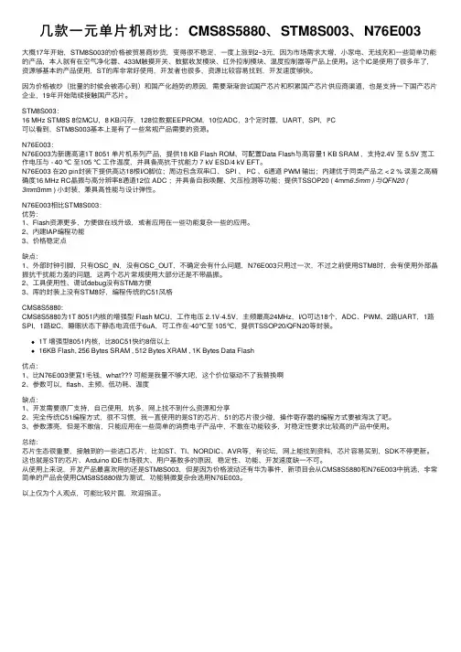
⼏款⼀元单⽚机对⽐:CMS8S5880、STM8S003、N76E003⼤概17年开始,STM8S003的价格被贸易商炒货,变得很不稳定,⼀度上涨到2~3元,因为市场需求⼤增,⼩家电、⽆线充和⼀些简单功能的产品,本⼈就有在空⽓净化器、433M触摸开关、数据收发模块、红外控制模块、温度控制器等产品上使⽤。
这个IC是使⽤了很多年了,资源够基本的产品使⽤,ST的库⾮常好使⽤,开发者也很多,资源⽐较容易找到,开发速度够快。
因为价格被炒(批量的时候会被恶⼼到)和国产化趋势的原因,需要渐渐尝试国产芯⽚和积累国产芯⽚供应商渠道,也是⽀持⼀下国产芯⽚企业,19年开始陆续接触国产芯⽚。
STM8S003:16 MHz STM8S 8位MCU,8 KB闪存,128位数据EEPROM,10位ADC,3个定时器,UART,SPI,I²C可以看到,STM8S003基本上是有了⼀些常规产品需要的资源。
N76E003:N76E003为新唐⾼速1T 8051 单⽚机系列产品,提供18 KB Flash ROM、可配置Data Flash与⾼容量1 KB SRAM ,⽀持2.4V ⾄ 5.5V 宽⼯作电压与 - 40 ℃⾄105 ℃⼯作温度,并具备⾼抗⼲扰能⼒ 7 kV ESD/4 kV EFT。
N76E003 在20 pin封装下提供⾼达18根I/O脚位;周边包含双串⼝、 SPI 、 I²C 、6通道 PWM 输出;内建优于同类产品之 < 2 % 误差之⾼精确度16 MHz RC晶振与⾼分辨率8通道12位 ADC ;并具备⾃我唤醒、⽋压检测等功能;提供TSSOP20 ( 4mm6.5mm ) 与QFN20 (3mm3mm ) ⼩封装,兼具⾼性能与设计弹性。
N76E003相⽐STM8S003:优势:1、Flash资源更多,⽅便做在线升级,或者应⽤在⼀些功能复杂⼀些的应⽤。
2、内建IAP编程功能3、价格稳定点缺点:1、外部时钟引脚,只有OSC_IN,没有OSC_OUT,不确定会有什么问题,N76E003只⽤过⼀次,不过之前使⽤STM8时,会有使⽤外部晶振抗⼲扰能⼒差的问题,这两个芯⽚常规使⽤⼤部分还是不带晶振。
STM8S开发环境搭建IAR For STM8标签:STM8SSTM8S-Discovery IAR2013-12-29 15:593139人阅读评论(0) 收藏举报分类:STM8S单片机(3)作者同类文章X版权声明:本文为博主原创文章,未经博主允许不得转载。
/*********************************************************************************************************************** ************* Name : STM8S开发环境搭建IAR For STM8* Author : MingMing* Release : 2013/12/29* Update : 2013/12/29* E-mail : clint.wang@********************************************************************************************************************** *************/本文采用的是STM8S-Discovery开发板,开发板上半部分为ST Link调试器,芯片采用的是STM32F103C8,下半部分是STM8S105C6的开发板。
对于STM8的开发环境,主要采用两种,一种是IAR For STM8,另一种是官方的ST Toolset。
ST Toolset中包含了两个工具STVD(ST Visual Develop)和STVP(ST Visual Programmer)。
STVD是一款开发工具,它自身并没集成编译器,因此需要安装第三方编译器Cosmic。
STVP 是一款烧录工具,它支持.hex .s19 .sx三种文件的烧录,对IAR编译出的.hex文件的烧录我们就不用太担心了。
stm8s 开发(一)使用IAR 新建工程
新建工程是第一步!
a)创建一个Workspace
首先,创建一个workspace。
选择菜单FileNewWorkspace
b)创建一个Project
1)创建一个新的工程,选择ProjectCreateNewProject,创建新工程的对话框,如下2)Toolchain默认是STM8Series。
无需再选择。
3)在Projecttemplates中选择“Emptyproject”
4)弹出SaveAs对话框,选择project保存的路径,并输入project的名字
5)在添加文件到工程中之前,先保存workspace。
选择FileSaveWorkspace,指定要保存的路径,并输入workspace的名字。
一个workspace文件的扩展名是eww.此文件列出了添加到workspace中的所有的project。
相关当前会话信息,比如windows的保存路径和断点保存于
projects\setttings目录下。
c)添加文件和组到工程
可选择ProjectAddFiles选择要添加的C文件。
找到相应的文件。
可选择ProjectAddGroup新建组。
d)工程选项配置
选择ProjectOptions,或者在Workspace窗口,选中project名字,右击选择选择“Options…”
1)在Category中,选择“GeneralOptions”,如2)在Category中,选择C/C++Compiler,显示compiler选项页
这里可以设置编译的优化,一般选择Low级别,若选用High级别的话,。
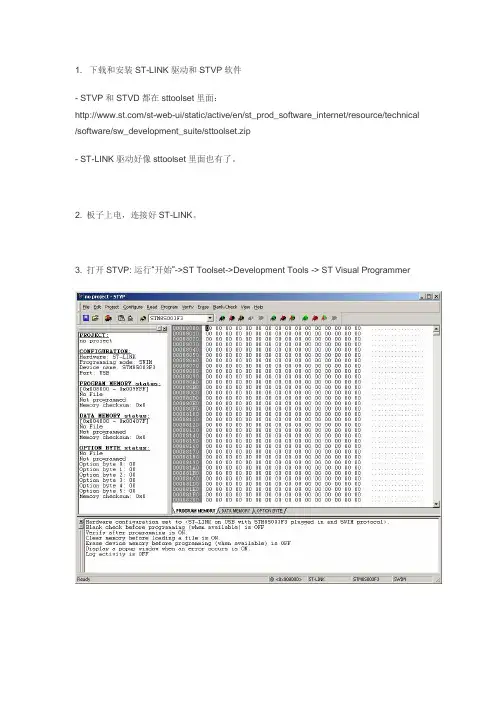
1. 下载和安装ST-LINK驱动和STVP软件- STVP和STVD都在sttoolset里面:/st-web-ui/static/active/en/st_prod_software_internet/resource/technical /software/sw_development_suite/sttoolset.zip- ST-LINK驱动好像sttoolset里面也有了。
2. 板子上电,连接好ST-LINK。
3. 打开STVP: 运行“开始”->ST Toolset->Development Tools -> ST Visual Programmer4. 连接配置:运行Configure -> Configure ST Visual Programmer 选择ST-LINK, USB, SWIM, STM8S003F35. 选择程序:运行File->Open,选择要下载的.hex或者.srec文件。
6. 下载程序:运行Program -> All tabs ,执行下载。
Hardware: 烧录工具。
Port: USB。
Programming mode: SWIM。
Device: 选择要烧录的型号。
打开要烧录的目标文件“File -> Open…”。
DATA MEMORY: EEPROM 数据区。
配置OPTION BYTE选项的界面如图2-67所示。
图2-67 配置OPTION BYTEValue: 可直接在此框内直接输入配置好的OPTION BYTE值,OPTION BYTE内容根据Value 的值自动配置好。
以STM8S105S4为例说明OPTION BYTE的配置。
如图2-68所示。
图2-68 OPTION BYTE配置举例ROP:读出保护设置。
若设置了ON,那么程序是就无法读出。
UBC [7:0]:用户启动代码区。
一般用户在做IAP时,需要保护的代码部分设置。
STM8S MCU family 8-bit microcontroller/mcuSeptember 2008STMicroelectronics’ STM8S family of general-purpose 8-bit Flash microcontrollers offers ideal solutions for industrial and appliance market requirements. An advanced core version combined with a 3-stage pipeline ranks the STM8S microcontroller in the top position for performance. The true embedded EEPROM and the calibrated RC oscillator bring a significant cost effectiveness to the majority of applications. An easy-to-use and intuitive development environment contributes to improving time to market.STM8S: robust and reliableIn addition to performance, comprehensive design specifications and specific peripheral features make the STM8S robust and reliable:n 2 internal RC oscillators with dual independent watchdogsn Clock security system (CSS) to monitor the failure of external clock source n Complementary copy of configuration option bytes and EMS reset n Low emission in accordance with the IEC 61967 standardsn Outstanding robustness performance according to IEC 1000-4-2 and IEC 1000-4-4 standards n High current injection immunity (1 µA leakage current when 4 mA current is injected in adjacent pin)n Dedicated firmware library compliant to Class B of IEC 60335STM8S20x Performance lineUp to 6 KB SRAM2nd UARTSTM8 core @ 24 MHzUARTLIN/Smartcard/IrDA I²C400 kHz multimasterSPI 10 MHz Up to 3 x 16-bit timer8-bit timer 2 x Watchdog (IWDG and WWDG)AWUBeeper 1/2/4 Khz 10-bit ADC Up to 16 channelXTAL16 MHz int.RC osc.128 MHz int.RC osc.SWIM Debug module STM8S10x Access lineSTM8 core @ 16 MHzCAN 2.0BUp to 2 KB SRAMSTM8 core @ 16 MHz Up to 2 KB EEPROMUp to 1 KB EEPROMUp to 128 KB FlashUp to 32 KB FlashSTM8S product linesSTM8 coren 1.6 CPI average n 20 MIPs peak @ 24 MHzn32-bit memory interface n 3-stage pipelinen 16-bit index registers n 20 addressing modesSTM8S MCU familySTM8S portfolioTSSOP20LQFP32LQFP44LQFP64LQFP80LQFP48(*) w/wo EEPROMPerformance linePin count Memory sizeVQFN20, VQFN32 and VQFN48 packages are under qualification Access line (*)Under development© STMicroelectronics - September 2008 - Printed in Italy - All rights reservedThe STMicroelectronics corporate logo is a registered trademark of the STMicroelectronics group of companies.All other names are the property of their respective owners.For more information on ST products and solutions,visit Order code: BRSTM8S0908Device summaryHardware and software development tools 1。
摘要在嵌入式应用中,微控制器作为逻辑控制和数值计算的核心,在软件和硬件的支持下完成产品功能。
产品硬件是通常不变的,它的更新频率非常低。
产品的软件操作产品硬件来完成逻辑功能,它可以通过软件更新来增强产品功能和修复功能缺陷,它的更新频率相对于硬件而言高的多。
软件升级常用的方式有在线编程方式(ICP)和在应用编程(IAP),在线编程需要单独将MCU 插入编程器,而在实际的嵌入式应用中,MCU已经嵌入产品硬件,单独拆除MCU是非常困难的,因此通常采用在在线编程的方式,经过MCU的外部通信接口进行软件升级。
本文针对汽车车身网络系统的研究,设计一种基于CAN总线的在线升级系统,实现对汽车各种电控单元(ECU)进行在线升级。
本文通过在STM8的ECU中实现了基于CAN总线通信的在线升级代码bootloader,通过IAP编程的字节编程实现对应用程序代码数据的更新。
在实现在线升级底层代码过程中,将升级代码bootloader存放在用户启动代码区域(UBC)中,防止意外的升级代码破坏,通过固定应用程序的中断向量表位置,并修改位于UBC空间的原始中断向量表的入口地址来解决更新后应用程序中断的使用。
通过对FLASH的IAP编程和中断向量的修改实现了STM8单片机的在线更新系统,本系统对STM8嵌入产品的软件升级提供了完整的支持。
【关键字】ECU 在线升级系统STM8 IAP CAN目录前言 (1)第一章在线升级简介 (2)第二章系统总体设计 (4)第一节软件总体设计 (4)第二节在线升级过程 (7)第三节下载协议 (10)第四节下载程序数据解析 (13)第三章基于STM8的在线升级系统 (15)第一节在线升级入口 (15)第二节升级流程控制 (16)第三节下载协议支持 (18)第四节FLASH编程接口 (19)第五节CAN通信 (21)第六节中断向量表搬移 (22)第四章系统实现及测试 (25)第一节编译器设置 (25)第二节Bootloader项目实现 (26)第三节应用程序测试项目 (33)第五节在线升级测试 (36)结论.................................................................................................................... 错误!未定义书签。
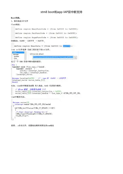
STM8 RAM我关于实现IAP 的理解,如果有误,希望可以得到大家的斧正1.IAP 部分程序和应用程序分开两个项目编写。
2.应用程序部分编译前要修改ICF 文件,使其代码安排到IAP 程序区外,如0x90003.IAP 项目编译前也要修改ICF 文件a.修改代码编译后所在ROM 中的位置,如:0x8000-0x8FFFb.按网友dianzidog给出的方法,实现ram 运行代码////////////////////////摘自网友dianzidog 的帖子/////////////////////////////////// icf 文件里面initialize by copy { ro section MyCodeInRAM };//这句是将代码在程序初始化的时候copy 到RAM 的。
place in NearData { ro section MyCodeInRAM };//定义段的位置c 文件里面void abc(void)@”MyCodeInRAM”//直接将函数限定在段中{ ...... ...... ...... }就完成iar 中ram 运行代码的步骤了//////////////////////////////////////////////////////////////////////////////////////////////4.IAP 程序经过IAR 编译后的HEX 文件,使用ST-LINK 将代码烧入CPU内5.应用程序则通过IAP 的上位机应用程序通过串口(假设使用UART1 协议)下载到已经有IAP 程序的CPU中去。
6.IAP 程序项目所需修改后的ICF 文件(暂时以STM8S103K 为修改对象,摘取与原文件不同部分):define region NearFuncCode = [from 0x8000 to 0x87FF];//假设BOOTLOADER 部分使用了2K 的代码空间define region FarFuncCode = [from 0x8000 to 0x87FF];define region HugeFuncCode = [from 0x8000 to 0x87FF];initialize by copy { ro section MyCodeInRAM };//这句是将代码在程序初始化的时候copy 到RAM 的。
实验题目:实验17—基于RFID的电子钱包应用实验实验时间:2016.1.4一、实验目的:了解RFID 相关知识。
掌握RFID 模块读写IC 卡数据的原理与方法。
二、实验原理及程序分析:1、STM8S处理器概述本实验所使用RFID 模块由STM8处理器和MFRC531(高集成非接触读写芯片)两片芯片搭建而成的。
STM8是基于8 位框架结构的微控制器,其CPU 内核有6 个内部寄存器,通过这些寄存器可高效地进行数据处理。
STM8的指令集支持80条基本语句及20种寻址模式,而且CPU的6 个内部寄存器都拥有可寻址的地址。
ST M8 内部的FLASH程序存储器和数据EEPROM由一组通用寄存器来控制。
用户可以使用这些寄存器来编程或擦除存储器的内容、设置写保护、或者配置特定的低功耗模式。
用户也可以对器件的选项字节(Option byte) 进行编程。
FLASH●STM8S EEPROM 分为两个存储器阵列:─最多至128K字节的FLASH程序存储器,不同的器件容量有所不同。
─最多至2K字节的数据EEPROM(包括option byte -选择字节),不同的器件容量有所不同。
●编程模式─字节编程和自动快速字节编程(没有擦除操作)─字编程─块编程和快速块编程(没有擦除操作)─在编程/ 擦除操作结束时和发生非法编程操作时产生中断●读同时写(RWW)功能。
该特性并不是所有STM8S器件都拥有。
●在应用编程(IAP)和在线编程(ICP)能力。
●保护特性─存储器读保护(ROP)─基于存储器存取安全系统(MASS 密钥)的程序存储器写保护─基于存储器存取安全系统(MASS 密钥)的数据存储器写保护─可编程的用户启动代码区域(UBC) 写保护●在待机(Halt) 模式和活跃待机(Active-halt)模式下,存储器可配置为运行状态和掉电状态。
数据EEPROM(DATA) 区域可用于存储用户具体项目所需的数据。
默认情况下,DATA 区域是写保护的,这样可以在主程序工作在IAP 模式时防止DATA 区域被无意地修改。
STM8 ICP 和IAP在线编程(ICP)用于更新STM8 整个存储器的内容。
ICP 使用SWIM 接口把用户的程序装载到微控制器中,同时提供迅速而有效的设计迭代并且去除了不必要的封装处理和器件插槽。
SWIM 接口(单线接口模块)使用SWIM 引脚和编程工具相连接。
相对于ICP 方式,在应用编程(IAP)可使用STM8 支持的任意通讯接口(I/O、I2C、SPI、UART)来下载要编入存储器中的数据。
IAP 允许在应用程序运行中对FLASH 程序存储器的内容重新编程。
然而要想使用IAP,必须通过ICP 对FLASH 程序存储器预先编程。
请参考STM8 Flash 编程手册(PM0051)和STM8 SWIM 通信协议和调试模块用户手册(UM0470)来了解关于编程步骤的更多细节。
R/W/E=读;写和运行;R/E=读和运行(写操作被禁止);R=读(写操作和运行被禁止);P=该区域不可存取(读;写和运行被禁止);P/WROP=被保护。
除ROP 选项字节外,写操作被禁止。
在向FLASH_PUKR 写入正确的MASS 密钥之前,Flash 程序存储器是写保护的(锁住)。
可以通过清PUL 位来重新锁住该区域,但在两次复位之间仅可解锁一次。
在向FLASH_DUKR 写入正确的MASS 密钥之前,DATA 存储器是写保护的(锁住)。
可以通过清DUL 位来重新锁住该区域。
如果想对UBC 区域编程,首先要清除UBC 对应的选项字节位。
在向FLASH_DUKR 写入正确的MASS 密钥(同时OPT 位要置1)之前,选项字节是写保护的(锁住)。
可以通过清DUL 位来重新锁住该区域。
当ROP 位被清除,整个存储器(包括选项字节)被自动擦除。
tips:感谢大家的阅读,本文由我司收集整编。
仅供参阅!。
不知是心血来潮,还是其它因素,突然又想起玩汇编语言了。
这几年也没少跟单片机打交道,包括51系列,430系列,ARM系列,但都是用C语言来开发。
不过由于使用C语言,实际上对这些CPU的了解还是不够深刻,当然除了51之外,因为那是我多年前曾经用汇编开发过的芯片。
尽管当今C语言已经在嵌入式产品的开发过程中成为主流,但我个人依然认为,要想真正了解CPU的特点,还得用汇编语言。
不知道这种观点是对还是错,也许是因为自己从硬件做起,写过机器码,用汇编语言做过优化,因此对汇编语音有一种特殊的偏爱。
51系列的芯片用多了,感觉有时写起程序来不太方便,因此总想寻找一些其它的8位单片机玩玩,正好手头有一个ST的三合一开发板,那是09年参加ST研讨会上买的,一直躺在那里,与其躺在那里,不如拿出来玩玩。
这几年,ST在国内推广STM32,力度不小,不过我一直没有用过,只是初步地看看资料。
原因在于在32位单片机方面,我一直在用Luminary公司的LM3S1138,感觉不错,一直都很顺利。
09年ST举办的研讨会上,ST除了介绍STM32外,也介绍了STM8,当时听了以后,觉得还行。
尤其是会上的低功耗演示给我留下了很深刻的印象。
基于这些,我决定好好地玩一下STM8芯片,并将玩的结果拿出来与大家共享。
STM8与汇编语言(2)第一次打开STM8的手册时发现,CPU中的寄存器只有6个,即A、X、Y、SP、PC 和CC。
这几个寄存器,看上去特象早年苹果机使用的微处理器6502。
在眼下都是多寄存器的RISC潮流下,不知ST推出的这种CPU架构有什么意图?这样的芯片能否与Microchip 或者Atmel的RISC结构的MCU竞争呢?在此我无意做评论,我只想了解这颗芯片。
通过仔细研究,我发现由于STM8采用了32位宽度的程序存储器结构,使得大部分的指令都能在一个周期内取出,并且采用了哈佛结构和流水线,相当多的指令也都是单周期完成的。
这样的话,虽然CPU是CISC架构的,但也基本上达到了单周期指令的效果,就像手册上说的,CPU的性能达到了20MISP◎24MHZ。
STM8集成开发环境STVD建立目的:将按模块划分放在D:\Project\SV6400\Source\Source\SV64E0\source下的文件编译连接之后形成调试和烧录的文件。
文件结构为下图:其中lib文件上放了STM8的库文件。
IAP放了旧版本CXSTM8V4.2.2编译之后的IAP.o和stm8_flash.o.这样在新版本下能兼容旧版本下的升级功能。
Config文件夹下放了链接配置文件SV64E0_M8.lkf。
其他文件夹下面包含相应的.c,.h或.s文件。
一.建立工作空间(Workspace)。
工作空间是管理项目和它的各项目的源代码,一个工作空间可以包含多个项目。
1.1.In the main menu bar select File>New Workspace.2.In the New Workspace window, click on the Create Empty Workspaceicon and then OK.3.Enter a name in the Workspace Filename field. 如STM8_Workspace4.Enter the pathname where you want to store the workspace in theWorkspace Location field, 如D:\Project\STM8_Workspace .then click on OK.5.Save your workspace, select File>Save Workspace产生效果:1.STVD'的工作空间窗口下出现STM8_Workspace.stw的图标。
2.工作空间目录D:\Project\STM8_Workspace下包含STM8_Workspace.stw和STM8_Workspace.wed3.此时工作空间下还没有具体项目,因此不能进行编译等操作。
STM8S做IAP
一:环境与平台
MCU:STM8S005K6
集成开发环境:STVD
开发方式:库开发
芯片内部存储”偷窥”软件Smart PRO 2008
二:在RAM中运行代码
0.在STM8s.h中将#define RAM_EXECUTION (1)的注释去掉,以使用RAM功能.
1. 利用编译器函数#pragma section (FLASH_CODE) , #pragma section () 对函数void FLASH_ProgramBlock(Num,PROG, FAST ,Buffer);进行声明.FLASH_CODE是声明的这段代码的名字,可以自己随便取.
同时函数用IN_RAM包括.
举例代码如下:
#pragma section (FLASH_CODE)
IN_RAM(void FLASH_ProgramBlock(Num,PROG, FAST ,Buffer))
{
Num=PROG+ FAST +Buffer;
}
#pragma section ()
2.声明编译器函数int _fctcpy(char name);
3.在函数FLASH_ProgramBlock运行前时,利用编译器函数int _fctcpy(char name)将函数FLASH_ProgramBlock复制到RAM中.形参char name是指要复制的代码段名字的首字母.此例中要复制的代码段名为FLASH_CODE.所以应该写成: _fctcpy('F');
4.在STVD软件, project工程, seting设置, linker链接器, Gategory , Input , RAM 栏中添加要在RAM中运行的代码" . FLASH_CODE"名, 并在option中输入"-ic".具体见图片.
如果出现没有" . FLASH_CODE"的默认位置这样的错误,说明这步没有处理好.
三:STM8S的中断特性
1 把APP的中断向量表地址改成0xa300 , Flash地址改成oxa380 , 之后程序不能执行.
把APP的中断向量表地址改成0x8000 , Flash地址改成oxa380 , 之后程序就能执行.是因为一上电STM8S就读取0x8000-0x8003的复位地址,以实现复位,但找不到. 这异常与复位中断有关,STM8S读取中断向量表的地址只能是0x8000到0x8080.谁的复位函数地址处在0x8000,就复谁的位.复位就是跳转主函数开始地址的意思.STM8S单片机主函数地址/复位地址是0x8000-0x8003.
地址0x8004-0x8080为其它中断函数地址
2.局部的变量,全局的变量,都在主函数运行后被赋初值或运行中改变值,这些变量都存储在RAM中.只有code/const指定了的才会在ROM中.
3.可以利用软件复位实现软件间跳转(跳转前修改地址0x8000-0x8003中复位函数的地址); 也可直接利用跳转指令实现跳转.
四:操作流程
1 :APP软件,在STVD软件中,工程->设置->Linker->Caneral->Input中,设置中断地址0xa300 , Flash地址0xa380 .设置是否完成会在.lkf文件中看到,这是地址分配文件
2 :Boot软件,在软件中利用汇编指令跳转到APP代码Flash的开始地址.
_asm("LDW X, SP ");
_asm("LD A, $FF");
_asm("LD XL, A ");
_asm("LDW SP, X ");
_asm("JPF $A380"); //跳转到APP Flash地址0xA380
嵌入app.bin的地址为偏移地址,包含中断向量表地址/Flash 地址.
Boot代码的地址分配默认.
3.利用smart Pro软件将APP.hex文件转化成APP.bin
4.利用二进制软件,修剪无用数据
5.先在smart pro 2008中导入Boot.hex ,再导入修剪过的app.bin , 最后保存为Down.hex即可. 注意,导入app.bin时,不要清除之前导入的Boot代码.同时注意导入的app.bin 文件的Flash地址,导入到缓冲区的地址(器件地址)要对应跳转地址.
五:Smart PRO 2008的应用.
1.该软件可作一般二进制处理软件使用.但其特别之处在于,它的显示区/缓冲区/器件存储区都是基于具体真实的芯片存储架构,所以比一般的二进制软件好操作芯片的存储.具体操作在此不说明,可单独联系我.
六:声明/其它
1:以上内容为个人观点,没有经过严格测试,如有使用,请使用者自行评估风险,出现问题本人一概不负责!
2:技术交流:3228504429。