1
640120f
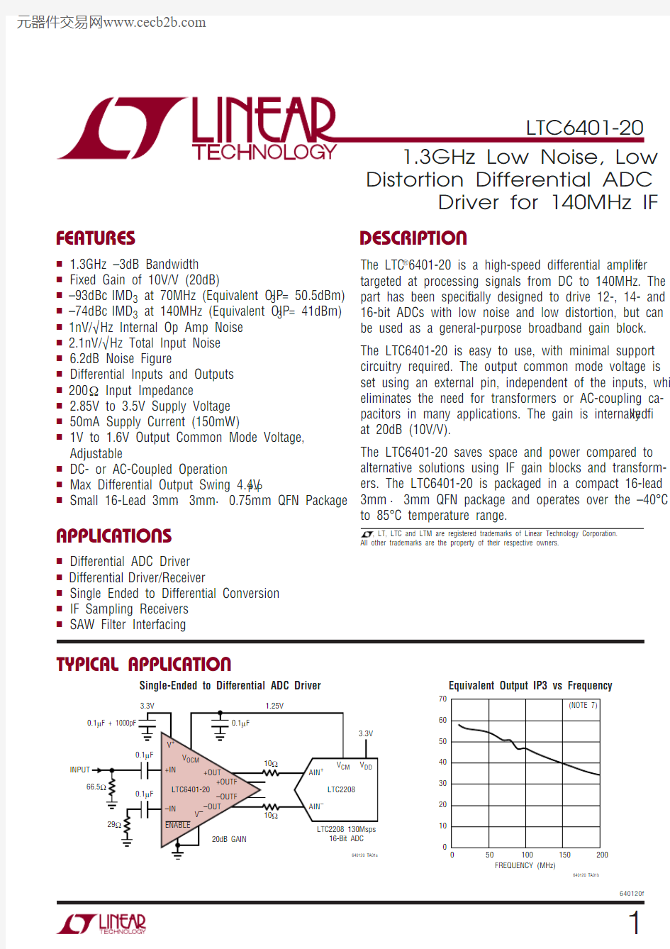
TYPICAL APPLICATION
FEATURES
APPLICATIONS
DESCRIPTION
Distortion Differential ADC
Driver for 140MHz IF
The LTC ?6401-20 is a high-speed differential ampli? er targeted at processing signals from DC to 140MHz. The part has been speci? cally designed to drive 12-, 14- and 16-bit ADCs with low noise and low distortion, but can also be used as a general-purpose broadband gain block.The LTC6401-20 is easy to use, with minimal support circuitry required. The output common mode voltage is set using an external pin, independent of the inputs, which eliminates the need for transformers or AC-coupling ca-pacitors in many applications. The gain is internally ? xed at 20dB (10V/V).
The LTC6401-20 saves space and power compared to alternative solutions using IF gain blocks and transform-ers. The LTC6401-20 is packaged in a compact 16-lead 3mm × 3mm QFN package and operates over the –40°C to 85°C temperature range.
■
1.3GHz –3dB Bandwidth ■ Fixed Gain of 10V/V (20dB)■ –93dBc IMD 3 at 70MHz (Equivalent OIP 3 = 50.5dBm)■ –74dBc IMD 3 at 140MHz (Equivalent OIP 3 = 41dBm)■ 1nV/√H z Internal Op Amp Noise ■
2.1nV/√H z Total Input Noise ■ 6.2dB Noise Figure
■ Differential Inputs and Outputs ■ 200Ω Input Impedance
■ 2.85V to 3.5V Supply Voltage ■ 50mA Supply Current (150mW)
■ 1V to 1.6V Output Common Mode Voltage, Adjustable
■ DC- or AC-Coupled Operation
■
Max Differential Output Swing 4.4V P-P
■ Small 16-Lead 3mm × 3mm × 0.75mm QFN Package
■
Differential ADC Driver ■ Differential Driver/Receiver
■ Single Ended to Differential Conversion ■ IF Sampling Receivers ■ SAW Filter Interfacing
Single-Ended to Differential ADC Driver
Equivalent Output IP3 vs Frequency
FREQUENCY (MHz)
0O U T P U T I P 3 (d B m )
70(NOTE 7)
60
50403020100
10050
150
640120 TA01b
200
LTC6401-20
2
640120f
ABSOLUTE MAXIMUM RATINGS
Supply Voltage (V + – V –) ..........................................3.6V Input Current (Note 2) ..........................................±10mA Operating Temperature Range
(Note 3) ...............................................–40°C to 85°C Speci? ed Temperature Range
(Note 4) ...............................................–40°C to 85°C Storage Temperature Range ...................–65°C to 150°C Maximum Junction Temperature...........................150°C
(Note 1)
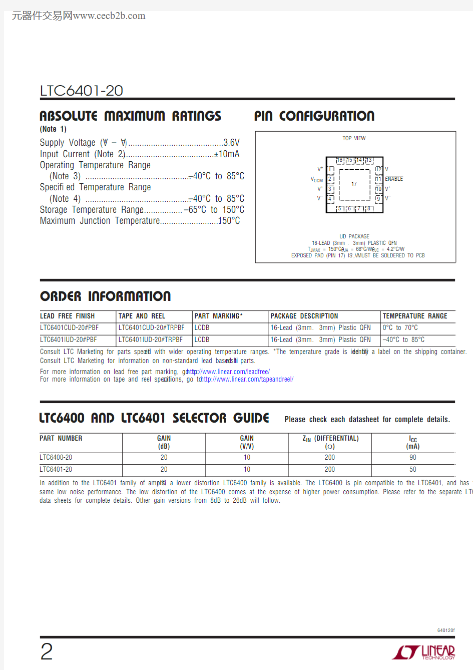
16151413
5678TOP VIEW UD PACKAGE
16-LEAD (3mm × 3mm) PLASTIC QFN 9101117
124
321V +V OCM V +V –V –
ENABLE V +V ––I N
–I N
+I N +I N
–O U T
–O U T F
+O U T F
+O U T
T JMAX = 150°C, θJA = 68°C/W, θJC = 4.2°C/W
EXPOSED PAD (PIN 17) IS V –, MUST BE SOLDERED TO PCB
ORDER INFORMATION
LTC6400 AND LTC6401 SELECTOR GUIDE
PART NUMBER GAIN
(dB)GAIN (V/V)Z IN (DIFFERENTIAL)
(Ω)
I CC (mA)LTC6400-20201020090LTC6401-20
20
10
200
50
In addition to the LTC6401 family of ampli? ers, a lower distortion LTC6400 family is available. The LTC6400 is pin compatible to the LTC6401, and has the same low noise performance. The low distortion of the LTC6400 comes at the expense of higher power consumption. Please refer to the separate LTC6400 data sheets for complete details. Other gain versions from 8dB to 26dB will follow.
Please check each datasheet for complete details.
PIN CONFIGURATION
LEAD FREE FINISH TAPE AND REEL PART MARKING*PACKAGE DESCRIPTION
TEMPERATURE RANGE LTC6401CUD-20#PBF LTC6401CUD-20#TRPBF LCDB 16-Lead (3mm × 3mm) Plastic QFN 0°C to 70°C LTC6401IUD-20#PBF
LTC6401IUD-20#TRPBF
LCDB
16-Lead (3mm × 3mm) Plastic QFN
–40°C to 85°C
Consult LTC Marketing for parts speci? ed with wider operating temperature ranges. *The temperature grade is identi? ed by a label on the shipping container.Consult LTC Marketing for information on non-standard lead based ? nish parts.For more information on lead free part marking, go to: https://www.doczj.com/doc/751753759.html,/leadfree/ For more information on tape and reel speci? cations, go to: https://www.doczj.com/doc/751753759.html,/tapeandreel/
LTC6401-20
3
640120f
DC ELECTRICAL CHARACTERISTICS SYMBOL PARAMETER CONDITIONS
MIN TYP MAX UNITS Input/Output Characteristic
G DIFF Gain
V IN = ±100mV Differential ●19.4
2020.6dB G TEMP Gain Temperature Drift V IN = ±100mV Differential
●1mdB/°C
V SWINGMIN Output Swing Low Each Output, V IN = ±400mV Differential ●90
170
mV V SWINGMAX Output Swing High
Each Output, V IN = ±400mV Differential ●
2.3 2.44V V OUTDIFFMAX Maximum Differential Output Swing 1dB Compressed 4.4
V P-P I OUT Output Current Drive Single-Ended ●10mA
V OS Input Offset Voltage Differential ●–2
2
mV TCV OS Input Offset Voltage Drift
Differential
● 1.4
μV/°C
I VRMIN Input Common Mode Voltage Range, MIN 1
V I VRMAX Input Common Mode Voltage Range, MAX 1.6
V R INDIFF Input Resistance Differential
●
170200230ΩC INDIFF Input Capacitance Differential, Includes Parasitic 1pF R OUTDIFF Output Resistance Differential ●182532ΩR OUTFDIFF Filtered Output Resistance Differential
●85100115
ΩC OUTFDIFF Filtered Output Capacitance Differential, Includes Parasitic
2.7pF CMRR Common Mode Rejection Ratio Input Common Mode Voltage 1.1V to 1.4V ●45
66dB Output Common Mode Voltage Control
G CM Common Mode Gain
V OCM = 1V to 1.6V
1
V/V
V OCMMIN Output Common Mode Range, MIN
●
11.1
V V V OCMMAX Output Common Mode Range, MAX
●
1.61.5V V V OSCM Common Mode Offset Voltage V OCM = 1.1V to 1.5V
●–15
15
mV TCV OSCM Common Mode Offset Voltage Drift ●6μV/°C IV OCM V OCM Input Current ●
5
15μA E N A B L E Pin V IL E N A B L E Input Low Voltage ●0.8
V V IH E N A B L E Input High Voltage ●
2.4
V I IL E N A B L E Input Low Current E N A B L E = 0.8V ●±0.5
μA I IH
E N A B L E Input High Current E N A B L E = 2.4V
●
1.2
3μA Power Supply V S Operating Supply Range ●
2.853
3.5V I S Supply Current
E N A B L E = 0.8V ●385062mA I SHDN Shutdown Supply Current E N A B L E = 2.4V ●13mA PSRR
Power Supply Rejection Ratio (Differential Outputs)
2.85V to
3.5V
●
55
84
dB
The ● denotes the speci? cations which apply over the full operating
temperature range, otherwise speci? cations are at T A = 25°C. V + = 3V, V –
= 0V, +IN = –IN = V OCM = 1.25V, E N A B L E = 0V, No R L unless
otherwise noted.
LTC6401-20
4
640120f
AC ELECTRICAL CHARACTERISTICS
Speci? cations are at T A = 25°C. V + = 3V, V – = 0V, +IN and –IN
? oating, V OCM = 1.25V, E N A B L E = 0V, No R L unless otherwise noted.
SYMBOL PARAMETER CONDITIONS MIN
TYP MAX
UNITS –3dBBW –3dB Bandwidth
200mV P-P ,OUT (Note 6) 1.25GHz 0.1dBBW Bandwidth for 0.1dB Flatness 200mV P-P ,OUT (Note 6)130MHz 0.5dBBW Bandwidth for 0.5dB Flatness 200mV P-P ,OUT (Note 6)
250MHz 1/f 1/f Noise Corner 12.5kHz SR Slew Rate Differential (Note 6)4500V/μs t S1%1% Settling Time
2V P-P ,OUT (Note 6)2ns t OVDR Output Overdrive Recovery Time 1.9V P-P ,OUT (Note 6)
7ns t ON Turn-On Time +OUT, –OUT Within 10% of Final Values 78ns t OFF Turn-Off Time
I CC Falls to 10% of Nominal
146ns –3dBBW CM
Common Mode Small Signal –3dB BW
0.1V P-P at V OCM , Measured Single-Ended at Output (Note 6)
15
MHz
10MHz Input Signal HD 2,10M /HD 3,10M
Second/Third Order Harmonic
Distortion
2V P-P ,OUT , R L = 400Ω–122/–92dBc 2V P-P ,OUT , No R L –110/–103dBc 2V P-P ,OUTFILT , No R L
–113/–102dBc IMD 3,10M
Third-Order Intermodulation (f1 = 9.5MHz f2 = 10.5MHz)
2V P-P ,OUT Composite, R L = 400Ω–96dBc 2V P-P ,OUT Composite, No R L –108dBc 2V P-P ,OUTFILT Composite, No R L
–105dBc OIP 3,10M Third-Order Output Intercept Point (f1 = 9.5MHz f2 = 10.5MHz)2V P-P ,OUT Composite, No R L (Note 7)58dBm P 1dB,10M 1dB Compression Point R L = 375Ω (Notes 5, 7)17.3dBm NF 10M Noise Figure
R L = 375Ω (Note 5)
6.2dB e IN,10M Input Referred Voltage Noise Density
Includes Resistors (Short Inputs)
2.1nV/√H z e ON,10M
Output Referred Voltage Noise Density Includes Resistors (Short Inputs)
21
nV/√H z
70MHz Input Signal HD 2,70M /HD 3,70M
Second/Third Order Harmonic Distortion
2V P-P ,OUT , R L = 400Ω–91/–80dBc 2V P-P ,OUT , No R L –95/–88dBc 2V P-P ,OUTFILT , No R L
–95/–88dBc IMD 3,70M
Third-Order Intermodulation (f1 = 69.5MHz f2 = 70.5MHz)
2V P-P ,OUT Composite, R L = 400Ω–88dBc 2V P-P ,OUT Composite, No R L –93dBc 2V P-P ,OUTFILT Composite, No R L
–92dBc OIP 3,70M Third-Order Output Intercept Point (f1 = 69.5MHz f2 = 70.5MHz)2V P-P ,OUT Composite, No R L (Note 7)50.5dBm P 1dB,70M 1dB Compression Point R L = 375Ω (Notes 5, 7)17.3dBm NF 70M Noise Figure
R L = 375Ω (Note 5)
6.1dB e IN,70M Input Referred Voltage Noise Density
Includes Resistors (Short Inputs)
2.1nV/√H z e ON,70M
Output Referred Voltage Noise Density Includes Resistors (Short Inputs)
21
nV/√H z
140MHz Input Signal
HD 2,140M /HD 3,140M Second/Third Order Harmonic
Distortion
2V P-P ,OUT , R L = 400Ω–80/–57dBc 2V P-P ,OUT , No R L –81/–60dBc 2V P-P ,OUTFILT , No R L
–80/–65
dBc
LTC6401-20
5
640120f
AC ELECTRICAL CHARACTERISTICS FREQUENCY (MHz)
P H A S E (D E G R E E )
100
0–100–200–300
–400
GROUP DELAY (ns)
1.5
1.2
0.9
0.6
0.3
0200
400600800
1000
640120 G03
FREQUENCY (MHz)
10
100
1000
N O R M A L I Z E D G A I N (d B )
1.00.8
–0.8
0.6
–0.60.4–0.40.2–0.20
–1.0
640120 G02
FREQUENCY (MHz)
10
1001000
3000
G A I N (d B )
25
20
15105
0640120 G01
Note 1: Stresses beyond those listed under Absolute Maximum Ratings may cause permanent damage to the device. Exposure to any Absolute Maximum Rating condition for extended periods may affect device reliability and lifetime.
Note 2: Input pins (+IN, –IN) are protected by steering diodes to either supply. If the inputs go beyond either supply rail, the input current should be limited to less than 10mA.
Note 3: The LTC6401C and LTC6401I are guaranteed functional over the operating temperature range of –40°C to 85°C.Note 4: The LTC6401C is guaranteed to meet speci? ed performance from 0°C to 70°C. It is designed, characterized and expected to meet speci? ed performance from –40°C to 85°C but is not tested or QA sampled at these
temperatures. The LTC6401I is guaranteed to meet speci? ed performance from –40°C to 85°C.
Note 5: Input and output baluns used. See Test Circuit A.Note 6: Measured using Test Circuit B.
Note 7: Since the LTC6401-20 is a feedback ampli? er with low output impedance, a resistive load is not required when driving an AD converter. Therefore, typical output power is very small. In order to compare the LTC6401-20 with ampli? ers that require 50Ω output load, the LTC6401-20 output voltage swing driving a given R L is converted to OIP 3 and P 1dB as if it were driving a 50Ω load. Using this modi? ed convention, 2V P-P is by de? nition equal to 10dBm, regardless of the actual R L .
TYPICAL PERFORMANCE CHARACTERISTICS
Frequency Response
Gain 0.1dB Flatness
S21 Phase and Group Delay vs Frequency
SYMBOL PARAMETER
CONDITIONS
MIN
TYP MAX
UNITS IMD 3,140M
Third-Order Intermodulation
(f1 = 139.5MHz f2 = 140.5MHz)
2V P-P ,OUT Composite, R L = 400Ω–71dBc 2V P-P ,OUT Composite, No R L –74dBc 2V P-P ,OUTFILT Composite, No R L –72dBc OIP 3,140M Third-Order Output Intercept Point
(f1 = 139.5MHz f2 = 140.5MHz)2V P-P ,OUT Composite, No R L (Note 7)41dBm P 1dB,140M 1dB Compression Point R L = 375Ω (Notes 5, 7)18dBm NF 140M Noise Figure
R L = 375Ω (Note 5)
6.4dB e IN,140M Input Referred Voltage Noise Density
Includes Resistors (Short Inputs)
2.1nV/√H z e ON,140M Output Referred Voltage Noise Density Includes Resistors (Short Inputs)22nV/√H z IMD 3,130M/150M
Third-Order Intermodulation (f1 = 130MHz f2 = 150MHz) Measure at 170MHz
2V P-P ,OUT Composite, R L = 375Ω (Note 5)–61–69
dBc
Speci? cations are at T A = 25°C. V + = 3V, V – = 0V, +IN and –IN
? oating, V OCM = 1.25V, E N A B L E = 0V, No R L unless otherwise noted.
LTC6401-20
6
640120f
TIME (ns)
O U T P U T V O L T A G E (V )
2.5
0.5
1.0
2.01.5
050
100150
200
640120 G10
TIME (ns)
S E T T L I N G (%)
5432
1–4–3–2
–1–501
2
35
4
6
640120 G11
05
101520
TIME (ns)
O U T P U T V O L T A G E (V )
2.5
0.5
1.0
2.0
1.5
640120 G09
TIME (ns)
0O U T P U T V O L T A G E (V )
1.35
1.20
1.25
1.30
1.15
5
101520
640120 G08
FREQUENCY (MHz)
10
N O I S E F I G U R E (d B )
1510241214680
113513791INPUT REFERRED NOISE VOLTAGE (nV/√Hz)
6
4
2
0100
1000
640120 G07
FREQUENCY (MHz)
1
I M P E D A N C E M A G N I T U D E (Ω)
2502001501005002251751257525IMPEDANCE PHASE (DEGREE)
10080604020–80–60–40–200–100101001000
640120 G05
FREQUENCY (MHz)
10
S P A R A M E T E R S (d B )
0–10
–20–30–40–50–60–70–80
10010003000
640120 G04
TYPICAL PERFORMANCE CHARACTERISTICS
Input and Output Re? ection and Reverse Isolation vs Frequency
Input and Output Impedance vs Frequency
PSRR and CMRR vs Frequency
Overdrive Transient Response
1% Settling Time for 2V Output Step
Noise Figure and Input Referred Noise Voltage vs Frequency
Small Signal Transient Response
Large Signal Transient Response
FREQUENCY (MHz)
1
P S R R , C M R R (d B )
1009080706050403001020101001000
640120 G06
LTC6401-20
7
640120f
OUTPUT COMMON MODE VOLTAGE (V)
1.0
1.1 1.2 1.3 1.4
1.5640120 G18
D I S T O R T I O N (d B c )
–40
–50–60
–80–90–70–100
FREQUENCY (MHz)
T H I R D O R D E R I M D (d B c )
640120 G17
50
100
150
200
–40–50–60–80–90–70–120
–110–100–40
–50–60–80–90–70–120
–110–1000
50
100150
200
FREQUENCY (MHz)
H A R M O N I C
D I S T O R T I O N (d B c )
640120 G16
50
100150
200
–40–50–60–80–90–70–120
–110–100FREQUENCY (MHz)
H A R M O N I C D I S T O R T I O N (d B c )
640120 G15
640120 G13
FREQUENCY (MHz)
H A R M O N I C D I S T O R T I O N (d B c )
–40
–50–60–80–90–70–120
–110–1000
50
100150
200
50
100150
200
–40–50–60–80–90–70–120
–110–100FREQUENCY (MHz)
T H I R D O R D E R I M D (d B c )
640120 G14
FREQUENCY (MHz)
H A R M O N I C D I S T O R T I O N (d B c )
640120 G12
50
100150
200
–40–50–60–80–90–70–120
–110–100TYPICAL PERFORMANCE CHARACTERISTICS
Harmonic Distortion (Un? ltered) vs Frequency
Harmonic Distortion (Filtered) vs Frequency
Third Order Intermodulation Distortion vs Frequency
Harmonic Distortion (Un? ltered) vs Frequency
Harmonic Distortion (Filtered) vs Frequency
Third Order Intermodulation Distortion vs Frequency
Harmonic Distortion vs Output
Common Mode Voltage (Un? ltered Outputs)
Equivalent Output 1dB
Compression Point vs Frequency
FREQUENCY (MHz)
50O U T P U T 1d B C O M P R E S S I O N (d B m )
20
19
18
16
17
15
80
110140170200
640020 G19
LTC6401-20
8
640120f
TIME (ns)
–100
0V O L T A G E (V )
3.52.02.51.01.53.0–0.50.5
100
200300400
500
640120 G22
SUPPLY CURRENT (mA)
7040
60–1020305010
TIME (ns)
–100
V O L T A G E (V )
3.52.02.51.01.53.0–0.50.5
0100
200300400
500
640120 G21SUPPLY CURRENT (mA)
704060–1020305010
50
100150
200
FREQUENCY (MHz)
640120 G20
O U T P U T I P 3 (d B m )
706050
402010300
TYPICAL PERFORMANCE CHARACTERISTICS
Equivalent Output Third Order Intercept vs Frequency
Turn-On Time
Turn-Off Time
LTC6401-20
9
640120f
BLOCK DIAGRAM
PIN FUNCTIONS
V + (Pins 1, 3, 10): Positive Power Supply (Normally tied to 3V or 3.3V). All three pins must be tied to the same voltage. Bypass each pin with 1000pF and 0.1μF capaci-tors as close to the pins as possible.
V OCM (Pin 2): This pin sets the output common mode voltage. A 0.1μF external bypass capacitor is recom-mended.
V – (Pins 4, 9, 12, 17): Negative Power Supply. All four pins must be connected to the same voltage/ground.–OUT, +OUT (Pins 5, 8): Un? ltered Outputs. These pins have 12.5Ω series resistors.
–OUTF, +OUTF (Pins 6, 7): F iltered Outputs. These pins have 50Ω series resistors and a 1.7pF shunt capacitance.E N A B L E (Pin 11): This pin is a logic input referenced to V –. If low, the part is enabled. If high, the part is disabled and draws approximately 1mA supply current. +IN (Pins 13, 14): Positive Input. Pins 13 and 14 are internally shorted together.
–IN (Pins 15, 16): Negative Input. Pins 15 and 16 are internally shorted together.
Exposed Pad (Pin 17): V –. The Exposed Pad must be con-nected to the same voltage/ground as pins 4, 9, 12.
ENABLE
LTC6401-20
10
640120f
APPLICATIONS INFORMATION
Circuit Operation
The LTC6401-20 is a low noise and low distortion fully differential op amp/ADC driver with:
? Operation from DC to 1.3GHz –3dB bandwidth impedance ? Fixed gain of 10V/V (20dB) ? Differential input impedance 200Ω ? Differential output impedance 25Ω ? Differential impedance of output ? lter 100ΩThe LTC6401-20 is composed of a fully differential ampli? er with on chip feedback and output common mode voltage control circuitry. Differential gain and input impedance are set by 100Ω/1000Ω resistors in the feedback network. Small output resistors of 12.5Ω improve the circuit stability over various load conditions. They also provide a possible external ? ltering option, which is often desirable when the load is an ADC.
Filter resistors of 50Ω are available for additional ? ltering. Lowpass/bandpass ? lters are easily implemented with just a couple of external components. Moreover, they offer single-ended 50Ω matching in wideband applications and no external resistor is needed.
The LTC6401-20 is very ? exible in terms of I/O coupling. It can be AC- or DC-coupled at the inputs, the outputs or both. Due to the internal connection between input and output, users are advised to keep input common mode voltage between 1V and 1.6V for proper operation. If the inputs are AC-coupled, the input common mode voltage is automatically biased close to V OCM and thus no external circuitry is needed for bias. The LTC6401-20 provides an output common mode voltage set by V OCM , which allows driving an ADC directly without external components such as a transformer or AC coupling capacitors. The input signal can be either single-ended or differential with only minor differences in distortion performance.Input Impedance and Matching
The differential input impedance of the LTC6401-20 is 200Ω. If a 200Ω source impedance is unavailable, then
the differential inputs may need to be terminated to a lower value impedance, e.g. 50Ω, in order to provide an imped-ance match to the source. Several choices are available. One approach is to use a differential shunt resistor (Figure 1). Another approach is to employ a wideband transformer (Figure 2). Both methods provide a wideband match. The termination resistor or the transformer must be placed close to the input pins in order to minimize the re? ection due to input mismatch. Alternatively, one could apply a narrowband impedance match at the inputs of the LTC6401-20 for frequency selection and/or noise reduction.Referring to F igure 3, LTC6401-20 can be easily con? gured for single-ended input and differential output without a balun. The signal is fed to one of the inputs through a matching network while the other input is connected to the same matching network and a source resistor. Because the return ratios of the two feedback paths are equal, the
Figure 1. Input Termination for Differential 50Ω Input Impedance Using Shunt Resistor
Figure 2. Input Termination for Differential 50Ω Input Impedance Using a 1:4 Balun
LTC6401-20
11
640120f
two outputs have the same gain and thus symmetrical swing. In general, the single-ended input impedance and termination resistor R T are determined by the combination of R S , R G and R F . For example, when R S is 50Ω, it is found that the single-ended input impedance is 200Ω and R T is 66.5Ω in order to match to a 50Ω source impedance.The LTC6401-20 is unconditionally stable. However, the overall differential gain is affected by both source imped-ance and load impedance as shown in Figure 4:
A V V R R R V OUT IN S L L
==++2000
20025?The noise performance of the LTC6401-20 also depends upon the source impedance and termination. For example, an input 1:4 balun transformer in Figure 2 improves SNR by adding 6dB of gain at the inputs. A trade-off between gain and noise is obvious when constant noise ? gure circle and constant gain circle are plotted within the same
Figure 4. Calculate Differential Gain
input Smith Chart, based on which users can choose the optimal source impedance for a given gain and noise requirement.
Output Match and Filter
The LTC6401-20 can drive an ADC directly without external output impedance matching. Alternatively, the differential output impedance of 25Ω can be matched to higher value impedance, e.g. 50Ω, by series resistors or an LC network.
The internal low pass ? lter outputs at +OUTF /–OUTF have a –3dB bandwidth of 590MHz. External capacitor can reduce the low pass ? lter bandwidth as shown in F igure 5. A bandpass ? lter is easily implemented with only a few components as shown in F igure 6. Three 39pF capacitors and a 16nH inductor create a bandpass ? lter with 165MHz center frequency, –3dB frequencies at 138MHz and 200MHz.
APPLICATIONS INFORMATION
Figure 3. Input Termination for Single-Ended 50Ω Input Impedance
Figure 5. LTC6401-20 Internal Filter Topology Modi? ed for Low Filter Bandwidth (Three External Capacitors)
Figure 6. LTC6401-20 Application Circuit for Bandpass Filtering (Three External Capacitors, One External Inductor)
LTC6401-20
12
640120f
Output Common Mode Adjustment
The LTC6401-20’s output common mode voltage is set by the V OCM pin, which is a high impedance input. The output common mode voltage is capable of tracking V OCM in a range from 1V to 1.6V. Bandwidth of V OCM control is typically 15MHz, which is dominated by a low pass ? lter connected to the V OCM pin and is aimed to reduce com-mon mode noise generation at the outputs. The internal common mode feedback loop has a –3dB bandwidth around 300MHz, allowing fast common mode rejection at the outputs of the LTC6401-20. The V OCM pin should be tied to a DC bias voltage where a 0.1μF bypass capacitor is recommended. When interfacing with A/D converters such as the LT22xx families, the V OCM can be normally connected to the V CM pin of the ADC.Driving A/D Converters
The LTC6401-20 has been speci? cally designed to inter-face directly with high speed A/D converters. In Figure 7, an example schematic shows the LTC6401-20 with a single-ended input driving the LTC2208, which is a 16-bit, 130Msps ADC. Two external 10Ω resistors help eliminate potential resonance associated with stray capacitance of PCB traces and bond wire inductance of either the ADC input or the driver output. V OCM of the LTC6401-20 is connected to V CM of the LTC2208 at 1.25V. Alternatively, a single-ended input signal can be converted to differential signal via a balun and fed to the input of the LTC6401-20. The balun also converts input impedance to match 50Ω source impedance.
Figure 7. Single-Ended Input to LTC6401-20 and LTC2208
APPLICATIONS INFORMATION
Test Circuits
Due to the fully-differential design of the LTC6401 and its usefulness in applications with differing characteristic speci? cations, two test circuits are used to generate the information in this datasheet. Test Circuit A is DC987B, a two-port demonstration circuit for the LTC6401 family. The schematic and silkscreen are shown below. This circuit includes input and output transformers (baluns) for single-ended-to-differential conversion and imped-ance transformation, allowing direct hook-up to a 2-port network analyzer. There are also series resistors at the output to present the LTC6401 with a 375Ω differential load, optimizing distortion performance. Due to the input and output transformers, the –3dB bandwidth is reduced from 1.3GHz to approximately 1.1GHz.
Test Circuit B uses a 4-port network analyzer to measure S-parameters and gain/phase response. This removes the effects of the wideband baluns and associated circuitry, for a true picture of the >1GHz S-parameters and AC characteristics.
LTC6401-20 APPLICATIONS INFORMATION
Top Silkscreen
13640120f
LTC6401-2014
640120f
VERSION
IC
R3
R4
T1
SL1SL2SL3-G
LTC6401CUD-20OPEN OPEN
MINI-CIRCUITS TCM4-19 (1:4)
6dB
20dB
14dB
640120 TA03
J5–OUT
SL3(2)J4+OUT TP2V CC
2.85V TO
3.5V
μF
TP5V OCM
J7
TEST OUT
NOTE: UNLESS OTHERWISE SPECIFIED.(1) DO NOT STUFF.
(2)SL = SIGNAL LEVEL
TP3GND
TYPICAL APPLICATION
Demo Circuit 987B Schematic (Test Circuit A)
LTC6401-20
15
640120f
Information furnished by Linear Technology Corporation is believed to be accurate and reliable. However, no responsibility is assumed for its use. Linear Technology Corporation makes no representa-tion that the interconnection of its circuits as described herein will not infringe on existing patent rights.
PACKAGE DESCRIPTION
RECOMMENDED SOLDER PAD PITCH AND DIMENSIONS
NOTE:
1. DRAWING CONFORMS TO JEDEC PACKAGE OUTLINE MO-220 VARIATION (WEED-2)
2. DRAWING NOT TO SCALE
3. ALL DIMENSIONS ARE IN MILLIMETERS
4. DIMENSIONS OF EXPOSED PAD ON BOTTOM OF PACKAGE DO NOT INCLUDE
MOLD FLASH. MOLD FLASH, IF PRESENT, SHALL NOT EXCEED 0.15mm ON ANY SIDE 5. EXPOSED PAD SHALL BE SOLDER PLATED
6. SHADED AREA IS ONLY A REFERENCE FOR PIN 1 LOCATION ON THE TOP AND BOTTOM OF PACKAGE
BOTTOM VIEW—EXPOSED PAD
× 45° CHAMFER
UD Package
16-Lead Plastic QFN (3mm × 3mm)
(Reference LTC DWG # 05-08-1691)
TYPICAL APPLICATION
Test Circuit B, 4-Port Analysis
+
LTC6401-2016
640120f
Linear Technology Corporation
1630 McCarthy Blvd., Milpitas, CA 95035-7417
(408) 432-1900 ● FAX: (408) 434-0507 ● https://www.doczj.com/doc/751753759.html,
? LINEAR TECHNOLOGY CORPORA TION 2007
LT 0907 ? PRINTED IN USA
RELATED PARTS
PART NUMBER DESCRIPTION
COMMENTS
High-Speed Differential Ampli? ers/Differential Op Amps
LT1993-2800MHz Differential Ampli? er/ADC Driver A V = 2V/V, OIP3 = 38dBm at 70MHz LT1993-4900MHz Differential Ampli? er/ADC Driver A V = 4V/V, OIP3 = 40dBm at 70MHz LT1993-10700MHz Differential Ampli? er/ADC Driver A V = 10V/V, OIP3 = 40dBm at 70MHz
LT1994Low Noise, Low Distortion Differential Op Amp 16-Bit SNR and SFDR at 1MHz, Rail-to-Rail Outputs
LT5514Ultralow Distortion IF Ampli? er/ADC Driver with Digitally Controlled Gain
OIP3 = 47dBm at 100MHz, Gain Control Range 10.5dB to 33dB LT5524Low Distortion IF Ampli? er/ADC Driver with Digitally Controlled Gain
OIP3 = 40dBm at 100MHz, Gain Control Range 4.5dB to 37dB LTC6400-20 1.8GHz Low Noise, Low Distortion, Differential ADC Driver A V = 20dB, 90mA Supply Current, IMD 3 = –65dBc at 300MHz LT6402-6300MHz Differential Ampli? er/ADC Driver A V = 6dB, Distortion < –80dBc at 25MHz LT6402-12300MHz Differential Ampli? er/ADC Driver A V = 12dB, Distortion < –80dBc at 25MHz LT6402-20300MHz Differential Ampli? er/ADC Driver A V = 20dB, Distortion < –80dBc at 25MHz
LTC64063GHz Rail-to-Rail Input Differential Op Amp
1.6nV/√Hz Noise, –72dBc Distortion at 50MHz, 18mA
LT6411
Low Power Differential ADC Driver/Dual Selectable Gain Ampli? er
16mA Supply Current, IMD3 = –83dBc at 70MHz, A V = 1, –1 or 2
High-Speed Single-Ended Output Op Amps
LT1812/LT1813/LT1814
High Slew Rate Low Cost Single/Dual/Quad Op Amps
8nV/√Hz Noise, 750V/μs, 3mA Supply Current LT1815/LT1816/LT1817Very High Slew Rate Low Cost Single/Dual/Quad Op Amps 6nV/√Hz Noise, 1500V/μs, 6.5mA Supply Current LT1818/LT1819Ultra High Slew Rate Low Cost Single/Dual Op Amps 6nV/√Hz Noise, 2500V/μs, 9mA Supply Current
LT6200/LT6201
Rail-to-Rail Input and Output Low Noise Single/Dual Op Amps
0.95nV/√Hz Noise, 165MHz GBW, Distortion = –80dBc at 1MHz LT6202/LT6203/LT6204Rail-to-Rail Input and Output Low Noise Single/Dual/Quad Op Amps 1.9nV/√Hz Noise, 3mA Supply Current, 100MHz GBW LT6230/LT6231/LT6232
Rail-to-Rail Output Low Noise Single/Dual/Quad Op Amps 1.1nV/√Hz Noise, 3.5mA Supply Current, 215MHz GBW LT6233/LT6234/LT6235Rail-to-Rail Output Low Noise Single/Dual/Quad Op Amps 1.9nV/√Hz Noise, 1.2mA Supply Current, 60MHz GBW
Integrated Filters LTC1562-2Very Low Noise, 8th Order Filter Building Block Lowpass and Bandpass Filters up to 300kHz LT1568Very Low Noise, 4th Order Filter Building Block Lowpass and Bandpass Filters up to 10MHz LTC1569-7Linear Phase, Tunable 10th Order Lowpass Filter Single-Resistor Programmable Cut-Off to 300kHz LT6600-2.5Very Low Noise Differential 2.5MHz Lowpass Filter SNR = 86dB at 3V Supply, 4th Order Filter LT6600-5Very Low Noise Differential 5MHz Lowpass Filter SNR = 82dB at 3V Supply, 4th Order Filter LT6600-10Very Low Noise Differential 10MHz Lowpass Filter SNR = 82dB at 3V Supply, 4th Order Filter LT6600-15Very Low Noise Differential 15MHz Lowpass Filter SNR = 76dB at 3V Supply, 4th Order Filter LT6600-20
Very Low Noise Differential 20MHz Lowpass Filter
SNR = 76dB at 3V Supply, 4th Order Filter