Active RF Splitter
ADA4302-4 Rev. B
Information furnished by Analog Devices is believed to be accurate and reliable. However, no
responsibility is assumed by Analog Devices for its use, nor for any infringements of patents or other rights of third parties that may result from its use. Specifications subject to change without notice. No license is granted by implication or otherwise under any patent or patent rights of Analog Devices. T rademarks and registered trademarks are the property of their respective owners. O ne Technology Way, P.O. Box 9106, Norwood, MA 02062-9106, U.S.A. Tel: 781.329.4700 https://www.doczj.com/doc/7521383.html, Fax: 781.461.3113 ? 2005 Analog Devices, Inc. All rights reserved.
FEATURES
Single 5 V supply
54 MHz to 865 MHz CATV operating range
4.6 dB of gain per output channel
4.4 dB noise figure
25 dB isolation between output channels
?16 dB input return loss
CSO of ?73 dBc (135 channels, 15 dBmV per tone)
CTB of ?66 dBc (135 channels, 15 dBmV per tone)
1.3 GHz, ?3 dB bandwidth
APPLICATIONS
Cable set-top boxes
Home gateways
CATV distribution systems
Cable splitter modules
GENERAL DESCRIPTION
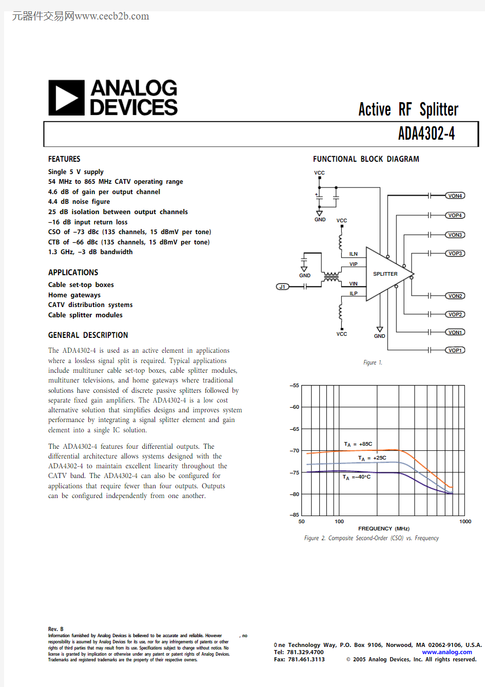
The ADA4302-4 is used as an active element in applications where a lossless signal split is required. Typical applications include multituner cable set-top boxes, cable splitter modules, multituner televisions, and home gateways where traditional solutions have consisted of discrete passive splitters followed by separate fixed gain amplifiers. The ADA4302-4 is a low cost alternative solution that simplifies designs and improves system performance by integrating a signal splitter element and gain element into a single IC solution.
The ADA4302-4 features four differential outputs. The differential architecture allows systems designed with the ADA4302-4 to maintain excellent linearity throughout the CATV band. The ADA4302-4 can also be configured for applications that require fewer than four outputs. Outputs can be configured independently from one another.
FUNCTIONAL BLOCK DIAGRAM
5
1
7
-
1
6
Figure 1.
FREQUENCY (MHz)
C
S
O
(
d
B
c
)
–55
–85
501000
5
1
7
-
8–70
100
–60
–65
–75
–80
Figure 2. Composite Second-Order (CSO) vs. Frequency
ADA4302-4
Rev. B | Page 2 of 12
TABLE OF CONTENTS
Features..............................................................................................1 Applications.......................................................................................1 General Description.........................................................................1 Functional Block Diagram..............................................................1 Revision History...............................................................................2 Specifications.....................................................................................3 Absolute Maximum Ratings............................................................4 ESD Caution..................................................................................4 Pin Configuration and Function Descriptions.............................5 Typical Performance Characteristics..............................................6 Applications........................................................................................8 Circuit Description.......................................................................8 Evaluation Boards.........................................................................8 RF Layout Considerations............................................................8 Power Supply..................................................................................8 Outline Dimensions.......................................................................11 Ordering Guide.. (11)
REVISION HISTORY
9/05—Rev. SpA to Rev. B
Updated Format..................................................................Universal Changes to Circuit Description Section........................................8 5/05—Rev. Sp0 to Rev. SpA
Changes to Format.............................................................Universal Changes to Features..........................................................................1 Changes to Figure 1 and Figure 2...................................................1 Changes to Table 1............................................................................3 Changes to Figure 4 and Figure 5...................................................6 Changes to Applications Section....................................................8 10/04—Revision Sp0: Initial Version
ADA4302-4
Rev. B | Page 3 of 12
SPECIFICATIONS
V CC = 5 V , R IN = R L = 75 Ω, T A = 25°C, unless otherwise noted. The ADA4302-4 is characterized using a balun 1 at the input. Table 1.
Parameter Conditions
Min Typ Max Unit
DYNAMIC PERFORMANCE Bandwidth (?3 dB) 1300 MHz Specified Frequency Range 54 865 MHz Gain (S21) f = 100 MHz 3.5 4.6 5.7 dB Gain Flatness f = 865 MHz 1 dB NOISE/DISTORTION PERFORMANCE Composite Triple Beat (CTB) 135 Channels, 15 dBmV/Channel, f = 103.25 MHz ?66 ?62 dBc Composite Second-Order (CSO) 135 Channels, 15 dBmV/Channel, f = 103.25 MHz ?73 ?67 dBc
Cross Modulation (CXM) 135 Channels, 15 dBmV/Channel, 100% modulation
@ 15.75 kHz, f = 103.25 MHz
?67 ?64 dBc Output IP3 f 1 = 97.25 MHz, f 2 = 103.25 MHz 23 dBm Output IP2 f 1 = 97.25 MHz, f 2 = 103.25 MHz 65 dBm Noise Figure @ 54 MHz 4.1 4.4 dB @ 550 MHz 4.4 4.7 dB @ 865 MHz 5.0 5.8 dB INPUT CHARACTERISTICS Input Return Loss (S11) Referenced to 75 Ω @ 54 MHz ?16 ?14 dB @ 550 MHz ?16 ?11 dB @ 865 MHz ?18 ?11 dB Output-to-Input Isolation (S12) Any output, 54 MHz to 865 MHz ?35 ?33 dB OUTPUT CHARACTERISTICS Output Return Loss (S22) Referenced to 75 Ω @ 54 MHz ?11 ?9 dB @ 550 MHz ?12.5 ?10 dB @ 865 MHz ?14 ?11.5 dB Output-to-Output Isolation Between any two outputs, 54 MHz to 865 MHz ?25 dB 1 dB Compression Output referred, f = 100 MHz 8 dBm POWER SUPP L
Y Nominal Supply Voltage 5 V Quiescent Supply Current
215 240 mA
1
M/A-COM MABAES0029.
ADA4302-4
Rev. B | Page 4 of 12
ABSOLUTE MAXIMUM RATINGS
Table 2.
Parameter Rating Supply Voltage
5.5 V
Storage Temperature Range ?65°C to +125°C Operating Temperature Range
?40°C to +85°C Lead Temperature (Soldering 10 sec) 300°C Junction Temperature
150°C
Stresses above those listed under Absolute Maximum Rating may cause permanent damage to the device. This is a stress rating only; functional operation of the device at these or any other conditions above those indicated in the operational
section of this specification is not implied. Exposure to absolute maximum rating conditions for extended periods may affect device reliability.
ESD CAUTION
ESD (electrostatic discharge) sensitive device. Electrostatic charges as high as 4000 V readily accumulate on the human body and test equipment and can discharge without detection. Although this product features proprietary ESD protection circuitry, permanent damage may occur on devices subjected to high energy electrostatic discharges. Therefore, proper ESD precautions are recommended to avoid performance
degradation or loss of functionality.
ADA4302-4
Rev. B | Page 5 of 12
PIN CONFIGURATION AND FUNCTION DESCRIPTIONS
VOP4VON4VCC VCC ILN 13VCC 14VOP315VON312VCC 11ILP
6G N D 7V I P 8G N D C 10
G N D
9V I N 18G N D 19V O P 120V O N 117V O N 216
V O P 2
05017-001
Figure 3. 20-Lead LFCSP_VQ Pin Configuration
Table 3. Pin Function Descriptions
Pin No. Mnemonic Description
1 VOP4 Positive Output 4 2
VON4 Negative Output 4 3, 4, 12, 13 VCC Supply Pin 5
ILN Bias Pin 6, 10, 18 GND Ground
7 VIP Positive Input 8 GNDC Ground
9 VIN Negative Input 11 ILP Bias Pin
14 VOP3 Positive Output 3 15 VON3 Negative Output 3 16 VOP2 Positive Output 2 17 VON2 Negative Output 2 19 VOP1 Positive Output 1 20
VON1
Negative Output 1
ADA4302-4
Rev. B | Page 6 of 12
TYPICAL PERFORMANCE CHARACTERISTICS
FREQUENCY (MHz)
C S O (d B c )
–55
–85
50
1000
–70
100
–60
–65
–75
–80
Figure 4. Composite Second-Order (CSO) vs. Frequency
FREQUENCY (MHz)
C T B (d B c )
–55
–75
50
1000
100
–60
–65
–70
Figure 5. Composite Triple Beat (CTB) vs. Frequency
FREQUENCY (MHz)
C X M (d B c )
–55
–60
–70
–65
–75
Figure 6. Cross Modulation (CXM) vs. Frequency FREQUENCY (MHz)
N O I S E F I
G U R E (d B )
7
6
5
4
3
205017-006
Figure 7. Noise Figure vs. Frequency
FREQUENCY (MHz)
O U T P U T I P 2 (d B m )
90
70
80
40
50
60
3050
100
1000
05017-012
Figure 8. Output IP2 vs. Frequency
FREQUENCY (MHz)
O U T P U T I P 3 (d B m )
25
20
5
10
15
050
100
1000
05017-013
Figure 9. Output IP3 vs. Frequency
ADA4302-4
Rev. B | Page 7 of 12
FREQUENCY (MHz)
G A I N (d B )
10
5
–5
–10
–15
–20
Figure 10. AC Response (S21)
FREQUENCY (MHz)
I S O L A T I O N (d B )
–10–20–30–40–50
50
100
1000
05017-005
Figure 11. Output-to-Input Isolation vs. Frequency (S12)
FREQUENCY (MHz)
I S O L A T I O N (d B )
–10
–5
–15–20–25–30–35
50
100
1000
05017-007
Figure 12. Output-to-Output Isolation vs. Frequency FREQUENCY (MHz)
I N P U T R E T U R N L O S S (d B )
–5–10
–15
–20
–25
50
100
1000
05017-002
Figure 13. Input Return Loss vs. Frequency (S11)
FREQUENCY (MHz)
O U T P U T R E T U R N L O S S (d B )
–5
–10
–15
–20
–25
50
100
1000
05017-004
Figure 14. Output Return Loss vs. Frequency (S22)
TEMPERATURE (°C)
Q U I E S C E N T S U P P L Y C U R R E N T (m A )
240235210
205
220215225230200–60
–40–20
020*********
05017-011
Figure 15. Quiescent Supply Current vs. Temperature
ADA4302-4
Rev. B | Page 8 of 12
APPLICATIONS
The ADA4302-4 active splitter is primarily intended for use in the downstream path of television set-top boxes (STBs) that contain multiple tuners. It is located directly after the diplexer in a CATV customer premise unit. The ADA4302-4 provides a differential input and four differential outputs that allow the delivery of the RF signal to up to four different signal paths. These paths can include, but are not limited to, a main picture tuner, the picture-in-picture (PIP) tuner, a digital video recorder (DVR), and a cable modem (CM).
The differential nature of the ADA4302-4 allows it to provide composite second-order (CSO) and composite triple beat
(CTB) products that are ?73 dBc and ?66 dBc, respectively. The use of the SiGe process also allows the ADA4302-4 to achieve a noise figure (NF) that is less than 5 dB.
CIRCUIT DESCRIPTION
The ADA4302-4 has a low noise buffer amplifier that is followed by four parallel amplifiers. This arrangement
provides 4.6 dB of gain relative to the RF signal present at the differential inputs of the active splitter. The input and each output must be properly matched to a differential 75 Ω environment in order for distortion and noise performance to match the data sheet specifications. If needed, baluns to convert to single-ended operation can be used. The M/A-COM MABAES0029 is recommended for the input balun and the Mini-Circuit? TC1-1-13M-2 is recommended for the output balun. AC coupling capacitors of 0.01 μF are recommended for all inputs and outputs.
Two 1 μH RF chokes, L1 and L2 (Coilcraft chip inductor
0805LS-102X), are used to correctly bias internal nodes of the ADA4302-4 by connecting them between the 5 V supply and ILN and ILP , respectively.
EVALUATION BOARDS
There are two evaluation boards for the ADA4302-4, a single-ended output board (ADA4302-4 EBSE) and a differential output board (ADA4302-4 EBDI). The single-ended output board has an input balun that converts a signal from a single-ended source to a differential signal. The differential output board uses the same input balun and allows the output signals to run directly to the board connectors. This allows the differential signals at the ADA4302-4’s outputs to be applied directly to a tuner with differential inputs. The schematics for these evaluation boards can be seen in Figure 16 and Figure 17, respectively.
Each board has place holders to properly terminate the unused outputs, if needed. On the single-ended output board, they are designated R15 through R18, and 75 Ω resistors should be used here (see Figure 16). On the differential output board, 37.5 Ω resistors should be used for R1, R2, and R4 through R9 when their respective outputs are not in use (see Figure 17).
RF LAYOUT CONSIDERATIONS
Appropriate impedance matching techniques are mandatory when designing a circuit board for the ADA4302-4. Improper characteristic impedances on traces can cause reflections that can lead to poor linearity. If the stage following the ADA4302-4 is a single-ended load with a 75 Ω impedance, then a balun should be used. The characteristic impedance of the signal trace from each output of a differential pair to the output balun should be 37.5 Ω. In the case of the differential output evaluation board, the output traces should also have a characteristic impedance of 37.5 Ω.
POWER SUPPLY
The 5 V supply should be applied to each of the VCC pins and RF chokes via a low impedance power bus. The power bus should be decoupled to ground using a 10 μF tantalum
capacitor and a 0.01 μF ceramic chip capacitor located close to the ADA4302-4. In addition, the VCC pins should be decoupled to ground with a 0.01 μF ceramic chip capacitor located as close to each of the pins as possible. Pin 3 and Pin 4 can share one capacitor, and Pin 12 and Pin 13 can share one capacitor.
ADA4302-4
Figure 16. Single-Ended Output Evaluation Board
Table 4. ADA4302-4ACPZ-EBSE Bill of Materials (BOM)
Quantity Description Reference
2 Coilcraft 0805LS-102X Chip Inductor L1, L2
4 Mini-Circuit TC1-1-13M-2 Transformer T1 to T4
1 M/A-COM MABAES0029 Transformer T5
13 MLCC, 0.01 μF, C402 C1 to C11, C14, C19
1 Tantalum, 10 μF, B Size C13
1 ADA4302-4ACPZ DUT
5 SMA Connectors J1, P1 to P4
9 Impedance Matching Resistors, Insert as Needed R2, R3, R6, R8, R10, R15 to R18
Rev. B | Page 9 of 12
ADA4302-4
Rev. B | Page 10 of 12
0.01μF
05017-014
Figure 17. Differential Output Evaluation Board
Table 5. ADA4302-4ACPZ-EBDI Bill of Materials (BOM)
Quantity Description
Reference 2 Coilcraft 0805LS-102X Chip Inductor L1, L2 1 M/A-COM MABAES0029 Transformer T5
13 MLCC, 0.01 μF, C402 C1 to C11, C14, C19 1 Tantalum, 10 μF, B size C13 1 ADA4302-4ACPZ DUT
9 SMA Connectors
J1, P1VDN to P4VDN, P1VDP to P4VDP 8
Impedance Matching Resistors, Insert as Needed
R1, R2, R4 to R9
ADA4302-4
Rev. B | Page 11 of 12
OUTLINE DIMENSIONS
0.300.230.18
BSC
1.000.850.80PLANE
COPLANARITY
0.08
0.60COMPLIANT TO JEDEC STANDARDS MO-220-VGGD-1
Figure 18. 20-Lead Lead Frame Chip Scale Package [LFCSP_VQ]
4 mm × 4 mm Body, Very Thin Quad
(CP-20-1)
Dimensions shown in millimeters
ORDERING GUIDE
Model
Ordering Quantity Temperature Range Package Description Package Option ADA4302-4ACP-REEL 5,000 ?40°C to +85°C 20-Lead LFCSP_VQ CP-20-1 ADA4302-4ACP-RL7 1,500 ?40°C to +85°C 20-Lead LFCSP_VQ CP-20-1 ADA4302-4ACPZ-RL 15,000 ?40°C to +85°C 20-Lead LFCSP_VQ CP-20-1 ADA4302-4ACPZ-RL711,500 ?40°C to +85°C 20-Lead LFCSP_VQ CP-20-1 ADA4302-4ACPZ-R21250 ?40°C to +85°C 20-Lead LFCSP_VQ
CP-20-1 ADA4302-4ACPZ-EBSE 2 1 Single-Ended Evaluation Board
ADA4302-4ACPZ-EBDI 2
1 Differential Output Evaluation Board
1 Z = Pb-free part.
2
Evaluation board contains Pb-free part.
ADA4302-4
Rev. B | Page 12 of 12
NOTES
? 2005 Analog Devices, Inc. All rights reserved. Trademarks and registered trademarks are the property of their respective owners.
D05017–0–9/05(B)