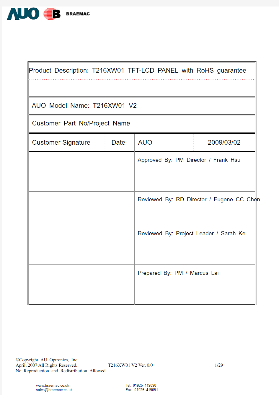
Product Description: T216XW01 TFT-LCD PANEL with RoHS guarantee
AUO Model Name: T216XW01 V2
Customer Part No/Project Name:
Customer Signature Date AUO 2009/03/02
Approved By: PM Director / Frank Hsu
Reviewed By: RD Director / Eugene CC Chen
Reviewed By: Project Leader / Sarah Ke
Prepared By: PM / Marcus Lai
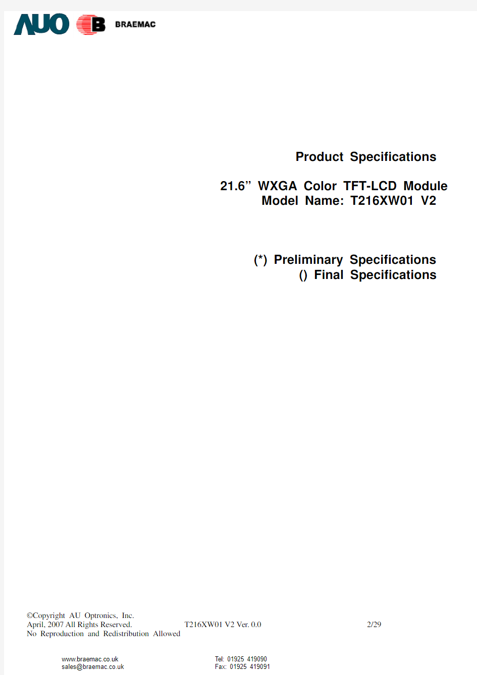
Product Specifications 21.6” WXGA Color TFT-LCD Module
Model Name: T216XW01 V2 (*) Preliminary Specifications
() Final Specifications
Contents
No ITEM COVER CONTENTS RECORD OF REVISIONS
1 GENERAL DESCRIPTION
2
ABSOLUTE MAXIMUM RATINGS
3 ELECTRICAL SPECI F ICATIONS 3-1 ELECTRICAL CHARACTERISTICS 3-2 INTER F
ACE CONNECTIONS 3-3 SIGNAL TIMING SPECI F ICATIONS 3-4 SIGNAL TIMING WAVE F
ORMS 3-5 COLOR INPUT DATA REFERENCE 3-6
POWER SEQUENCE for LCD 4 OPTICAL SPECI F ICATIONS
5 MECHANICAL CHARACTERISTICS 5-1 F RONT VIEW 5-2 REAR VIEW
6 RELIABILITY
7 INTERNATIONAL STANDARDS 7-1 SA F
ETY 7-2 EMC 7-3 GREEN 8 PACKING
8-1 PACKING INSTRUCTION 8-2 SHIPPING LABEL 8-3 CARTON LABEL 9 PRECAUTIONS
9-1 MOUNTING PRECAUTIONS 9-2 OPERATING PRECAUTIONS 9-3 ELECTROSTATIC DISCHARGE CONTROL 9-4 PRECAUTIONS FOR STRONG LIGHT EXPOSURE 9-5 STORAGE
9-6 HANDLING PRECAUTIONS FOR PROTECTION FILM
Record Revision
Version Date No Old Description New Description Remark
irst Draft
0.0 2009/03/02
F
1. General Description
This specification applies to the 21.6 inch Color TFT-LCD Module T216XW01. This LCD module has a TFT active matrix type liquid crystal panel with 1,366x768 pixels, and the diagonal size is 21.6 inches. This module supports 1,366x768 XGA-WIDE mode (Non-interlace).
Each pixel is divided into Red, Green and Blue sub-pixels or dots which are arranged in vertical stripes. Gray
scale or the brightness of the sub-pixel color is determined with an 8-bit gray scale signal for each dot.
The T216XW01 has been designed to apply to 8-bit and 1 channel LVDS interface method. It is intended to support displays where high brightness, wide viewing angle, high color saturation, and high color depth are
very important.
This module is not equipped with inverter board for backlight.
* General Information
Unit
Note Item Specification
Active Screen Size 21.6 Inch
Display Area 477.417 (H) x 268.416 (V) mm
Outline Dimension 523 (H) ? 315 (V) ? 29 (D) mm w/o
Inverter
Resolution 1,366 x 768 pixel
Pixel Pitch 0.3495 mm
Pixel Arrangement RGB vertical stripe
Display mode Normally Black
Display Colors 16.7M (8-bit for R,G,B) color
Typical White Luminance 350 @ 9.5 mA [cd/m2]
Surface Treatment AG, Haze=11%, 3H
compliance
Green RoHS
2. Absolute Maximum Ratings
The following are maximum values which, if exceeded, may cause faulty operation or damage to the unit.
Max
Note
Unit
Item Symbol
Min
Logic/LCD Drive Voltage Vdd -0.3 6 [Volt] 1
Input Voltage of Signal Vin -0.3 3.6 [Volt] 1
Operating Temperature TOP 0 +50 [o C] 2
Operating Humidity HOP 10 90 [%RH] 2
Storage Temperature TST -20 +60 [o C] 2
Storage Humidity HST 10 90 [%RH] 2
Note
1, Duration = 50 msec
2, Maximum Wet-Bulb should be 39 and
кno condensation. The relative humidity must not exceed 90%
non-condensing at temperatures of 40 or less. At temperatures greater than 40, the w
ккet bulb
temperature must not exceed 39.
к
3, Surface temperature is measured at 50к Dry condition
3. Electrical Specification
The T216XW01 requires two power inputs. One is employed to power the LCD electronics and to drive the TFT array and liquid crystal. An inverter typically generates the second input, which powers the CCFL.
3-1 Electrical Characteristics
Values
Parameter Symbol
Min Typ Max
Unit Notes Power Supply Input Voltage Vcc 4.5 5.0 5.5 Vdc 1
Power Supply Input Current Icc?- 0.8
1.0 A 2
Power Consumption Pc - 4.0 5.0 Watt 2 LCD
Inrush Current I RUSH - - 3
Apeak 3
Differential Input High Threshold Voltage VTH - - 100
mV 4
Differential Input Low Threshold Voltage VTL -100 - - mV 4
LVDS
Interface
Common Input Voltage VCIM 0.6 1.25 1.8 V 4
Input High Threshold Voltage
VIH
(High)
2.0
3.3 3.6 Vdc
CMOS
Interface
Input Low Threshold Voltage
VIL
(Low)
0 - 0.8
Vdc
Life Time 50,000 - - 5,6,7,8 Note :
1. The ripple voltage should be controlled under 10% of V CC
2. Vcc=5.0V, =
v
f60Hz, fCLK=81.5Mhz , 25к, Test Pattern : White Pattern
3. Measurement condition:
4. VCIM = 1.25V
5. Take the life time and brightness for example, the performance of the lamp in LCD panel is extremely
influenced by the characteristics of the DC-AC Inverter. All the parameters of the inverter should be carefully designed to avoid producing too much leakage current from high-voltage output of the inverter. Please make sure unwanted lighting caused by the mismatch of the lamp and the inverter (no lighting, flicker, etc) never occurs. After confirmation, the LCD panel should be operated in the same condition as installed in your instrument.
6. Do not attach a conducting tape to lamp connecting wire. If the lamp wire attach to conducting tape, the TFT-LCD Module has a low luminance and the inverter has abnormal action because leakage current occurs between lamp wire and conducting tape.
7. The relative humidity must not exceed 80% non-condensing at temperatures of 40 or less. At
кtemperatures greater than 40, the wet bulb temperature must not exceed 39. When operate at low ккtemperatures, the brightness of CCFL will drop and the life time of CCFL will be reduced.
8. Specified values are for a single lamp only which is aligned horizontally. The lifetime is defined as the
time which luminance of the lamp is 50% compared to its original value. [Operating condition: Continuous operating at Ta = 25±2]к
0V
3-2 Interface Connections?
3-2-1 LCD connector (CN1): Starconn 093G30-B0001A-1
Pin No Symbol Description Note
1 Reserved Open AUO internal test pin
2 Reserved Open AUO internal test pin
3 Reserved Open AUO internal test pin
Ground
4 GND
5 Rx0- LVDS Channel 0 [Polarity: Negative]
6 Rx0+ LVDS Channel 0 [Polarity: Positive]
Ground
7 GND
8 Rx1- LVDS Channel 1 [Polarity: Negative]
9 Rx1+ LVDS Channel 1 [Polarity: Positive]
Ground
10 GND
11 Rx2- LVDS Channel 2 [Polarity: Negative]
12 Rx2+ LVDS Channel 2 [Polarity: Positive]
Ground
13 GND
14 RXCLK- LVDS Clock [Polarity: Negative]
15 RXCLK+ LVDS Clock [Polarity: Positive]
Ground
16 GND
17 Rx3- LVDS Channel 3 [Polarity: Negative]
18 Rx3+ LVDS Channel 3 [Polarity: Positive]
Ground
19 GND
20 Reserved Open AUO internal test pin
21 LVDS Option* Low for JEIDA, High/Open for NS
Open
22 Reserved
Ground
23 GND
Ground
24 GND
Ground
25 GND
26 Vdd (+5V) 5V, DC, Regulated
27 Vdd (+5V) 5V, DC, Regulated
28 Vdd (+5V) 5V, DC, Regulated
29 Vdd (+5V) 5V, DC, Regulated
30 Vdd (+5V) 5V, DC, Regulated
NoteΚ
1, All GND (ground) pins should be connected together and should also be connected to the LCD’s metal frame.
2, All Vcc (power input) pins should be connected together.
* LVDS Option =L (GND)? JETDA Format
Clock
RIN0+
RIN0-
RIN1+
RIN1-
RIN2+
RIN2-
RIN3+
RIN3-
* LVDS Option = H (3.3V) or N.C.? NS Format
Clock
RIN0+
RIN0-
RIN1+
RIN1-
RIN2+
RIN2-
RIN3+
RIN3-
3-2-2 Backlight Electrical Specification
?
Description Min Typ Max Unit Condition/Note
1 Operating Voltage Vo 1060.
2 1178 1295.8 Vrms 1. Dimming range is set 100% 2. Base on lamp specification, for each lamp need to be
applied at least minimum
operating voltage to ensure each lamp can be normally worked!
2 Operating Current Io 8.0 9.5 10 mArms 1. Dimming range is set 100% 2. Base on lamp specification, for each lamp need to be
applied at least minimum
operating current to ensure each lamp can be normally worked!
3 BL Total Power Dissipation PBL 30 36 Watt 1. Dimming range is set 100%. 2. In order to get typical light out, the backlight need to be
applied typical power.
3. Input power of JIG BD is about 75 W (typ.) by AUO’s measurement!
At 0к 1860 2060 - 4 Striking Voltage At 25к Vstrike 1550 1750 -
Vrms 1. Base on lamp specification,
to ensure each lamp can be
normally ignited, need to
apply at least minimum striking voltage to each lamp 5 Striking Time Ts 1000 - 1500 msec 1. To ensure each lamp can be normally ignited, each lamp
need to be applied at least
minimum striking voltage
during minimum striking time. 6 Operating F requency fo - 58 - kHz
1. Operating frequency is set by customers.
2. Need to double confirm display quality.(*)
.7 PWM Operating Frequency F_PWM 140 180 240 Hz
1. PWM frequency is set by customers.
2. Need to double confirm display quality.(*) 8 PWM Dimming Duty Ratio D_PWM 10 - 100 %
Note 2.
Note 3. Duty ratio definition.
9 Lamp Type U type ?
10 Number of Lamps
3
pcs
Note :
1, Ta=25±5, Turn on for 45minutes к
2, When PWM dimming ratio is operated within recommend value, backlight can be ensured that there is no flicker and uniformity issue and display quality of panel can be normally display! When PWM dimming ration is operated less than recommend value, backlight need to be double confirmed display quality. LIPS need to be double confirmed feedback signal and all protection function!
3, Duty ratio definition:
3-2-3 Lamp specification
Note
1, The above characteristics are measured under the conditions: Ambient temperature: 25±2,
к
Relative Humidity: 65±20%RH.
±).
(unsymmetrical ratio is less than 10%, crest factor within10%
3-2-4 Input Interface for LIPS board
CN1: EL7H001ZZ2 (Manufactured by JAE)
3-3 Signal Timing Specifications
This is the signal timing required at the input of the User connector. All of the interface signal timings should be satisfied with the following specifications for the proper operation. * Timing Table
Signal Item Symbol Min. Typ. Max. Unit
Period Tv 776 810 1,015 Th
Active Tdisp(v) 768 Th Vertical Section
Blanking Tblk (v)
8
42
247
Th
Period Th 1,414 1,648 2,000 Tclk Active Tdisp(h)
1,366 Tclk Horizontal
Section Blanking Tblk (h) 48 282 634 Tclk LVDS Clock
Frequency Fclk (1/Tclk)
50 80 86 MHz Vertical
Frequency
F requency F v 47 60 63 Hz Horizontal Frequency
F requency F h 43
48
53
kHz
Note Κ
1, CLK signal input must be valid while power supply is applied.
2, Display position is specific by the rise of DE signal only. Horizontal display position is specified by the falling edge of 1st
CLK right after the rise of DE, is displayed on the left edge of the screen. Vertical display position is specified by the rise of DE after a “Low” level period equivalent to eight times of horizontal period. The 1st
data corresponding to one horizontal line after the rise of DE is displayed at the top line of screen.
3, If a period of DE “High” is less than 1,366 CLK or less than 768 lines, the rest of the screen displays black. 4, The display position does not fit to the screen if a period of DE “High” and the effective data period do not synchronize with each other.
3-4 Signal Timing Waveforms
CLK
DE
RG
3-5 Color Input Data Reference
The brightness of each primary color (red, green and blue) is based on the 8 bit gray scale data input for the color. The higher the binary input, the brighter the color. The table below provides a reference for color versus data input.
* COLOR DATA REFERENCE
Input Color Data
RED MSB LSB GREEN MSB LSB BLUE
MSB LSB
Color
R7 R6 R5 R4 R3 R2 R1 R0 G7 G6 G5 G4 G3 G2 G1 G0 B7 B6 B5 B4 B3 B2 B1 B0 Black(L0) 0 0 0 0 0 0 0 0 0 0 0 0 0 0 0 0 0 0 0 0 0 0 0 0 Red(255)
1 1 1 1 1 1 1 1 0 0 0 0 0 0 0 0 0 0 0 0 0 0 0 0 Green(255) 0 0 0 0 0 0 0 0 1 1 1 1 1 1 1 1 0 0 0 0 0 0 0 0 Blue(255) 0 0 0 0 0 0 0 0 0 0 0 0 0 0 0 0 1 1 1 1 1 1 1 1 Cyan 0 0 0 0 0 0 0 0 1 1 1 1 1 1 1 1 1 1 1 1 1 1 1 1 Magenta 1 1 1 1 1 1 1 1 0 0 0 0 0 0 0 0 1 1 1 1 1 1 1 1 Yellow 1 1 1 1 1 1 1 1 1 1 1 1 1 1 1 1 0 0 0 0 0 0 0 0
Basic Color
White(L255) 1 1 1 1 1 1 1 1 1 1 1 1 1 1 1 1 1 1 1 1 1 1 1 1
RED(000)
0 0 0 0 0 0 0 0 0 0 0 0 0 0 0 0 0 0 0 0 0 0 0 0 RED(001) 0 0 0 0 0 0 0 1 0 0 0 0 0 0 0 0 0 0 0 0 0 0 0 0 ----
RED(254) 1 1 1 1 1 1 1 0 0 0 0 0 0 0 0 0 0 0 0 0 0 0 0 0
RED
RED(255)
1 1 1 1 1 1 1 1 0 0 0 0 0 0 0 0 0 0 0 0 0 0 0 0
GREEN(000) 0 0 0 0 0 0 0 0 0 0 0 0 0 0 0 0 0 0 0 0 0 0 0 0
GREEN(001) 0 0 0 0 0 0 0 0 0 0 0 0 0 0 0 1 0 0 0 0 0 0 0 0
---- GREEN(254) 0 0 0 0 0 0 0 0 1 1 1 1 1 1 1 0 0 0 0 0 0 0 0 0
GREEN
GREEN(255) 0 0 0 0 0 0 0 0 1 1 1 1 1 1 1 1 0 0 0 0 0 0 0 0 BLUE(000)
0 0 0 0 0 0 0 0 0 0 0 0 0 0 0 0 0 0 0 0 0 0 0 0 BLUE(001)
0 0 0 0 0 0 0 0 0 0 0 0 0 0 0 0 0 0 0 0 0 0 0 1 ------- BLUE(254)
0 0 0 0 0 0 0 0 0 0 0 0 0 0 0 0 1 1 1 1 1 1 1 0 BLUE
BLUE(255) 0 0 0 0 0 0 0 0 0 0 0 0 0 0 0 0 1 1 1 1 1 1 1 1
3-6 Power Sequence
Values
Parameter
Min. Typ. Max.
Unit
t1 0.4 - 30 ms t2 0.1 - 50 ms t3 200 - - ms t4 10 - - ms t5 0.1 - 50 ms t6 - - 300 ms
t7 500 -
- ms
Apply the lamp voltage within the LCD operating range. When the backlight turns on before the LCD operation or the LCD turns off before the backlight turns off, the display may momentarily become abnormal. Caution Κ
The above on/off sequence should be applied to avoid abnormal function in the display. In case of handling, make sure to turn off the power when you plug the cable into the input connector or pull the cable out of the connector.
LVDS Data & CLK
Power Supply for LCD (Vdd)
Power for LAMP
4. Optical Specification
Optical characteristics are determined after the unit has been ‘ON’ and stable for approximately 30 minutes in a dark environment at 25к. The values specified are at an approximate distance 50cm from the LCD surface at a viewing angle of ? and ?equal to 0?.
Parameter
Symbol Min. Typ. Max. Unit Note Contrast Ratio
CR 2,000 2,500 1 Surface Luminance, white LWH 300 350 cd/ф 2 Luminance Variation ?WHITE
9 p
1.3 3 Response Time T ? 6.5 ms 4
Color Gamut
72
%
RED R X 0.640
R Y 0.330
GREEN G X 0.290
G Y 0.600 BLUE B X 0.150 B Y 0.060 WHITE W X 0.285
Color Coordinates
W Y Typ.-0.03 0.293
Typ.+0.03
x axis, right(?=0?)
?r 65 88 Degree 5
x axis, left(?=180?)
?l 65 88 Degree 5 y axis, up(?=90?)
?u 55 88 Degree 5 Viewing Angle by ELDIM y axis, down (?=0?)
?d
55 88
Degree 5
PR880 or equivalent
V
H
V/6
V/2
Note Κ
1, Contrast Ratio (CR) is defined mathematically as:
Surface Luminance of L on1
Contrast Ratio=
Surface Luminance of L off1
2, Surface luminance is luminance value at point 1 across the LCD surface 50cm from the surface with all pixels displaying white. F rom more information see F IG 4-2. When I BL = 57mA, L WH =350cd/ф(typ.) L WH =Lon1, Where Lon1 is the luminance with all pixels displaying white at center 1 location.
4, Response time T?is the average time required for display transition by switching the input signal for five luminance ratio (0%,25%,50%,75%,100% brightness matrix) and is based on f v=60Hz to optimize.
5, Viewing angle is the angle at which the contrast ratio is greater than 10. The angles are determined for the horizontal or x axis and the vertical or y axis with respect to the z axis which is normal to the LCD surface. For more information see FIG 4-5.
Fig.4-4 Viewing Angle Definition