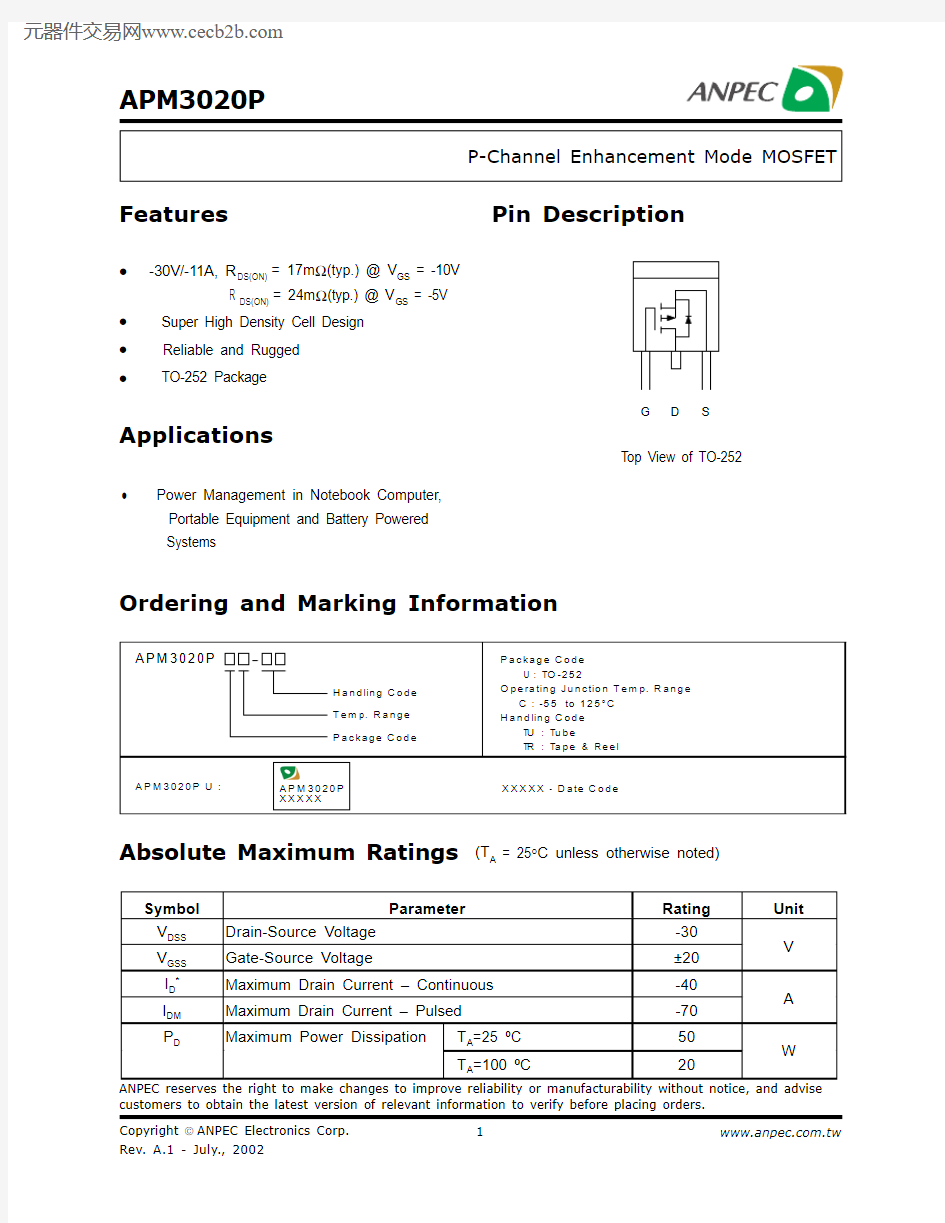

customers to obtain the latest version of relevant information to verify before placing orders.Pin Description
Ordering and Marking Information
Features
Applications
? Power Management in Notebook Computer,
Portable Equipment and Battery Powered Systems
? -30V/-11A, R DS(ON) = 17m ?(typ.) @ V GS = -10V
R DS(ON) = 24m ?(typ.) @ V GS = -5V
? Super High Density Cell Design ? Reliable and Rugged ? TO-252 Package
Absolute Maximum Ratings (T A = 25°C unless otherwise noted)
A P M 3020P
H a n d lin g C o d e T e m p. R a n g e P a c ka g e C o d e
P a c k a g e C o d e U : T O -252
O p e ra tin g J u n c tio n T e m p. R a n g e C : -55 to 125°C H a n d lin g C o d e T U : T u b e
T R : T a p e & R e e l
A P M 3020P U :
A P M 3020P X X X X X
X X X X X - D a te C o d e
Top View of TO-252
G
D
S
Electrical Characteristics (T A = 25°C unless otherwise noted)
Absolute Maximum Ratings (T A = 25°C unless otherwise noted)
Notes
a
: Guaranteed by design, not subject to production testing b
: Pulse test ; pulse width ≤ 500μs, duty cycle ≤ 2%
012345
0246810
10
20
30
4050
0510********
-50
-250255075100125150
0.000.250.500.751.001.251.50
Typical Characteristics
Output Characteristics
-V DS -Drain-to-Source Voltage (V)-I D S -D r a i n C u r r e n t (A )
Transfer Characteristics
-V GS -Gate-to-Source Voltage (V)
-I D S -D r a i n C u r r e n t (A )
Threshold Voltage vs. Junction T emperature
T j -Junction T emperature (°C)-V G S (t h )-T h r e s h o l d V o l t a g e (V )(N o r m a l i z e d )
On-Resistance vs. Drain Current
-I DS -Drain Current (A)
R D S (O N )-O n -R e s i s t a n c e (?)
0510********
010203040
-50
-250255075100125150
0246810
Typical Characteristics Cont.
On-Resistance vs. Gate-to-Source Voltage
R D S (O N )-O n -R e s i s t a n c e (?)
-V GS - Gate-to-Source Voltage (V)
On-Resistaence vs. Junction T emperature
R D S (O N )-O n -R e s i s t a n c e (?)(N o r m a l i z e d )
T j -Junction Temperature (°C)
Gate Charge
Q G -T otal Gate Charge (nC)
-V G S -G a t e -t o -S o u r c e V o l t a g e (V )
Capacitance Characteristics
-V DS -Drain-to-Source Voltage (V)
C -C a p a c i t a n c e (p F )
10
-5
10
-4
10
-3
10
-2
10
-1
10
10
1
0.010.1
1
10
-510
-4
10
-3
10
-2
10
-1
10
10
1
0500
10001500
2000
25003000
0.00.20.40.60.8 1.0 1.2 1.4 1.6 1.8
0.1
1
10
50
Typical Characteristics Cont.
Source-Drain Diode Forward Voltage
-I S D -S o u r c e C u r r e n t (A )
-V SD -Source-to-Drain Voltage (V )
Time (sec)
Single Pulse Power
P o w e r (W )
Square Wave Pulse Duration (sec)
N o r m a l i z e d E f f e c t i v e T r a n s i e n t T h e r m a l I m p e d a n c e
Normalized Transient Thermal Transient Impedence, Junction to Ambient
Packaging Information
TO-252( Reference JEDEC Registration TO-252)
Physical Specifications
Pre-heat temperature
183 C
Peak temperature
Time
°t e m p e r a t u r e
Classification Reflow Profiles
Package Reflow Conditions
Reference JEDEC Standard J-STD-020A APRIL 1999
Reflow Condition (IR/Convection or VPR Reflow)
Reliability test program
Carrier Tape
Cover Tape Dimensions
Customer Service
Anpec Electronics Corp.
Head Office :
5F, No. 2 Li-Hsin Road, SBIP,
Hsin-Chu, T aiwan, R.O.C.
T el : 886-3-5642000
Fax : 886-3-5642050
Taipei Branch :
7F, No. 137, Lane 235, Pac Chiao Rd.,
Hsin Tien City, Taipei Hsien, T aiwan, R. O. C.
T el : 886-2-89191368
Fax : 886-2-89191369