SPI总线
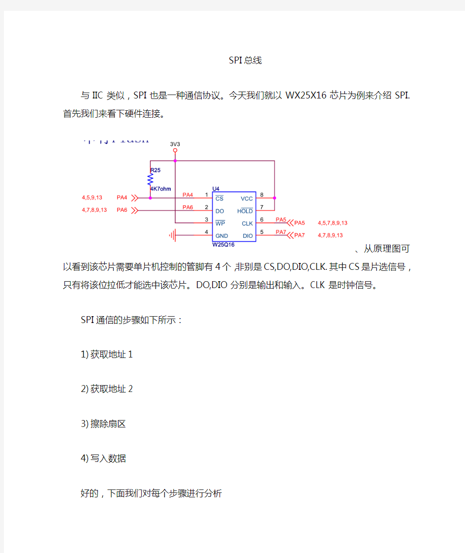
与IIC类似,SPI也是一种通信协议。今天我们就以WX25X16芯片为例来介绍SPI.首先我们来看下硬件连接。
、从原理图可以看到该芯片需要单片机控制的管脚有4个,非别是CS,DO,DIO,CLK.其中CS 是片选信号,只有将该位拉低才能选中该芯片。DO,DIO分别是输出和输入。CLK是时钟信号。SPI通信的步骤如下所示:
1)获取地址1
2)获取地址2
3)擦除扇区
4)写入数据
好的,下面我们对每个步骤进行分析
(1)在对芯片操作前先要对端口及SPI外设进行相应的设置:
/*
函数名:SPI_FLASH_Init(void)
功能:对端口和SPI初始化
输入:无
输出:无
调用:被主函数调用
*/
void SPI_FLASH_Init(void)
{
SPI_InitTypeDef SPI_InitStructure;
GPIO_InitTypeDef GPIO_InitStructure;
/* Enable SPI1 and GPIO clocks */
RCC_APB2PeriphClockCmd(RCC_APB2Periph_GPIOA | RCC_APB2Periph_GPIOD, ENABLE);
/*!< SPI_FLASH_SPI Periph clock enable */
RCC_APB2PeriphClockCmd(RCC_APB2Periph_SPI1, ENABLE);
/*将PA5(CLK)配置成复用推挽输出*/
GPIO_InitStructure.GPIO_Pin = GPIO_Pin_5;
GPIO_InitStructure.GPIO_Speed = GPIO_Speed_50MHz;
GPIO_InitStructure.GPIO_Mode = GPIO_Mode_AF_PP;
GPIO_Init(GPIOA, &GPIO_InitStructure);
/*将PA6(DO)设置成浮空输入*/
GPIO_InitStructure.GPIO_Pin = GPIO_Pin_6;
GPIO_Init(GPIOA, &GPIO_InitStructure);
/将PA7(DIO)设为浮空输入/
GPIO_InitStructure.GPIO_Pin = GPIO_Pin_7;
GPIO_Init(GPIOA, &GPIO_InitStructure);
/将PA4(CS)设为推挽输出/
GPIO_InitStructure.GPIO_Pin = GPIO_Pin_4;
GPIO_InitStructure.GPIO_Mode = GPIO_Mode_Out_PP;
GPIO_Init(GPIOA, &GPIO_InitStructure);
/拉高CS,失能芯片,该语句是宏定义,就是置高PA4/
SPI_FLASH_CS_HIGH();
/* SPI配置/
// W25X16: data input on the DIO pin is sampled on the rising edge of the CLK.
// Data on the DO and DIO pins are clocked out on the falling edge of CLK.
/*将SPI设为全双工模式*/
SPI_InitStructure.SPI_Direction = SPI_Direction_2Lines_FullDuplex;
/*将SPI设为主模式*/
SPI_InitStructure.SPI_Mode = SPI_Mode_Master;
/*将SPI通信的数据大小设为8位*/
SPI_InitStructure.SPI_DataSize = SPI_DataSize_8b;
/*将CLK的高电平设为空闲*/
SPI_InitStructure.SPI_CPOL = SPI_CPOL_High;
/*设置在第二个时钟沿捕获数据*/
SPI_InitStructure.SPI_CPHA = SPI_CPHA_2Edge;
/*指定NSS信号由软件管理*/
SPI_InitStructure.SPI_NSS = SPI_NSS_Soft;
/SPI_BaudRatePrescaler用来定义波特率预分频的值,这个值用以设置发送和接收的SCK时钟/
SPI_InitStructure.SPI_BaudRatePrescaler = SPI_BaudRatePrescaler_4;
/SPI_FirstBit指定了数据传输从高位还是低位开始/
SPI_InitStructure.SPI_FirstBit = SPI_FirstBit_MSB;
/SPI_CRCPolynomial定义了用于CRC值计算的多项式/
SPI_InitStructure.SPI_CRCPolynomial = 7;
SPI_Init(SPI1, &SPI_InitStructure);
/* Enable SPI1 */
SPI_Cmd(SPI1, ENABLE);
}
(2)获取器件地址1
因为SPI总线上可以挂很多的器件,所以首先要获得器件的地址。
获得器件地址的步骤是:拉低CS——>向器件发送获得地址的命令——>连续发送三个任意数据——>在发送第四个任意数据时在DO口上读出器件地址。注意,发送完读地址后,从机会将数据自动传给主机的SPI 数据寄存器中,用户只要到该寄存器中取数就可以了。
好的,既然用到写命令那么我们写来写这两个最基础的程序。
写数据函数:
/************************************************************* ******************
* Function Name : SPI_FLASH_SendByte
* Description : 通过SPI总线发送一字节数据,再通过SPI总线返回一字节数据
* Input : byte ——要发送的数据
* Output : 从机返回的数据
* 调用:被SPI_FLASH_ReadDeviceID调用
************************************************************** *****************/
u8 SPI_FLASH_SendByte(u8 byte)
{
/* 等待SPI发送寄存器里的数据发送结束*/
while(SPI_I2S_GetFlagStatus(SPI1, SPI_I2S_FLAG_TXE) == RESET);
/* 发送数据*/
SPI_I2S_SendData(SPI1, byte);
/* 等待接收完一字节数据*/
while (SPI_I2S_GetFlagStatus(SPI1, SPI_I2S_FLAG_RXNE) == RESET);
/* 返回接收到的数据*/
return SPI_I2S_ReceiveData(SPI1);
}
现在我们再来看看读器件地址函数:
/************************************************************* ******************
* Function Name : SPI_FLASH_ReadDeviceID(void)
* Description : 读器件地址1
* Input : 无
* Output : 无
* 返回: 器件地址
调用:SPI_FLASH_SendByte
************************************************************** *****************/
u32 SPI_FLASH_ReadDeviceID(void)
{
u32 Temp = 0;
/* SPI_FLASH_CS_LOW(),是一个宏定义,就是拉低CS(PA4)*/ SPI_FLASH_CS_LOW();
/*W25X_DeviceID=0XAB,是读器件地址的命令,发送完该命令后连续发三个任意数字,在发第五个任意数后可以读出地址*/
SPI_FLASH_SendByte(0XAB);
SPI_FLASH_SendByte(0XFF);
SPI_FLASH_SendByte(0XFF);
SPI_FLASH_SendByte(0XFF);
/* Read a byte from the FLASH */
Temp = SPI_FLASH_SendByte(0XFF);
/* 失能芯片*/
SPI_FLASH_CS_HIGH();
/*返回器件地址*/
return Temp;
}
像温度传感器一样,WX25X16也有很多的命令,具体的命令看下图:
图5-1
(3)获取器件地址2
获取完地址1后,我们再来获取地址2.读地址2的命令是0X9F,从图5-1中可以看到,发送完0X9F后连续读出3个数据。好的,我们来看看具体的程序:
/********************************************************************
***********
* Function Name : SPI_FLASH_ReadID
* Description : 读器件地址2
* Input : 无
* Output : 无
* 返回: 器件地址2
调用:SPI_FLASH_SendByte
********************************************************************* **********/
u32 SPI_FLASH_ReadID(void)
{
u32 Temp = 0, Temp0 = 0, Temp1 = 0, Temp2 = 0;
/* 拉低CS来使能从机*/
SPI_FLASH_CS_LOW();
/*W25X_JedecDeviceID=0X9F,读取从机地址的命令,发送完命令后可以连续读三个字节的地址*/
SPI_FLASH_SendByte(0X9F);
/* Read a byte from the FLASH */
Temp0 = SPI_FLASH_SendByte(Dummy_Byte);
/* Read a byte from the FLASH */
Temp1 = SPI_FLASH_SendByte(Dummy_Byte);
/* Read a byte from the FLASH */
Temp2 = SPI_FLASH_SendByte(Dummy_Byte);
/* 拉高CS,失能从机*/
SPI_FLASH_CS_HIGH();
/*将三个地址合并*/
Temp = (Temp0 << 16) | (Temp1 << 8) | Temp2;
return Temp;
}
(4)擦除扇区
WX25X16是2M的字节,共分为8页,每页是256个字节的大小。可以采用页写入的方式写入数据。这里需要注意的是,采用页写入时,每写入一个字节的数据地址会自动加1,当写满一页后会从该页的起始位置写起,即覆盖掉已写的数据。如果想写完一页后进入下一页继续写入数据那么就要在写入数据的起始地址上加上256(页的大小就是256),比如我是从0开始写的,写到255时一页写完,那么要在第二页开始写,那么要将写入的地址变成(0+256),这一点大家一定要注意。在写入数据前先要对芯片进行擦除。
芯片的擦除主要有一下几个步骤:
发送写使能命令——>等待写使能命令执行结束——>选中芯片——>发送擦除命令——>发送要擦除的起始地址——>释放芯片——>等待擦除命令执行结束
这里要注意的是,并不是发送任何命令都需要等待命令执行结束的,WX25X16手册规定以下几个操作要等待命令执行结束:
1.数据擦除
2.对状态寄存器写的操作(例如数据写入失能结会改变状
态寄存器中的BUSY位)
首先看发送写使能命令:
/************************************************************** *****************
* Function Name : SPI_FLASH_WriteEnable
* Description : 允许想芯片内写入数据
* Input : None
* Output : None
* Return : None
调用:被SPI_FLASH_SectorErase调用
*************************************************************** ****************/
void SPI_FLASH_WriteEnable(void)
{
/* Select the FLASH: Chip Select low */
SPI_FLASH_CS_LOW();
/* Send "Write Enable" instruction */
SPI_FLASH_SendByte(0X06);
/* Deselect the FLASH: Chip Select high */
SPI_FLASH_CS_HIGH();
}
等待命令执行结束
/************************************************************** *****************
* Function Name : SPI_FLASH_WaitForWriteEnd
* Description : 执行写使能会值位状态寄存器中的BUSY位,只有
BUSY位变为0时说明写使能命令执行完成
* Input : None
* Output : None
* Return : None
*调用:被SPI_FLASH_SectorErase调用
*************************************************************** ****************/
void SPI_FLASH_WaitForWriteEnd(void)
{
u8 FLASH_Status = 0;
/* Select the FLASH: Chip Select low */
SPI_FLASH_CS_LOW();
/* Send "Read Status Register" instruction */
SPI_FLASH_SendByte(0X05);
/* Loop as long as the memory is busy with a write cycle */
do
{
/* Send a dummy byte to generate the clock needed by the FLASH
and put the value of the status register in FLASH_Status variable */
FLASH_Status = SPI_FLASH_SendByte(Dummy_Byte);
}
while ((FLASH_Status & 0X01) == SET); /* Write in progress */
/* Deselect the FLASH: Chip Select high */
SPI_FLASH_CS_HIGH();
}
下面看看数据擦除函数
/*************************************************************** ****************
* Function Name : SPI_FLASH_SectorErase
* Description : Erases the specified FLASH sector.
* Input : SectorAddr: address of the sector to erase.
* Output : None
* Return : None
*调用:SPI_FLASH_WriteEnable() SPI_FLASH_WaitForWriteEnd()
SPI_FLASH_SendByte
**************************************************************** ***************/
void SPI_FLASH_SectorErase(u32 SectorAddr)
{
/* 发送使能写命令*/
SPI_FLASH_WriteEnable();
/*使能写命令是一个写状态寄存器的命令,所以要等待该命令执行完,
才能写其他命令*/
SPI_FLASH_WaitForWriteEnd();
SPI_FLASH_CS_LOW();
/* 发送擦除扇区命令*/
SPI_FLASH_SendByte(0X20);
/* 发送要擦除的起始地址*/
SPI_FLASH_SendByte((SectorAddr & 0xFF0000) >> 16);
/* Send SectorAddr medium nibble address byte */
SPI_FLASH_SendByte((SectorAddr & 0xFF00) >> 8);
/* Send SectorAddr low nibble address byte */
SPI_FLASH_SendByte(SectorAddr & 0xFF);
/* Deselect the FLASH: Chip Select high */
SPI_FLASH_CS_HIGH();
/* 从机的数据手册规定(12页)规定,对于写擦除命令,要等待命令执行完才能执行下一命令*/
SPI_FLASH_WaitForWriteEnd();
}
这里要注意,发送擦除地址时要发送三个8位的地址。
(5)写入数据
由于我们是选择的的页写入的方式,所以这里的程序又点小复杂,大家慢慢看,好好理解。
/**************************************************************
*****************
* Function Name : SPI_FLASH_BufferWrite
* Description : Writes block of data to the FLASH. In this function, the
* number of WRITE cycles are reduced, using Page
WRITE sequence.
* Input : - pBuffer : pointer to the buffer containing the data to
be written to the FLASH.
* - WriteAddr : FLASH's internal address to write to.
* - NumByteToWrite : number of bytes to write to the FLASH.
* Output : None
* Return : None
***************************************************************
****************/
void SPI_FLASH_BufferWrite(u8 *pBuffer,u32 WriteAddr,u16 NumByteToWrite)
{
u8 NumOfPage =0,NumOfSingl =0,Addr =0,count =0,temp =0;
/*Addr记录的数据是用来判断写入的数据是否从页的起始地址开始写,如果Addr =0,则表示从起始地址开始写,SPI_FLASH_PageSize =256*/
Addr =WriteAddr % SPI_FLASH_PageSize;
/*count记录的是从开始写的地址到该页结束处共有多少字节*/
count =SPI_FLASH_PageSize -Addr;
/*NumOfPage指示要写的数据要占几个整页*/
NumOfPage =NumByteToWrite / SPI_FLASH_PageSize;
/*NumOfSingl指示的是要写的数据在写完整页后还剩下的部分*/
NumOfSingl =NumByteToWrite % SPI_FLASH_PageSize;
/*判断是否从页的起始处开始写起,Addr=0说明从起始处写起*/
if(Addr ==0)
{
if(NumOfPage ==0) //说明要写的数据的大小不足1页
{
SPI_FLASH_PageWrite(pBuffer,WriteAddr,NumByteToWrite);
}
else //要写的数据大于1页
{
while(NumOfPage--) //将整页的数据写完
{
SPI_FLASH_PageWrite(pBuffer,WriteAddr,SPI_FLASH_PageSize);
WriteAddr +=SPI_FLASH_PageSize;
pBuffer +=SPI_FLASH_PageSize;
}
SPI_FLASH_PageWrite(pBuffer,WriteAddr,NumOfSingl);
}
}
else //不是从起始地址开始写
{
if(NumOfPage ==0) //要写的数据小于一页
{
if(NumOfSingl > count) //要写入的数据大于从开始写处到页结束之间的空间大小
{
temp = NumOfSingl - count;
/*先写完该页*/
SPI_FLASH_PageWrite(pBuffer,WriteAddr,count);
/*多余的数据转到下页写*/
WriteAddr += count;
pBuffer += count;
SPI_FLASH_PageWrite(pBuffer, WriteAddr, temp);
}
else //要写的数据小于从开始写处到页结束之间的空间大小
{
{
SPI_FLASH_PageWrite(pBuffer, WriteAddr, NumByteToWrite);
}
}
}
else //要写的数据大于一页
{
NumByteToWrite -=count;
NumOfPage = NumByteToWrite / SPI_FLASH_PageSize;
NumOfSingl = NumByteToWrite % SPI_FLASH_PageSize;
SPI_FLASH_PageWrite(pBuffer, WriteAddr, count);
WriteAddr += count;
pBuffer += count;
while (NumOfPage--)
{
SPI_FLASH_PageWrite(pBuffer, WriteAddr, SPI_FLASH_PageSize);
WriteAddr += SPI_FLASH_PageSize;
pBuffer += SPI_FLASH_PageSize;
}
if (NumOfSingl != 0)
{
SPI_FLASH_PageWrite(pBuffer, WriteAddr, NumOfSingl);
}
}
}
}
上面的函数用到了函数SPI_FLASH_PageWrite,那么我们来看看这个函数/************************************************************** *****************
* Function Name : SPI_FLASH_PageWrite
* Description : Writes more than one byte to the FLASH with a single WRITE
* cycle(Page WRITE sequence). The number of byte can't exceed
* the FLASH page size.
* Input : - pBuffer : pointer to the buffer containing the data to be
* written to the FLASH.
* - WriteAddr : FLASH's internal address to write to.
* - NumByteToWrite : number of bytes to write to the FLASH,
* must be equal or less than "SPI_FLASH_PageSize" value.
* Output : None
* Return : None
*************************************************************** ****************/
void SPI_FLASH_PageWrite(u8* pBuffer, u32 WriteAddr, u16 NumByteToWrite)
{
/* Enable the write access to the FLASH */
SPI_FLASH_WriteEnable();
/* Select the FLASH: Chip Select low */
SPI_FLASH_CS_LOW();
/* Send "Write to Memory " instruction */
SPI_FLASH_SendByte(0X20);
/* Send WriteAddr high nibble address byte to write to */
SPI_FLASH_SendByte((WriteAddr & 0xFF0000) >> 16);
/* Send WriteAddr medium nibble address byte to write to */
SPI_FLASH_SendByte((WriteAddr & 0xFF00) >> 8);
/* Send WriteAddr low nibble address byte to write to */
SPI_FLASH_SendByte(WriteAddr & 0xFF);
if(NumByteToWrite > SPI_FLASH_PerWritePageSize)
{
NumByteToWrite = SPI_FLASH_PerWritePageSize;
}
/* while there is data to be written on the FLASH */
while (NumByteToWrite--)
{
/* Send the current byte */
SPI_FLASH_SendByte(*pBuffer);
/* Point on the next byte to be written */
pBuffer++;
}
/* Deselect the FLASH: Chip Select high */
SPI_FLASH_CS_HIGH();
/* Wait the end of Flash writing */
SPI_FLASH_WaitForWriteEnd();
}
最后再来看看是如何读出芯片中的数据的,这部分比较简单,就不详述。/************************************************************* ******************
* Function Name : SPI_FLASH_BufferRead
* Description : Reads a block of data from the FLASH.
* Input : - pBuffer : pointer to the buffer that receives the data read
* from the FLASH.
* - ReadAddr : FLASH's internal address to read from. * - NumByteToRead : number of bytes to read from the FLASH.
* Output : None
* Return : None
**************************************************************
*****************/
void SPI_FLASH_BufferRead(u8* pBuffer, u32 ReadAddr, u16 NumByteToRead)
{
/* Select the FLASH: Chip Select low */
SPI_FLASH_CS_LOW();
/* Send "Read from Memory " instruction */
SPI_FLASH_SendByte(W25X_ReadData);
/* Send ReadAddr high nibble address byte to read from */
SPI_FLASH_SendByte((ReadAddr & 0xFF0000) >> 16);
/* Send ReadAddr medium nibble address byte to read from */
SPI_FLASH_SendByte((ReadAddr& 0xFF00) >> 8);
/* Send ReadAddr low nibble address byte to read from */
SPI_FLASH_SendByte(ReadAddr & 0xFF);
while (NumByteToRead--) /* while there is data to be read */
{
/* Read a byte from the FLASH */
*pBuffer = SPI_FLASH_SendByte(Dummy_Byte);
/* Point to the next location where the byte read will be saved */
pBuffer++;
}
/* Deselect the FLASH: Chip Select high */
SPI_FLASH_CS_HIGH();
}