1
? 2007 by Catalyst Semiconductor, Inc.
Characteristics subject to change without notice
Doc. No. 3026, Rev. B
CAT853, CAT863CAT859, CAT869
CAT853, CAT863, CAT859, CAT869
2
Doc. No. 3026, Rev. B
? 2007 by Catalyst Semiconductor, Inc.
Characteristics subject to change without notice
A BSOLUTE MAXIMUM RATINGS (1)Any pin with respect to ground -0.3V to +6.0V Input Current, V CC 20mA
Output Current, RESET 20mA Rate of Rise, V CC
100V/μs Continuous Power Dissipation Derate 4mW/oC above 70oC (SOT23)320 mW Operating Temperature Range -40oC to +85oC Storage Temperature Range -65oC to +105oC Lead Soldering Temperature (10 sec)
300oC
Note:
(1) Stresses above those listed under “Absolute Maximum Ratings” may cause permanent damage to the device. These are stress ratings only,
and functional operation of the device at these or any other conditions outside of those listed in the operational sections of this speci ? cation is not implied. Exposure to any absolute maximum rating for extended periods may affect device performance and reliability.
E LECTRICAL CHARACTERISTICS V CC = Full range, T A = -40oC to +85oC unless otherwise noted. Typical values at T A = +25oC and V CC = 3.3V for the T/S versions, V CC = 5V for the M version.Parameter Symbol
Conditions Min Typ (1)
Max Units V CC Range T A = 0oC to +70oC 1.0 5.5V
T A = -40oC to +85oC 1.2
5.5Supply Current I CC T A = -40oC to +85oC
V CC < 3.6V, S/T 615μA Reset Threshold Voltage
V TH T Threshold T A = +25oC 3.04 3.08 3.11V T A = -40oC to +85oC 3.00 3.15S Threshold T A = +25oC 2.89 2.93
2.96T A = -40oC to +85oC 2.85
3.00M Threshold
T A = +25oC 4.31 4.38 4.45T A = -40oC to +85oC
4.25
4.50
Reset Threshold Tempco 30ppm/oC V CC to Reset Delay
V CC = V TH to (V TH - 100 mV)20μs Reset Active Timeout Period T A = -40oC to +85oC 140
240
460ms RESET Output Voltage Low V OL V CC = V TH min, I SINK = 1.2mA 0.4V V CC > 1.0V, I SINK = 50μA
0.3
RESET Output Voltage High
V OH
V CC = V TH max, I SOURCE = -500μA (for CAT859/869 only)
0.8 V CC V
Note:
(1) Production testing done at T A = +25oC; limits over temperature guaranteed by design only.
CAT853, CAT863, CAT859, CAT869
3
Doc No. 3026, Rev. B
? 2007 by Catalyst Semiconductor, Inc.
Characteristics subject to change without notice
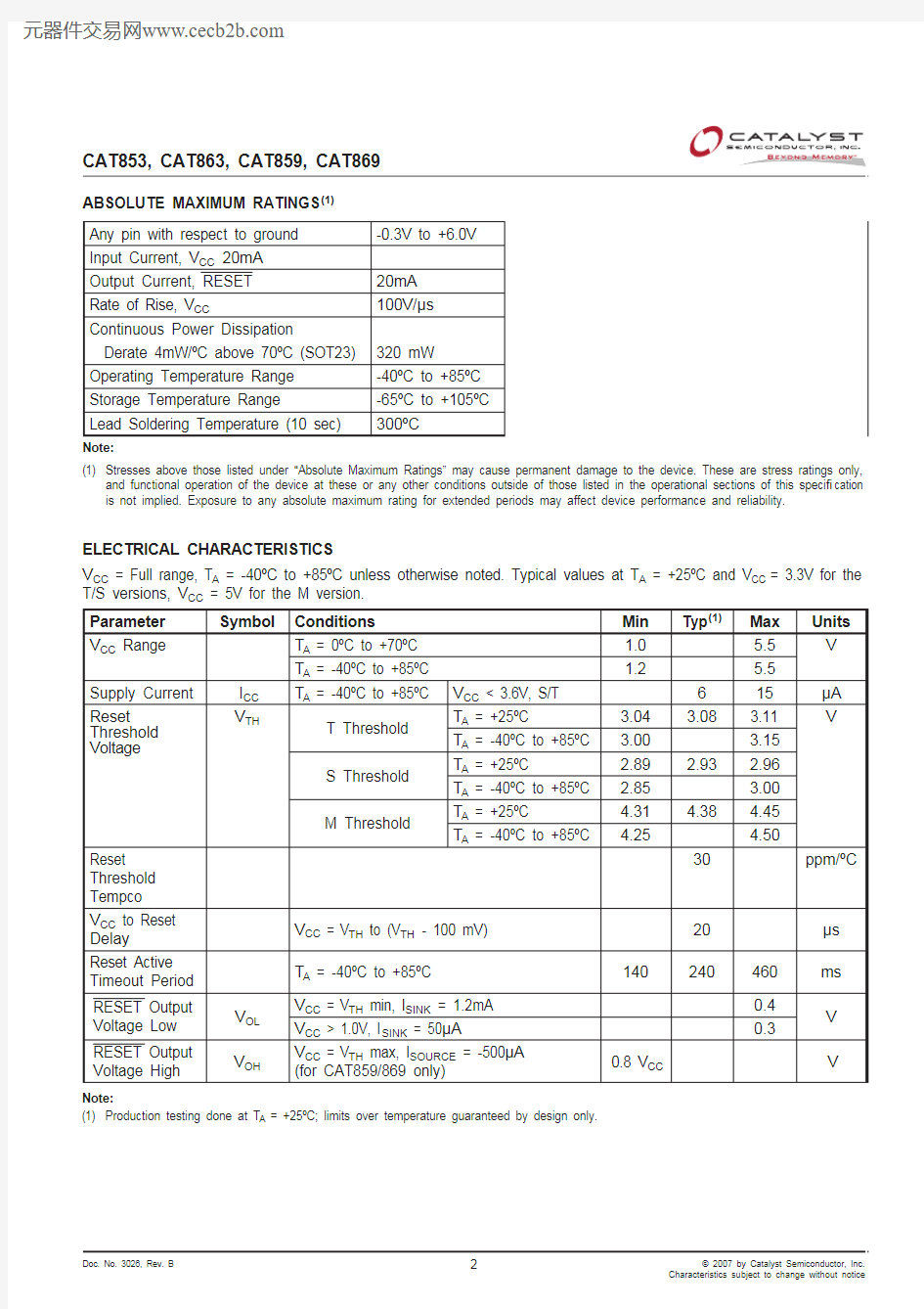
T YPICAL OPERATING CHARACTERISTICS V CC = Full range, T A = -40oC to +85oC unless otherwise noted. Typical values at T A = +25oC, V CC =3.3V for T/S versions, and V CC = 5V for the M version.
SUPPLY CURRENT VS. TEMPERATURE
(NO LOAD)
12
1086420
-50 0 50 100 150
S U P P L Y C U R R E N T (μA )
TEMPERATURE (°C)
POWER-DOWN RESET DELAY
VS. TEMPERATURE
1412108642
P O W E R -D O W N R E S E T D E L A Y (μS )
TEMPERATURE (°C)POWER-UP RESET TIMEOUT
VS. TEMPERATURE
260
240220200
180160
P O W E R -U P R E S E T T I M E O U T (m S )
TEMPERATURE (°C)NORMALIZED RESET THRESHOLD
VS. TEMPERATURE
1.0002
10.99980.99960.99940.99920.9990.9988
0 20 40 60 80 100 120
N O R M A L I Z E D T H R E S H O L D
TEMPERATURE (°C)
-50 0 50 100 150
-50 0 50 100 150
4
Doc. No. 3026, Rev. B? 2007 by Catalyst Semiconductor, Inc.
Characteristics subject to change without notice
CAT853, CAT863, CAT859, CAT869
5
Doc No. 3026, Rev. B
? 2007 by Catalyst Semiconductor, Inc.
Characteristics subject to change without notice
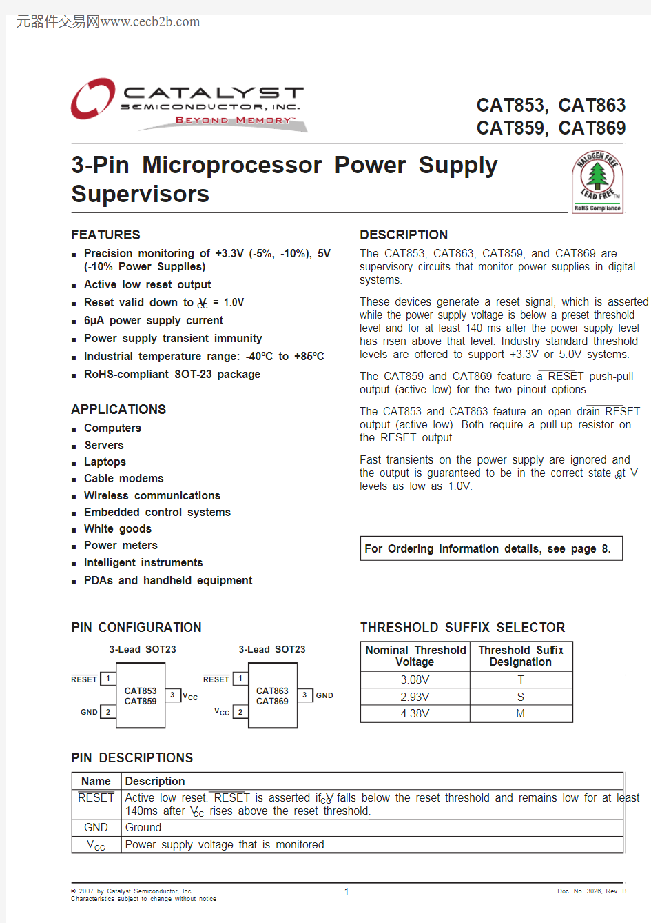
V ALID RESET WITH V CC UNDER 1.0V To ensure that the CAT859 and CAT869 RESET pin is in a known state when V CC is under 1.0V, a >10k Ω pull-down resistor between RESET pin and GND is recommended.
Power Supply
CC Under 1.0V
Figure 4. Bi-directional Reset Pin Interfacing
Power Supply
B I-DIRECTIONAL RESET PIN INTERFACING The CAT859 and CAT869 can interface with μP/μ
C bi-directional reset pins by connecting a 4.7k Ω resistor in series with the CAT859 and CAT869 reset output and the μP/μC bi-directional reset pin.
6
Doc. No. 3026, Rev. B? 2007 by Catalyst Semiconductor, Inc.
Characteristics subject to change without notice
CAT853, CAT863, CAT859, CAT869
7
Doc No. 3026, Rev. B
? 2007 by Catalyst Semiconductor, Inc.
Characteristics subject to change without notice
P ACKAGE INFORMATION Plastic SOT-23 (3-Pin)
Notes:
(1) This part is compliant with JEDEC speci ? cation TO-236(2) Die is face up for mold and trim/form (3) Dimensions are exclusive of mold ? ash and metal burr
Inches Millimeters Min
Max Min Max Plastic SOT-23 (3-Pin)
A 0.03500.04410.89 1.12A10.00050.00390.0130.10
B 0.01460.01970.370.50c 0.00330.00710.0850.18D 0.11020.1197 2.80 3.04E 0.04720.0551 1.20 1.40e 0.03500.04060.89 1.03e10.07010.0807 1.78 2.05H 0.08270.1039 2.10 2.64?0o8o0o8oL 0.00830.01610.2750.41L1
0.0160
0.0270
0.275
0.685
?
For current Tape and Reel information,
download the PDF ? le from:
https://www.doczj.com/doc/6e9579079.html,/documents/tapeandreel.pdf
8
Doc. No. 3026, Rev. B? 2007 by Catalyst Semiconductor, Inc.
Characteristics subject to change without notice
Catalyst Semiconductor, Inc.Corporate Headquarters 2975 Stender Way Santa Clara, CA 95054Phone: 408.542.1000Fax: https://www.doczj.com/doc/6e9579079.html,
Copyrights, Trademarks and Patents
Trademarks and registered trademarks of Catalyst Semiconductor include each of the following:Beyond Memory?, DPP ?, EZDim?, LDD?, MiniPot? and Quad Mode?
Catalyst Semiconductor has been issued U.S. and foreign patents and has patent applications pending that protect its products.
CATALYST SEMICONDUCTOR MAKES NO WARRANTY, REPRESENTATION OR GUARANTEE, EXPRESS OR IMPLIED, REGARDING THE SUITABILITY OF ITS PRODUCTS FOR ANY PARTICULAR PURPOSE, NOR THAT THE USE OF ITS PRODUCTS WILL NOT INFRINGE ITS INTELLECTUAL PROPERTY RIGHTS OR THE RIGHTS OF THIRD PARTIES WITH RESPECT TO ANY PARTICULAR USE OR APPLICATION AND SPECIFICALLY DISCLAIMS ANY AND ALL LIABILITY ARISING OUT OF ANY SUCH USE OR APPLICATION, INCLUDING BUT NOT LIMITED TO, CONSEQUENTIAL OR INCIDENTAL DAMAGES.
Catalyst Semiconductor products are not designed, intended, or authorized for use as components in systems intended for surgical implant into the body, or other applications intended to support or sustain life, or for any other application in which the failure of the Catalyst Semiconductor product could create a situation where personal injury or death may occur.
Catalyst Semiconductor reserves the right to make changes to or discontinue any product or service described herein without notice. Products with data sheets labeled “Advance Information” or “Preliminary” and other products described herein may not be in production or offered for sale.
Catalyst Semiconductor advises customers to obtain the current version of the relevant product information before placing orders. Circuit diagrams illustrate typical
semiconductor applications and may not be complete.
Document No: 3026Revision: B Issue date: 05/04/07
R EVISION HISTORY Date Rev.Reason
10/11/2006A Initial Issue CAT859, CAT869
05/04/2007
B
Added CAT853, CAT863
Update Example of Ordering Information Update Top Marking
Update Ordering Part Number