IP5109 datasheet v1.0
- 格式:pdf
- 大小:2.61 MB
- 文档页数:13

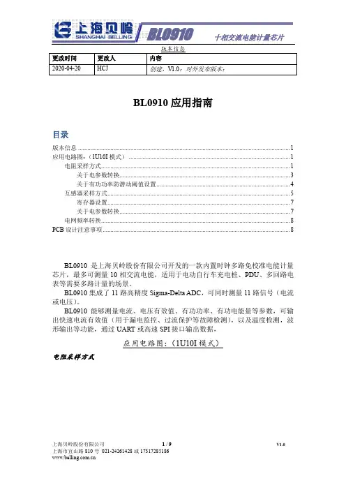
BL0910应用指南目录版本信息 (1)应用电路图:(1U10I模式) (1)电阻采样方式 (1)关于电参数转换 (3)关于有功功率防潜动阈值设置 (4)互感器采样方式 (5)寄存器设置 (7)关于电参数转换 (7)电网频率转换 (8)PCB设计注意事项 (8)BL0910是上海贝岭股份有限公司开发的一款内置时钟多路免校准电能计量芯片,最多可测量10相交流电能,适用于电动自行车充电桩、PDU、多回路电表等需要多路计量的场景。
BL0910集成了11路高精度Sigma-Delta ADC,可同时测量11路信号(电流或电压)。
BL0910能够测量电流、电压有效值、有功功率、有功电能量等参数,可输出快速电流有效值(用于漏电监控、过流保护等故障检测),以及温度检测,波形输出等功能,通过UART或高速SPI接口输出数据,应用电路图:(1U10I模式)电阻采样方式上海贝岭股份有限公司2 / 9V1.0 上海市宜山路810号************或173****5186注意:1)M1~M10缺省功能为过流报警输出,M2管脚可配置为校表脉冲输出(具体配置见MODE3寄存器说明);2)SPI、UART接口的速率,通信协议的描述见“BL0910 datasheet v1.0.pdf”;3)BL0910在出厂时已做增益修正,如果要免校准,外围器件的精度保证在1%以内;4)Uart通信模式时,RX、TX管脚需要外接上拉电阻;寄存器设置采用1毫欧合金电阻进行采样时,电流通道采用16倍增益,电压通道采用1倍增益;0000=1倍;0001=2倍;0010=8倍;0011=16倍;(注意:输入通道的最大差分电压±0.6V指的是1倍增益,如果使用16倍增益,则输入通道的最大差分电压为±37.5mV)注意:需要先向0x9E(US_WRPROT)寄存器写入0x5555后,才能写入增益相关设置!关于电参数转换BL0910在定义产品时考虑到大部分用户厂家不是专业计量器具厂家,没有专业的校准设备,对电能计量精度要求也相对较低,只是提供用电参考信息,不作计费标准。
2.1A Power Switch with Programmable Current LimitGeneral DescriptionThe LPW5209 is an integrated power switch for self-powered and bus-powered Universal Series Bus (USB) applications. A built-in charge pump is used to drive the N-Channel MOSFET that is free of parasitic body diode to eliminate any reversed current flow across the switch when it is powered off. Its low quiescent current (30μA) and small package (SOT23-5) is particularly suitable in battery-powered portable equipment.Several protection functions include soft start to limit inrush current during plug-in, current limiting at 2.1A to meet USB power requirement, and thermal shutdown to protect damage under over current conditions.Order InformationApplications✧Power Switch✧USB Device✧Battery Charger Circuits Features◆80mΩLow R DS(ON), High-side N-MOSFET ◆2100mA Programmable current limit◆ 2.5V to 6V Input Voltage◆Low Quiescent Current:30μA◆Soft Start Function◆Built-In Short-Circuit Protection◆Built-in Thermal Protection◆RoHS Compliant and 100% Lead (Pb)-Free Typical Application CircuitMarking InformationVINFunctional Pin DescriptionPin DescriptionDescriptionLPW5209A LPW5209-21/11/061 1 Output to system pin.2 2 Ground.3 Connect a resistor to GND for setting current limit.Function Block DiagramAbsolute Maximum Ratings Note 1✧Input Voltage to GND ----------------------------------------------------------------------------------------------------- 7V ✧Output Voltage to GND -------------------------------------------------------------------------------------------------- 7V ✧Other pin to GND ---------------------------------------------------------------------------------------------------------- 6V ✧Maximum Junction Temperature --------------------------------------------------------------------------------- 150°C ✧Operating Ambient Temperature Range (T A) -------------------------------------------------------- -40℃ to 85°C ✧Maximum Soldering Temperature (at leads, 10 sec) ------------------------------------------------------- 260°C Note 1. Stresses beyond those listed under “Absolute Maximum Ratings” may cause permanent damage to the device. These are stress ratings only, and functional operation of the device at these or any other conditions beyond those indicated in the operational sections of the specifications is not implied. Exposure to absolute maximum rating conditions for extended periods may affect device reliability.Thermal Information✧Maximum Power Dissipation (SOT23-5, P D, T A=25°C)----------------------------------------------------- 0.45W ✧Thermal Resistance (SOT23-5, θJA) ------------------------------------------------------------------------- 250℃/WESD Susceptibility✧HBM(Human Body Mode) --------------------------------------------------------------------------------------------- 2KV ✧MM(Machine Mode) --------------------------------------------------------------------------------------------------- 200VElectrical Characteristics(Over recommended operating conditions unless specified otherwise, T =25℃)Enable Threshold LowEnable Threshold High 1.4Input High Current V IN=V EN=5.0V 5Typical Operating CharacteristicsApplication InformationThe LPW5209 are single N-Channel MOSFET high-side power switches with active-high enable input, optimized for self-powered and bus-powered Universal Serial Bus (USB) applications. The LPW5209 equipped with a charge pump circuitry to drive the internal NMOS switch; the switch's low RDS(ON), 80mΩ, meets USB voltage drop requirements.Input and OutputVIN (input) is the power source connection to the internal circuitry and the drain of the MOSFET. VOUT (output) is the source of the MOSFET. In a typical application, current flows through the switch from VIN to VOUT toward the load. If VOUT is greater than VIN, current will flow from VOUT to VIN since the MOSFET is bidirectional when on. Unlike a normal MOSFET, there is no a parasitic body diode between drain and source of the MOSFET, the LPW5209 prevents reverse current flow if VOUT being externally forced to a higher voltage than VIN when the output disabled (VEN < 0.4V). Chip Enable InputThe switch will be disabled when the EN pin is in a logic low condition. During this condition, the internal circuit is turned off, reducing the supply current to 0.1μA typical. The maximum guaranteed voltage for a logic low at the EN pin is 0.4V. A minimum guaranteed voltage of 1.4V at the EN pin will turn the LPW5209 back on. Floating the input may cause unpredictable operation. EN should not be allowed to go negative with respect to GND. The EN pin may be directly tied to VIN to keep the part on.Soft Start for Hot Plug-In ApplicationsIn order to eliminate the upstream voltage droop caused by the large inrush current during hot-plug events, the “soft-start” feature effectively isolates the power source from extremely large capacitive loads, satisfying the USB voltage droop requirements.Thermal ShutdownThermal shutdown is employed to protect the device from damage if the die temperature exceeds approximately 150°C. If enabled, the switch automatically restarts when the die temperature falls 20°C. The output will continue to cycle on and off until the device is disabled or the fault is removed.Packaging InformationSOT23-5。