M95640
M95320
64Kbit and 32Kbit Serial SPI Bus EEPROM
With High Speed Clock
FEATURES SUMMARY
s Compatible with SPI Bus Serial Interface Array (Positive Clock SPI Modes)
s Single Supply Voltage:
–4.5 to 5.5V for M95xxx
–2.5 to 5.5V for M95xxx-W
–1.8 to 5.5V for M95xxx-R
s10MHz, 5MHz or 2MHz clock rate (depending
on ordering options)
s5ms or 10ms Write Time (depending on
ordering options)
s Status Register
s Hardware Protection of the Status Register
s BYTE and PAGE WRITE (up to 32 Bytes)
s Self-Timed Programming Cycle
s Adjustable Size Read-Only EEPROM Area
s Enhanced ESD Protection
s More than 100,000 or 1 million Erase/Write
Cycles (depending on ordering options)
s More than 40 Year Data Retention
November 2003
1/39
M95640, M95320
TABLE OF CONTENTS
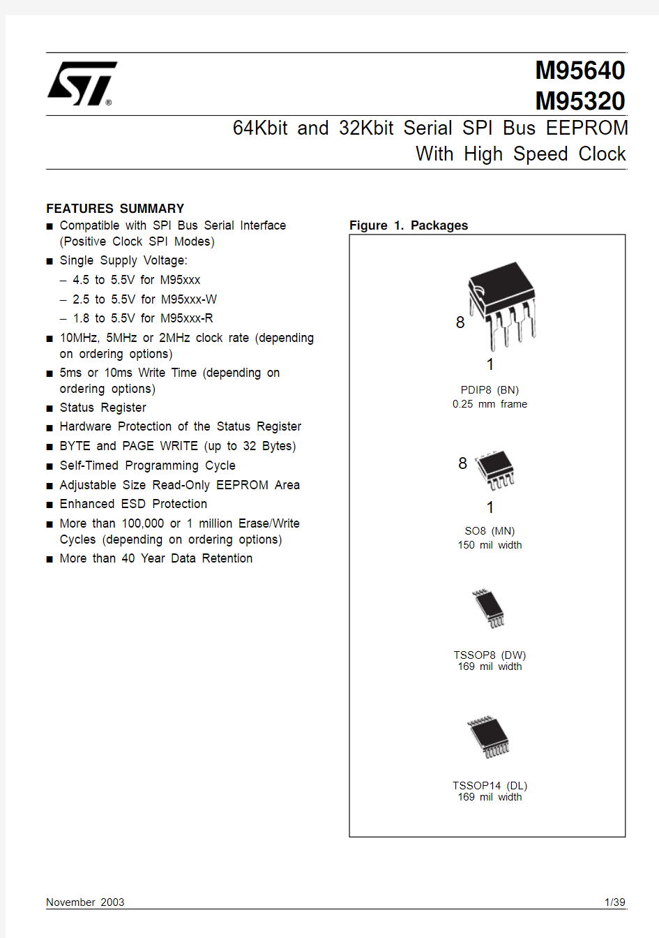
FEATURES SUMMARY . . . . . . . . . . . . . . . . . . . . . . . . . . . . . . . . . . . . . . . . . . . . . . . . . . . . . . . . . . . . .1 Figure 1. Packages . . . . . . . . . . . . . . . . . . . . . . . . . . . . . . . . . . . . . . . . . . . . . . . . . . . . . . . . . . . . . .1
SUMMARY DESCRIPTION. . . . . . . . . . . . . . . . . . . . . . . . . . . . . . . . . . . . . . . . . . . . . . . . . . . . . . . . . . .5
Figure 2. Logic Diagram . . . . . . . . . . . . . . . . . . . . . . . . . . . . . . . . . . . . . . . . . . . . . . . . . . . . . . . . . .5 Figure 3. DIP and SO Connections. . . . . . . . . . . . . . . . . . . . . . . . . . . . . . . . . . . . . . . . . . . . . . . . . .5 Figure 4. TSSOP14 Connections . . . . . . . . . . . . . . . . . . . . . . . . . . . . . . . . . . . . . . . . . . . . . . . . . . .5 Table 1. Signal Names . . . . . . . . . . . . . . . . . . . . . . . . . . . . . . . . . . . . . . . . . . . . . . . . . . . . . . . . . . .5
SIGNAL DESCRIPTION . . . . . . . . . . . . . . . . . . . . . . . . . . . . . . . . . . . . . . . . . . . . . . . . . . . . . . . . . . . . .6
Serial Data Output (Q). . . . . . . . . . . . . . . . . . . . . . . . . . . . . . . . . . . . . . . . . . . . . . . . . . . . . . . . . . . .6 Serial Data Input (D) . . . . . . . . . . . . . . . . . . . . . . . . . . . . . . . . . . . . . . . . . . . . . . . . . . . . . . . . . . . . .6 Serial Clock (C). . . . . . . . . . . . . . . . . . . . . . . . . . . . . . . . . . . . . . . . . . . . . . . . . . . . . . . . . . . . . . . . .6 Chip Select (S) . . . . . . . . . . . . . . . . . . . . . . . . . . . . . . . . . . . . . . . . . . . . . . . . . . . . . . . . . . . . . . . . .6 Hold (HOLD) . . . . . . . . . . . . . . . . . . . . . . . . . . . . . . . . . . . . . . . . . . . . . . . . . . . . . . . . . . . . . . . . . . .6 Write Protect (W). . . . . . . . . . . . . . . . . . . . . . . . . . . . . . . . . . . . . . . . . . . . . . . . . . . . . . . . . . . . . . . .6
CONNECTING TO THE SPI BUS. . . . . . . . . . . . . . . . . . . . . . . . . . . . . . . . . . . . . . . . . . . . . . . . . . . . . .7 Figure 5. Bus Master and Memory Devices on the SPI Bus. . . . . . . . . . . . . . . . . . . . . . . . . . . . . . .7
SPI Modes . . . . . . . . . . . . . . . . . . . . . . . . . . . . . . . . . . . . . . . . . . . . . . . . . . . . . . . . . . . . . . . . . . . .7 Figure 6. SPI Modes Supported . . . . . . . . . . . . . . . . . . . . . . . . . . . . . . . . . . . . . . . . . . . . . . . . . . . .8
OPERATING FEATURES. . . . . . . . . . . . . . . . . . . . . . . . . . . . . . . . . . . . . . . . . . . . . . . . . . . . . . . . . . . .9 Power-up . . . . . . . . . . . . . . . . . . . . . . . . . . . . . . . . . . . . . . . . . . . . . . . . . . . . . . . . . . . . . . . . . . . . .9 Power On Reset: VCC Lock-Out Write Protect. . . . . . . . . . . . . . . . . . . . . . . . . . . . . . . . . . . . . . .9 Power-down. . . . . . . . . . . . . . . . . . . . . . . . . . . . . . . . . . . . . . . . . . . . . . . . . . . . . . . . . . . . . . . . . . .9 Active Power and Stand-by Power Modes . . . . . . . . . . . . . . . . . . . . . . . . . . . . . . . . . . . . . . . . . .9
Hold Condition. . . . . . . . . . . . . . . . . . . . . . . . . . . . . . . . . . . . . . . . . . . . . . . . . . . . . . . . . . . . . . . . .9 Figure 7. Hold Condition Activation. . . . . . . . . . . . . . . . . . . . . . . . . . . . . . . . . . . . . . . . . . . . . . . . . .9
Status Register . . . . . . . . . . . . . . . . . . . . . . . . . . . . . . . . . . . . . . . . . . . . . . . . . . . . . . . . . . . . . . .10 WIP bit. . . . . . . . . . . . . . . . . . . . . . . . . . . . . . . . . . . . . . . . . . . . . . . . . . . . . . . . . . . . . . . . . . . . . . .10 WEL bit . . . . . . . . . . . . . . . . . . . . . . . . . . . . . . . . . . . . . . . . . . . . . . . . . . . . . . . . . . . . . . . . . . . . . .10 BP1, BP0 bits . . . . . . . . . . . . . . . . . . . . . . . . . . . . . . . . . . . . . . . . . . . . . . . . . . . . . . . . . . . . . . . . .10 SRWD bit. . . . . . . . . . . . . . . . . . . . . . . . . . . . . . . . . . . . . . . . . . . . . . . . . . . . . . . . . . . . . . . . . . . . .10 Table 2. Status Register Format . . . . . . . . . . . . . . . . . . . . . . . . . . . . . . . . . . . . . . . . . . . . . . . . . . .10
Data Protection and Protocol Control. . . . . . . . . . . . . . . . . . . . . . . . . . . . . . . . . . . . . . . . . . . . .10 Table 3. Write-Protected Block Size . . . . . . . . . . . . . . . . . . . . . . . . . . . . . . . . . . . . . . . . . . . . . . . .10
MEMORY ORGANIZATION . . . . . . . . . . . . . . . . . . . . . . . . . . . . . . . . . . . . . . . . . . . . . . . . . . . . . . . . .11 Figure 8. Block Diagram . . . . . . . . . . . . . . . . . . . . . . . . . . . . . . . . . . . . . . . . . . . . . . . . . . . . . . . . .11
2/39
M95640, M95320
INSTRUCTIONS . . . . . . . . . . . . . . . . . . . . . . . . . . . . . . . . . . . . . . . . . . . . . . . . . . . . . . . . . . . . . . . . . .12
Table 4. Instruction Set . . . . . . . . . . . . . . . . . . . . . . . . . . . . . . . . . . . . . . . . . . . . . . . . . . . . . . . . . .12 Figure 9. Write Enable (WREN) Sequence. . . . . . . . . . . . . . . . . . . . . . . . . . . . . . . . . . . . . . . . . . .12
Write Enable (WREN) . . . . . . . . . . . . . . . . . . . . . . . . . . . . . . . . . . . . . . . . . . . . . . . . . . . . . . . . . .12 Figure 10. Write Disable (WRDI) Sequence . . . . . . . . . . . . . . . . . . . . . . . . . . . . . . . . . . . . . . . . . .13
Write Disable (WRDI). . . . . . . . . . . . . . . . . . . . . . . . . . . . . . . . . . . . . . . . . . . . . . . . . . . . . . . . . . .13 Figure 11. Read Status Register (RDSR) Sequence . . . . . . . . . . . . . . . . . . . . . . . . . . . . . . . . . . .14
Read Status Register (RDSR). . . . . . . . . . . . . . . . . . . . . . . . . . . . . . . . . . . . . . . . . . . . . . . . . . . .14 WIP bit. . . . . . . . . . . . . . . . . . . . . . . . . . . . . . . . . . . . . . . . . . . . . . . . . . . . . . . . . . . . . . . . . . . . . . .14 WEL bit . . . . . . . . . . . . . . . . . . . . . . . . . . . . . . . . . . . . . . . . . . . . . . . . . . . . . . . . . . . . . . . . . . . . . .14 BP1, BP0 bits . . . . . . . . . . . . . . . . . . . . . . . . . . . . . . . . . . . . . . . . . . . . . . . . . . . . . . . . . . . . . . . . .14 SRWD bit. . . . . . . . . . . . . . . . . . . . . . . . . . . . . . . . . . . . . . . . . . . . . . . . . . . . . . . . . . . . . . . . . . . . .14 Figure 12. Write Status Register (WRSR) Sequence . . . . . . . . . . . . . . . . . . . . . . . . . . . . . . . . . . .15
Write Status Register (WRSR) . . . . . . . . . . . . . . . . . . . . . . . . . . . . . . . . . . . . . . . . . . . . . . . . . . .15 Table 5. Protection Modes. . . . . . . . . . . . . . . . . . . . . . . . . . . . . . . . . . . . . . . . . . . . . . . . . . . . . . . .16 Table 6. Address Range Bits. . . . . . . . . . . . . . . . . . . . . . . . . . . . . . . . . . . . . . . . . . . . . . . . . . . . . .16 Figure 13. Read from Memory Array (READ) Sequence . . . . . . . . . . . . . . . . . . . . . . . . . . . . . . . .17
Read from Memory Array (READ) . . . . . . . . . . . . . . . . . . . . . . . . . . . . . . . . . . . . . . . . . . . . . . . .17 Figure 14. Byte Write (WRITE) Sequence. . . . . . . . . . . . . . . . . . . . . . . . . . . . . . . . . . . . . . . . . . . .18
Write to Memory Array (WRITE). . . . . . . . . . . . . . . . . . . . . . . . . . . . . . . . . . . . . . . . . . . . . . . . . .18 Figure 15. Page Write (WRITE) Sequence. . . . . . . . . . . . . . . . . . . . . . . . . . . . . . . . . . . . . . . . . . .19
POWER-UP AND DELIVERY STATE. . . . . . . . . . . . . . . . . . . . . . . . . . . . . . . . . . . . . . . . . . . . . . . . . .20 Power-up State . . . . . . . . . . . . . . . . . . . . . . . . . . . . . . . . . . . . . . . . . . . . . . . . . . . . . . . . . . . . . . .20 INITIAL DELIVERY STATE. . . . . . . . . . . . . . . . . . . . . . . . . . . . . . . . . . . . . . . . . . . . . . . . . . . . . . . . . .20 MAXIMUM RATING. . . . . . . . . . . . . . . . . . . . . . . . . . . . . . . . . . . . . . . . . . . . . . . . . . . . . . . . . . . . . . . .21 Table 7. Absolute Maximum Ratings. . . . . . . . . . . . . . . . . . . . . . . . . . . . . . . . . . . . . . . . . . . . . . . .21 DC and AC PARAMETERS . . . . . . . . . . . . . . . . . . . . . . . . . . . . . . . . . . . . . . . . . . . . . . . . . . . . . . . . .22
Table 8. Operating Conditions (M95xxx). . . . . . . . . . . . . . . . . . . . . . . . . . . . . . . . . . . . . . . . . . . . .22 Table 9. Operating Conditions (M95xxx-W) . . . . . . . . . . . . . . . . . . . . . . . . . . . . . . . . . . . . . . . . . .22 Table 10. Operating Conditions (M95xxx-R). . . . . . . . . . . . . . . . . . . . . . . . . . . . . . . . . . . . . . . . . .22 Table 11. AC Measurement Conditions. . . . . . . . . . . . . . . . . . . . . . . . . . . . . . . . . . . . . . . . . . . . . .22 Figure 16. AC Measurement I/O Waveform . . . . . . . . . . . . . . . . . . . . . . . . . . . . . . . . . . . . . . . . . .22 Table 12. Capacitance. . . . . . . . . . . . . . . . . . . . . . . . . . . . . . . . . . . . . . . . . . . . . . . . . . . . . . . . . . .23 Table 13. DC Characteristics (M95xxx, temperature range 6) . . . . . . . . . . . . . . . . . . . . . . . . . . . .23 Table 14. DC Characteristics (M95xxx, temperature range 3) . . . . . . . . . . . . . . . . . . . . . . . . . . . .24 Table 15. DC Characteristics (M95xxx-W, temperature range 6) . . . . . . . . . . . . . . . . . . . . . . . . . .24 Table 16. DC Characteristics (M95xxx-W, temperature range 3) . . . . . . . . . . . . . . . . . . . . . . . . . .25 Table 17. DC Characteristics (M95xxx-R). . . . . . . . . . . . . . . . . . . . . . . . . . . . . . . . . . . . . . . . . . . .25 Table 18. AC Characteristics (M95xxx, temperature range 6) . . . . . . . . . . . . . . . . . . . . . . . . . . . .26
3/39
M95640, M95320
4/39Table 19. AC Characteristics (M95xxx, temperature range 3) . . . . . . . . . . . . . . . . . . . . . . . . . . . .27 Table 20. AC Characteristics (M95xxx-W, temperature range 6) . . . . . . . . . . . . . . . . . . . . . . . . . .28 Table 21. AC Characteristics (M95xxx-W, temperature range 3) . . . . . . . . . . . . . . . . . . . . . . . . . .29 Table 22. AC Characteristics (M95xxx-R). . . . . . . . . . . . . . . . . . . . . . . . . . . . . . . . . . . . . . . . . . . .30 Figure 17. Serial Input Timing. . . . . . . . . . . . . . . . . . . . . . . . . . . . . . . . . . . . . . . . . . . . . . . . . . . . .31 Figure 18. Hold Timing . . . . . . . . . . . . . . . . . . . . . . . . . . . . . . . . . . . . . . . . . . . . . . . . . . . . . . . . . .31 Figure 19. Output Timing. . . . . . . . . . . . . . . . . . . . . . . . . . . . . . . . . . . . . . . . . . . . . . . . . . . . . . . . .32
PACKAGE MECHANICAL . . . . . . . . . . . . . . . . . . . . . . . . . . . . . . . . . . . . . . . . . . . . . . . . . . . . . . . . . .33
Figure 20. PDIP8 – 8 pin Plastic DIP, 0.25mm lead frame, Package Outline. . . . . . . . . . . . . . . . .33 Table 23. PDIP8 – 8 pin Plastic DIP, 0.25mm lead frame, Package Mechanical Data. . . . . . . . . .33 Figure 21. SO8 narrow – 8 lead Plastic Small Outline, 150 mils body width, Package Outline. . . .34 Table 24. SO8 narrow – 8 lead Plastic Small Outline, 150 mils body width, Package Mechanical Data 34
Figure 22. TSSOP8 – 8 lead Thin Shrink Small Outline, Package Outline. . . . . . . . . . . . . . . . . . .35 Table 25. TSSOP8 – 8 lead Thin Shrink Small Outline, Package Mechanical Data. . . . . . . . . . . .35 Figure 23. TSSOP14 - 14 lead Thin Shrink Small Outline, Package Outline . . . . . . . . . . . . . . . . .36 Table 26. TSSOP14 - 14 lead Thin Shrink Small Outline, Package Mechanical Data . . . . . . . . . .36
PART NUMBERING . . . . . . . . . . . . . . . . . . . . . . . . . . . . . . . . . . . . . . . . . . . . . . . . . . . . . . . . . . . . . . .37
Table 27. Ordering Information Scheme. . . . . . . . . . . . . . . . . . . . . . . . . . . . . . . . . . . . . . . . . . . . .37 Table 28. How to Identify Current and Forthcoming Products by the Process Identification Letter37
REVISION HISTORY. . . . . . . . . . . . . . . . . . . . . . . . . . . . . . . . . . . . . . . . . . . . . . . . . . . . . . . . . . . . . . .38 Table 29. Document Revision History. . . . . . . . . . . . . . . . . . . . . . . . . . . . . . . . . . . . . . . . . . . . . . .38
M95640, M95320
SUMMARY DESCRIPTION
These electrically erasable programmable memo-
ry (EEPROM) devices are accessed by a high speed SPI-compatible bus. The memory array is organized as 8192 x 8 bit (M95640), and 4096 x 8 bit (M95320).
The device is accessed by a simple serial interface that is SPI-compatible. The bus signals are C, D and Q, as shown in Table 1 and Figure 2.
The device is selected when Chip Select (S) is tak-en Low. Communications with the device can be interrupted using Hold (HOLD).
Note: 1.See page 33 (onwards) for package dimensions, and how to identify pin-1.
Note: 1.See page 33 (onwards) for package dimensions, and how to identify pin-1.
2.NC = Not Connected
Table 1. Signal Names
C Serial
Clock
D Serial Data Input
Q Serial Data Output
S Chip Select
W Write
Protect
HOLD Hold
V CC Supply Voltage
V SS Ground
5/39
M95640, M95320
6/39
SIGNAL DESCRIPTION
During all operations, V CC must be held stable and within the specified valid range: V CC (min) to V CC (max).
All of the input and output signals must be held High or Low (according to voltages of V IH , V OH , V IL or V OL , as specified in Tables 13 to 17). These sig-nals are described next.
Serial Data Output (Q).This output signal is used to transfer data serially out of the device.Data is shifted out on the falling edge of Serial Clock (C).
Serial Data Input (D).This input signal is used to transfer data serially into the device. It receives in-structions, addresses, and the data to be written.Values are latched on the rising edge of Serial Clock (C).
Serial Clock (C).This input signal provides the timing of the serial interface. Instructions, address-es, or data present at Serial Data Input (D) are latched on the rising edge of Serial Clock (C). Data on Serial Data Output (Q) changes after the falling edge of Serial Clock (C).
Chip Select (S).When this input signal is High,the device is deselected and Serial Data Output
(Q) is at high impedance. Unless an internal Write cycle is in progress, the device will be in the Stand-by mode. Driving Chip Select (S) Low enables the device, placing it in the active power mode.
After Power-up, a falling edge on Chip Select (S)is required prior to the start of any instruction. Hold (HOLD).The Hold (HOLD) signal is used to pause any serial communications with the device without deselecting the device.
During the Hold condition, the Serial Data Output (Q) is high impedance, and Serial Data Input (D)and Serial Clock (C) are Don’t Care.
To start the Hold condition, the device must be se-The main purpose of this in-put signal is to freeze the size of the area of mem-ory that is protected against Write instructions (as specified by the values in the BP1 and BP0 bits of the Status Register).
This pin must be driven either High or Low, and must be stable during all write operations.
M95640, M95320 CONNECTING TO THE SPI BUS
These devices are fully compatible with the SPI protocol.
All instructions, addresses and input data bytes are shifted in to the device, most significant bit first. The Serial Data Input (D) is sampled on the first rising edge of the Serial Clock (C) after Chip Select (S) goes Low.
All output data bytes are shifted out of the device, most significant bit first. The Serial Data Output (Q) is latched on the first falling edge of the Serial Clock (C) after the instruction (such as the Read from Memory Array and Read Status Register in-structions) have been clocked into the device. Figure 5 shows three devices, connected to an MCU, on a SPI bus. Only one device is selected at a time, so only one device drives the Serial Data Output (Q) line at a time, all the others being high impedance.
Note: 1.The Write Protect (W) and Hold (HOLD) signals should be driven, High or Low as appropriate.
SPI Modes
These devices can be driven by a microcontroller with its SPI peripheral running in either of the two following modes:
–CPOL=0, CPHA=0
–CPOL=1, CPHA=1
For these two modes, input data is latched in on the rising edge of Serial Clock (C), and output data is available from the falling edge of Serial Clock (C).
The difference between the two modes, as shown in Figure 6, is the clock polarity when the bus mas-ter is in Stand-by mode and not transferring data:– C remains at 0 for (CPOL=0, CPHA=0)
– C remains at 1 for (CPOL=1, CPHA=1)
7/39
M95640, M95320
8/39
M95640, M95320 OPERATING FEATURES
Power-up
When the power supply is turned on, V CC rises from V SS to V CC.
lowed to follow the V CC voltage. It must not be al-lowed to float, but should be connected to V CC via a suitable pull-up resistor.
sensitive as well as level sensitive. After Power-up, the device does not become selected until a falling edge has first been detected on Chip Select (S). This ensures that Chip Select (S) must have been High, prior to going Low to start the first op-eration.
Power On Reset: V CC Lock-Out Write Protect In order to prevent data corruption and inadvertent Write operations during Power-up, a Power On Reset (POR) circuit is included. The internal reset is held active until V CC has reached the POR threshold value, and all operations are disabled –the device will not respond to any command. In the same way, when V CC drops from the operating voltage, below the POR threshold value, all oper-ations are disabled and the device will not respond to any command.
A stable and valid V CC must be applied before ap-plying any logic signal.
Power-down
At Power-down, the device must be deselected. Chip Select (S) should be allowed to follow the voltage applied on V CC.Active Power and Stand-by Power Modes When Chip Select (S) is Low, the device is en-abled, and in the Active Power mode. The device consumes I CC, as specified in Tables 13 to 17. abled. If an Erase/Write cycle is not currently in progress, the device then goes in to the Stand-by Power mode, and the device consumption drops to I CC1.
Hold Condition
rial communications with the device without reset-ting the clocking sequence.
During the Hold condition, the Serial Data Output (Q) is high impedance, and Serial Data Input (D) and Serial Clock (C) are Don’t Care.
To enter the Hold condition, the device must be Normally, the device is kept selected, for the whole duration of the Hold condition. Deselecting the de-vice while it is in the Hold condition, has the effect of resetting the state of the device, and this mech-anism can be used if it is required to reset any pro-cesses that had been in progress.
signal is driven Low at the same time as Serial Clock (C) already being Low (as shown in Figure 7).
signal is driven High at the same time as Serial Clock (C) already being Low.
Figure 7 also shows what happens if the rising and falling edges are not timed to coincide with Serial Clock (C) being Low.
9/39
M95640, M95320
10/39
Status Register
Figure 8 shows the position of the Status Register in the control logic of the device. The Status Reg-ister contains a number of status and control bits that can be read or set (as appropriate) by specific instructions.
WIP bit.The Write In Progress (WIP) bit indicates whether the memory is busy with a Write or Write Status Register cycle.
WEL bit.The Write Enable Latch (WEL) bit indi-cates the status of the internal Write Enable Latch.BP1, BP0 bits.The Block Protect (BP1, BP0) bits are non-volatile. They define the size of the area to be software protected against Write instructions. SRWD bit.The Status Register Write Disable (SRWD) bit is operated in conjunction with the Write Protect (W) signal. The Status Register Write Disable (SRWD) bit and Write Protect (W)signal allow the device to be put in the Hardware Protected mode. In this mode, the non-volatile bits of the Status Register (SRWD, BP1, BP0) become read-only bits.
Table 2. Status Register Format
Data Protection and Protocol Control
Non-volatile memory devices can be used in envi-ronments that are particularly noisy, and within ap-plications that could experience problems if memory bytes are corrupted. Consequently, the device features the following data protection mechanisms:
s
Write and Write Status Register instructions are
checked that they consist of a number of clock pulses that is a multiple of eight, before they are accepted for execution.
s
All instructions that modify data must be
preceded by a Write Enable (WREN) instruction to set the Write Enable Latch (WEL) bit . This bit is returned to its reset state by the following events:–Power-up
–Write Disable (WRDI) instruction completion –Write Status Register (WRSR) instruction completion –Write (WRITE) instruction completion
s
The Block Protect (BP1, BP0) bits allow part of the memory to be configured as read-only. This is the Software Protected Mode (SPM).s
Protect (BP1, BP0) bits to be protected. This is the Hardware Protected Mode (HPM).
For any instruction to be accepted, and executed,Chip Select (S) must be driven High after the rising edge of Serial Clock (C) for the last bit of the in-struction, and before the next rising edge of Serial Clock (C).
Two points need to be noted in the previous sen-tence:
–The ‘last bit of the instruction’ can be the eighth bit of the instruction code, or the eighth bit of a data byte, depending on the instruction (except for Read Status Register (RDSR) and Read (READ) instructions).
–The ‘next rising edge of Serial Clock (C)’ might (or might not) be the next bus transaction for some other device on the SPI bus.
Table 3. Write-Protected Block Size
b7 b0SRWD
0 0 0 BP1 BP0 WEL WIP
Status Register Write Protect
Block Protect Bits Write Enable Latch Bit
Write In Progress Bit
Status Register Bits
Protected Block
Array Addresses Protected BP1 BP0 M95640 M95320
0 0 none
none none 0 1 Upper quarter 1800h - 1FFFh 0C00h - 0FFFh 1 0 Upper half 1000h - 1FFFh 0800h - 0FFFh 1
1
Whole memory
0000h - 1FFFh
0000h - 0FFFh
M95640, M95320
MEMORY ORGANIZATION
The memory is organized as shown in Figure 8.
11/39
M95640, M95320
12/39
INSTRUCTIONS
Each instruction starts with a single-byte code, as summarized in Table 4.
If an invalid instruction is sent (one not contained in Table 4), the device automatically deselects it-self.
Table 4. Instruction Set
Write Enable (WREN)
The Write Enable Latch (WEL) bit must be set pri-or to each WRITE and WRSR instruction. The only way to do this is to send a Write Enable instruction to the device.
As shown in Figure 9, to send this instruction to the device, Chip Select (S) is driven Low, and the bits of the instruction byte are shifted in, on Serial Data Input (D). The device then enters a wait state. It waits for a the device to be deselected, by Chip Instruc tion Description
Instruction Format WREN
Write Enable
0000 0110WRDI Write Disable 0000 0100RDSR Read Status Register 0000 0101WRSR Write Status Register 0000 0001READ
Read from Memory Array
0000 0011WRITE Write to Memory Array
0000 0010
M95640, M95320
Write Disable (WRDI)
One way of resetting the Write Enable Latch (WEL) bit is to send a Write Disable instruction to the device.
As shown in Figure 10, to send this instruction to the device, Chip Select (S) is driven Low, and the bits of the instruction byte are shifted in, on Serial Data Input (D).The device then enters a wait state. It waits for a
ing driven High.
The Write Enable Latch (WEL) bit, in fact, be-comes reset by any of the following events:
–Power-up
–WRDI instruction execution
–WRSR instruction completion
–WRITE instruction completion.
13/39
M95640, M95320
14/39
Read Status Register (RDSR)
The Read Status Register (RDSR) instruction al-lows the Status Register to be read. The Status Register may be read at any time, even while a Write or Write Status Register cycle is in progress.When one of these cycles is in progress, it is rec-ommended to check the Write In Progress (WIP)bit before sending a new instruction to the device.It is also possible to read the Status Register con-tinuously, as shown in Figure 11.
The status and control bits of the Status Register are as follows:
WIP bit.The Write In Progress (WIP) bit indicates whether the memory is busy with a Write or Write Status Register cycle. When set to 1, such a cycle is in progress, when reset to 0 no such cycle is in progress.
WEL bit.The Write Enable Latch (WEL) bit indi-cates the status of the internal Write Enable Latch.When set to 1 the internal Write Enable Latch is set, when set to 0 the internal Write Enable Latch is reset and no Write or Write Status Register in-struction is accepted.
BP1, BP0 bits.The Block Protect (BP1, BP0) bits are non-volatile. They define the size of the area to be software protected against Write instructions.These bits are written with the Write Status Regis-ter (WRSR) instruction. When one or both of the Block Protect (BP1, BP0) bits is set to 1, the rele-vant memory area (as defined in Table 2) be-comes protected against Write (WRITE)instructions. The Block Protect (BP1, BP0) bits can be written provided that the Hardware Protect-ed mode has not been set.
SRWD bit.The Status Register Write Disable (SRWD) bit is operated in conjunction with the Write Protect (W) signal. The Status Register Write Disable (SRWD) bit and Write Protect (W)signal allow the device to be put in the Hardware Protected mode (when the Status Register Write Disable (SRWD) bit is set to 1, and Write Protect (W) is driven Low). In this mode, the non-volatile bits of the Status Register (SRWD, BP1, BP0) be-come read-only bits and the Write Status Register (WRSR) instruction is no longer accepted for exe-cution.
M95640, M95320
Write Status Register (WRSR)
The Write Status Register (WRSR) instruction al-lows new values to be written to the Status Regis-ter. Before it can be accepted, a Write Enable (WREN) instruction must previously have been ex-ecuted. After the Write Enable (WREN) instruction has been decoded and executed, the device sets the Write Enable Latch (WEL).
The Write Status Register (WRSR) instruction is by the instruction code and the data byte on Serial Data Input (D).
The instruction sequence is shown in Figure 12. The Write Status Register (WRSR) instruction has no effect on b6, b5, b4, b1 and b0 of the Status Register. b6, b5 and b4 are always read as 0. Chip Select (S) must be driven High after the rising edge of Serial Clock (C) that latches in the eighth bit of the data byte, and before the next rising edge of Serial Clock (C). Otherwise, the Write Status Register (WRSR) instruction is not executed. As timed Write Status Register cycle (whose duration is t W) is initiated. While the Write Status Register cycle is in progress, the Status Register may still be read to check the value of the Write In Progress (WIP) bit. The Write In Progress (WIP) bit is 1 dur-ing the self-timed Write Status Register cycle, and is 0 when it is completed. When the cycle is com-pleted, the Write Enable Latch (WEL) is reset. The Write Status Register (WRSR) instruction al-lows the user to change the values of the Block Protect (BP1, BP0) bits, to define the size of the area that is to be treated as read-only, as defined in Table 2.
The Write Status Register (WRSR) instruction also allows the user to set or reset the Status Register Write Disable (SRWD) bit in accordance with the Write Protect (W) signal. The Status Register Write Disable (SRWD) bit and Write Protect (W) signal allow the device to be put in the Hardware Protected Mode (HPM). The Write Status Register (WRSR) instruction is not executed once the Hard-ware Protected Mode (HPM) is entered.
The contents of the Status Register Write Disable (SRWD) and Block Protect (BP1, BP0) bits are fro-zen at their current values from just before the start of the execution of Write Status Register (WRSR) instruction. The new, updated, values take effect at the moment of completion of the ex-ecution of Write Status Register (WRSR) instruc-tion.
15/39
M95640, M95320
16/39
Table 5. Protection Modes
Note: 1.As defined by the values in the Block Protect (BP1, BP0) bits of the Status Register, as shown in Table 3.
The protection features of the device are summa-rized in Table 3.
When the Status Register Write Disable (SRWD)bit of the Status Register is 0 (its initial delivery state), it is possible to write to the Status Register provided that the Write Enable Latch (WEL) bit has previously been set by a Write Enable (WREN) in-struction, regardless of the whether Write Protect When the Status Register Write Disable (SRWD)bit of the Status Register is set to 1, two cases need to be considered, depending on the state of –If Write Protect (W) is driven High, it is possible to write to the Status Register provided that the Write Enable Latch (WEL) bit has previously been set by a Write Enable (WREN) instruction.–If Write Protect (W) is driven Low, it is not pos-sible to write to the Status Register even if the Write Enable Latch (WEL) bit has previously been set by a Write Enable (WREN) instruction.(Attempts to write to the Status Register are re-jected, and are not accepted for execution). As a consequence, all the data bytes in the memo-ry area that are software protected (SPM) by the
Block Protect (BP1, BP0) bits of the Status Reg-ister, are also hardware protected against data modification.
Regardless of the order of the two events, the Hardware Protected Mode (HPM) can be entered:–by setting the Status Register Write Disable (SRWD) bit after driving Write Protect (W) Low –or by driving Write Protect (W) Low after setting the Status Register Write Disable (SRWD) bit.The only way to exit the Hardware Protected Mode High.
Hardware Protected Mode (HPM) can never be activated, and only the Software Protected Mode (SPM), using the Block Protect (BP1, BP0) bits of the Status Register, can be used.Table 6. Address Range Bits
Note: 1.b15 to b13 are Don’t Care on the M95640.
b15 to b12 are Don’t Care on the M95320.
W Signal SRWD Bit Mode
Write Protection of the
Status Register
Memory Content
Protected Area 1
Unprotected Area 1
10Software Protected (SPM)Status Register is Writable (if the WREN
instruction has set the WEL bit)The values in the BP1
and BP0 bits can be changed Write Protected
Ready to accept Write instructions
001
1
01Hardware Protected (HPM)Status Register is
Hardware write protected The values in the BP1 and BP0 bits cannot be
changed
Write Protected
Ready to accept Write instructions
Device M95640M95320 Address Bits
A12-A0
A11-A0
M95640, M95320
Note:Depending on the memory size, as shown in Table 6, the most significant address bits are Don’t Care.
Read from Memory Array (READ)
As shown in Figure 13, to send this instruction to bits of the instruction byte and address bytes are then shifted in, on Serial Data Input (D). The ad-dress is loaded into an internal address register, and the byte of data at that address is shifted out, on Serial Data Output (Q).
If Chip Select (S) continues to be driven Low, the internal address register is automatically incre-mented, and the byte of data at the new address is shifted out.When the highest address is reached, the address counter rolls over to zero, allowing the Read cycle to be continued indefinitely. The whole memory can, therefore, be read with a single READ instruc-tion.
The Read cycle is terminated by driving Chip Se-lect (S) High. The rising edge of the Chip Select (S) signal can occur at any time during the cycle. The first byte addressed can be any byte within any page.
The instruction is not accepted, and is not execut-ed, if a Write cycle is currently in progress.
17/39
M95640, M95320
18/39
Note:Depending on the memory size, as shown in Table 6, the most significant address bits are Don’t Care.
Write to Memory Array (WRITE)
As shown in Figure 14, to send this instruction to the device, Chip Select (S) is first driven Low. The bits of the instruction byte, address byte, and at least one data byte are then shifted in, on Serial Data Input (D).
The instruction is terminated by driving Chip Se-lect (S) High at a byte boundary of the input data.In the case of Figure 14, this occurs after the eighth bit of the data byte has been latched in, in-dicating that the instruction is being used to write a single byte. The self-timed Write cycle starts,and continues for a period t WC (as specified in Ta-bles 18 to 22), at the end of which the Write in Progress (WIP) bit is reset to 0.
If, though, Chip Select (S) continues to be driven Low, as shown in Figure 15, the next byte of input data is shifted in, so that more than a single byte,starting from the given address towards the end of the same page, can be written in a single internal Write cycle.
Each time a new data byte is shifted in, the least significant bits of the internal address counter are incremented. If the number of data bytes sent to the device exceeds the page boundary, the inter-nal address counter rolls over to the beginning of the page, and the previous data there are overwrit-ten with the incoming data. (The page size of these devices is 32 bytes).
The instruction is not accepted, and is not execut-ed, under the following conditions:
–if the Write Enable Latch (WEL) bit has not been set to 1 (by executing a Write Enable instruction just before)
–if a Write cycle is already in progress
–if the device has not been deselected, by Chip Select (S) being driven High, at a byte boundary (after the eighth bit, b0, of the last data byte that has been latched in)
–if the addressed page is in the region protected by the Block Protect (BP1 and BP0) bits.
M95640, M95320
19/39
M95640, M95320
20/39
POWER-UP AND DELIVERY STATE Power-up State
After Power-up, the device is in the following state:–Stand-by mode
–deselected (after Power-up, a falling edge is re-tions can be started).–not in the Hold Condition
–the Write Enable Latch (WEL) is reset to 0–Write In Progress (WIP) is reset to 0
the SRWD, BP1 and BP0 bits of the Status Regis-ter are unchanged from the previous power-down (they are non-volatile bits).
INITIAL DELIVERY STATE
The device is delivered with the memory array set at all 1s (FFh). The Status Register Write Disable (SRWD) and Block Protect (BP1 and BP0) bits are initialized to 0.