版次:V0.1 頁次:1 / 23================================================
利豐光電股份有限公司
製品仕樣書
產品名稱:0915A015M
產品料號:01509151101
客戶品名:
客戶料號:990000601
修訂一覽表
項次修訂日期版次頁數修訂內容摘要修訂審核核准
1 2009/06/1
2 V0.1 2
3 暫訂版發行
版次:V0.1 頁次:2 / 23
================================================
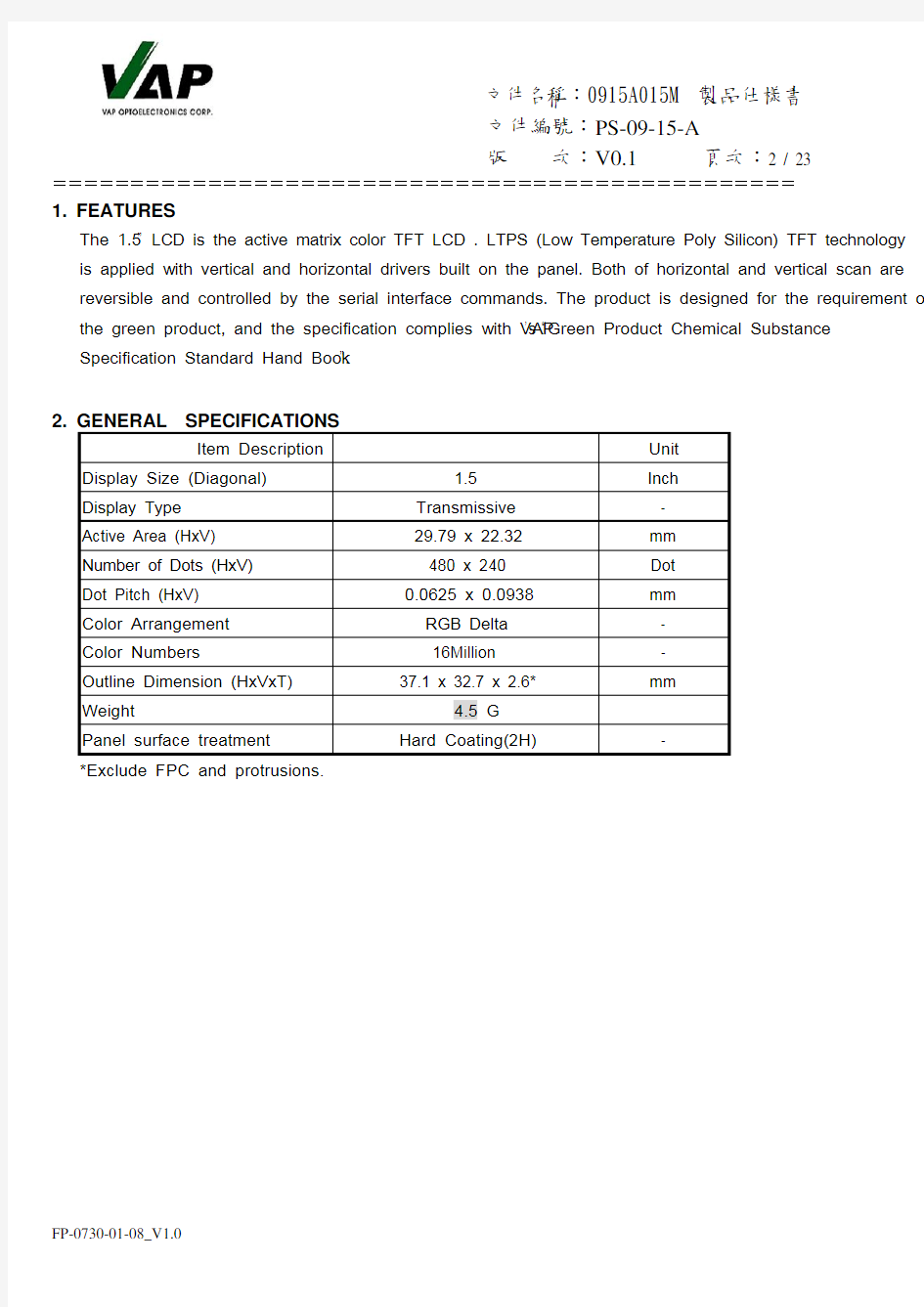
1. FEATURES
The 1.5” LCD is the active matrix color TFT LCD . LTPS (Low Temperature Poly Silicon) TFT technology is applied with vertical and horizontal drivers built on the panel. Both of horizontal and vertical scan are reversible and controlled by the serial interface commands. The product is designed for the requirement of the green product, and the specification complies with VAP’s “Green Product Chemical Substance Specification Standard Hand Book”.
2. GENERAL SPECIFICATIONS
Unit Item Description Display Size (Diagonal) 1.5 Inch
Display Type Transmissive -
Active Area (HxV) 29.79 x 22.32 mm
Number of Dots (HxV) 480 x 240 Dot
Dot Pitch (HxV) 0.0625 x 0.0938 mm
Color Arrangement RGB Delta -
Color Numbers 16Million -
Outline Dimension (HxVxT) 37.1 x 32.7 x 2.6* mm
Weight 4.5 G Panel surface treatment Hard Coating(2H) -
*Exclude FPC and protrusions.
版次:V0.1 頁次:3 / 23================================================3. INPUT/OUTPUT TERMINALS
3.1 TFT LCD Panel
Recommend connector:
Compatible with Molex 51374-4073
Pin Symbol I/O Description Remark
1 CP3 C Capacitor for power setting
2 CP4 C Capacitor for power setting
3 CP5 C Capacitor for charge pump
4 CP6 C Capacitor for charge pump
5 CP7 C Capacitor for charge pump
6 CP8 C Capacitor for charge pump
7 DUMMY -- Dummy
8 DUMMY -- Dummy
9 PCD C Capacitor for pre-charge data signal high
10 VCOML C Capacitor for VCOM low
11 VCOMH C Capacitor for VCOM high
ground
12 AGND -- Analog
13 DUMMY -- Dummy
14 AVDD C Regulation capacitor for analog voltage
15 CP1 C Capacitor for charge pump
16 CP2 C Capacitor for charge pump
17 PWM O Power transistor gate signal for the boost converter
18 FB I Main boost regulator feedback input.
19 LED- LED power: cathode Note 3-1
20 DUMMY -- Dummy
21 DUMMY -- Dummy
22 LED+ LED power: anode Note 3-1
23 GND Ground
24 VCC Power supply
25 VSYNC I Vertical sync input. Negative polarity
26 HSYNC I Horizontal sync input. Negative polarity
27 DCLK I Clock signal, latch data onto line latches at the rising edge
28 DIN0 I Data input
29 DIN1 I Data input
30 DIN2 I Data input
版次:V0.1 頁次:4 / 23================================================
31 DIN3 I Data input
32 DIN4 I Data input
33 DIN5 I Data input
34 DIN6 I Data input
35 DIN7 I Data input
36 SDA I/O Serial interface data line
37 SCL I Serial interface clock line
38 SCEN I Serial interface chip enable line
39 SHDB I Sleep mode setting pin
40 GREST I Grobal reset pin
Note 3-1: The figure below shows the connection of backlight LED.
版次:V0.1 頁次:5 / 23
================================================
4. ABSOLUTE MAXIMUM RATINGS
Ta = 25℃
Item Symbol
MIN
MAX
Unit
Remark Logic Power Supply Voltage V CC -0.5 5 V
Input Signal Voltage V IN1 0 V CC V
VD, HD, DCLK, DIN[0:7], SDA, SCL, SCEN, SHDB, GRESTB
Back Light Forward Current I F-- 27 mA Operating Temperature T OPR 0 +60 ℃
Storage Temperature T STG -30 +80 ℃
版 次:V0.1 頁次:6 / 23
================================================
5. ELECTRICAL CHARACTERISTICS
5.1. Driving TFT LCD Panel
GND=0V, Ta=25℃
Item Symbol MIN TYP MAX Unit Remark
Power Supply Voltage V CC 2.85 3.0 3.6 V Note 5-1
Low Level V IL GND - 0.2x Vcc*V
Input Signal Voltage
High Level
V IH 0.8x Vcc*- Vcc* V VD, HD, DCLK,
DIN[0:7], SDA, SCL,
SCEN, SHDB, GRESTB
PWM Output Voltage V
PWM 0 - Vcc* V Feedback Voltage V FB
0.55
0.6
0.65
V
Note 5-2
Panel Power Consumption W P - - 50 mW
Vcc* =Vcc (TYP)
Note 5-1: The Vcc power is provided for overall panel module supply voltage. Note 5-2: DC/DC feedback control voltage
5.2 Driving Backlight
Ta=25℃
Item Symbol MIN TYP MAX Unit Remark
Forward Current I F - 23 25 mA Forward Current Voltage V F
- 3.4 - V Backlight Power Consumption W BL - 78.2 - mW
Note 5-3
Note 5-3: Backlight driving circuit is recommended as the fix current circuit.
* Ta: Ambient Temperature.
* High temperature operation: Test current refers the diagram as following. * High Temperature & High Humidity Operation: Test current is 15mA.
================================================
6. TIMING CHART
6.1 Through Mode: Horizontal
MAX
Unit
TYP
MIN
Item Symbol
DCLK Frequency DCLK -- 10.36 -- MHz
Horizontal Display Active Display Area-- 480 -- DCLK
Horizontal Total Time t h-- 659 -- DCLK HSYNC Pulse Width t hpw 1 -- DCLK Horizontal Back Porch t hb-- 96 -- DCLK Horizontal Front Porch t hfp -- 83 -- DCLK
版次:V0.1 頁次:8 / 23================================================6.2 Through Mode: Vertical
版 次:V0.1 頁次:9 / 23
================================================
(1) Non-Interlace Mode
(2) Non-Interlace Mode
Item Symbol MIN TYP MAX Unit
Vertical Display Active t vd - 240 - Line Vertical Total Time t v - 262 - Line VSYNC Pulse Width t vpw 1 1 - DCLK Odd Field t vbo - 14 - Line Vertical Back Porch Even Field t vbe - 14 - Line Odd Field t vfpo - 8 - Line Vertical Front Porch
Even Field
t vfpe - 8 - Line Vertical Dummy t vdm
-
-
Line
Item Symbol MIN TYP MAX Unit
Vertical Display Active t vd - 240 - Line Vertical Total Time t v
- 262.5 - Line
VSYNC Pulse Width t vpw 1 1 - DCLK Odd Field t vbo - 14 - Line Vertical Back Porch
Even Field t vbe - 14.5 - Line Odd Field t vfpo - 8.5 - Line Vertical Front
Porch
Even Field
t vfpe - 8 - Line
Vertical Dummy
t vdm - 0 - Line
版 次:V0.1 頁次:10 / 23
================================================
6.3 Serial RGB Dummy Mode and Serial YUV 4:2:2 Mode: Horizontal
(1) YUV Mode: ITUR601-NTSC
(2) YUV Mode: ITUR601-PAL
Item Symbol MIN TYP MAX Unit
Dot Clock Period DCLK -- 27 -- MHz Horizontal Display Active Display Area
--
1440
--
DCLK
Horizontal Total Time t h -- 1716 -- DCLK HSYNC Pulse Width t hpw -- 1 -- DCLK Horizontal Back Porch t hb -- 240 -- DCLK Horizontal Front Porch
t hfp
-- 36 -- DCLK
Item Symbol MIN TYP MAX Unit
Dot Clock Period DCLK -- 27 -- MHz Horizontal Display Active Display Area
--
1440
--
DCLK
Horizontal Total Time t h -- 1728 -- DCLK HSYNC Pulse Width t hpw -- 1 -- DCLK Horizontal Back Porch t hb -- 240 -- DCLK Horizontal Front Porch
t hfp
-- 48 -- DCLK
版 次:V0.1 頁次:11 / 23
================================================
(3) PGB Dummy Mode
Item Symbol MIN TYP MAX Unit
QVGA -- 25 -- NTSC -- 25.54 --
Dot Clock Fre-quency
PAL
DCLK -- 24.38 -- MHz Horizontal Display Active Display Area
--
1280
--
DCLK
Horizontal Total Time t h -- 1560 -- DCLK HSYNC Pulse Width t hpw -- 1 -- DCLK Horizontal Back Porch t hb -- 240 -- DCLK Horizontal Front Porch
t hfp
-- 40 -- DCLK
================================================
6.4 Serial RGB Dummy Mode and Serial YUV 4:2:2 Mode: Vertical
(1) Non-Interlace Mode: NTSC/QVGA
MAX
TYP
Unit Item Symbol
MIN
Vertical Display Active t vd - 240 - Line
Vertical Total Time t v - 262 - Line
VSYNC Pulse Width t vpw 1 1 - DCLK
Vertical
Odd Field t vbo - 21 - Line Back Porch Even Field t vbe - 21 - Line
Vertical Front
Odd Field t vfpo - 1 - Line Porch Even Field t vfpe - 1 - Line
Vertical Dummy t vdm - 0 - Line
版 次:V0.1 頁次:13 / 23
================================================
(2) Non-Interlace Mode: PAL
(3) Interlace Mode: NTSC/QVGA
(4) Interlace Mode: PAL
Item Symbol MIN TYP MAX Unit
Vertical Display Active t vd - 288 - Line Vertical Total Time t v - 312 - Line
VSYNC Pulse Width t vpw 1 1 - DCLK Odd Field t vbo - 24 - Line Vertical Back Porch
Even Field t vbe - 24 - Line Odd Field t vfpo - 0 - Line Vertical Front
Porch
Even Field
t vfpe - 0 - Line
Vertical Dummy
t vdm - 0 - Line
Item Symbol MIN TYP MAX Unit
Vertical Display Active t vd - 240 - Line Vertical Total Time t v
- 262.5 - Line
VSYNC Pulse Width t vpw 1 1 - DCLK Odd Field t vbo - 21 - Line Vertical Back Porch Even Field t vbe - 21.5 - Line Odd Field t vfpo - 1.5 - Line Vertical Front Porch
Even Field
t vfpe - 1 - Line
Vertical Dummy
t vdm - 0 - Line
Item Symbol MIN TYP MAX Unit
Vertical Display Active t vd - 288 - Line Vertical Total Time t v - 312 - Line
VSYNC Pulse Width t vpw 1 1 - DCLK Odd Field t vbo - 24 - Line Vertical Back Porch Even Field t vbe - 24.5 - Line Odd Field t vfpo - 0.5 - Line Vertical Front Porch
Even Field
t vfpe - 0 - Line
Vertical Dummy
t vdm - 0 - Line
版次:V0.1 頁次:14 / 23================================================6.5 Setup Time and Hold Time
Item Symbol MIN TYP MAX Unit DCLK Duty Ratio - 40 - 60 % Data Setup Time t ds 12 - - ns Data Hold Time t dh 12 - - ns Control Signal Setup Time t ss 12 - - ns Control Signal Hold Time t sh 12 - - ns
版次:V0.1 頁次:15 / 23================================================6.6 Serial Interface Timing
Parameter Symbol Condition MIN TYP MAX Unit
t S0 SCEN to SCL 150 - - ns Data Setup Time
t S1 SDA to SCL 150 - - ns
t H0 SCEN to SCL 150 - - ns Data Hold Time
t H1 SDA to SCL 150 - - ns
t W1L SCL pulse width 160 - - ns Pulse width t W1H SCL pulse width 160 - - ns
t W2 SCEN pulse width 1.0 - - us Clock Duty - SCL duty ratio 40 - 60 %
版次:V0.1 頁次:16 / 23================================================
7 POWER SEQUENCE
7.1 Power on to normal mode sequence
Power on (low power mode, global reset) to normal mode sequence
Step1:Wait VCC go stable and then send a low polse(more then 160us) to GRSTB pad.
A normal command is following GRST
B low pulse.
Step2:Before turn on VCC, the VD/HD/DCLK input signal must keep still unit Tpwr(2ms).
Step3:AVDD will start when second VD coming.
Step4:CP_CLK will start when third VD coming.
Step5:Panel Control Signal and Normal DOUT will start when ninth VD coming.
Step6:PWM control signal will start when eleventh VD coming.
版 次:V0.1 頁次:17 / 23
================================================
7.2 Normal mode to power off sequence
8 OPTICAL CHARACTERISTICS
8.1 Optical Specification
Ta=25℃
Item
Symbol
Condition MIN TYP MAX Unit Remarks
Θ11 30 40 -
Θ12 30 40 -
Θ21 10 20 - Viewing Angles
Θ22 CR ≥ 10
40 50 - Degree Note 8-1
Contrast Ratio CR
200
300
-
Note 8-2
Rising
Tr 13 20
Response Time
Falling Tf 22 30
ms Note 8-3
Luminance (I F =
23mA) L 160 200 - cd/m 2 Note 8-4x w - 0.31 -
Chromaticity White y w Θ=0°
- 0.34 -
Note 8-5
8.2 Basic Measure Conditions
(1) Driving voltage
Vcc= 3.3 V
(2) Ambient Temperature: Ta=25℃
(3) Testing Point: Measure in the display center point and the test angle Θ=0° (4) LED Current: I F =23mA. (5) Testing Facility
Environmental illumination: ≤ 1 Lux
版 次:V0.1 頁次:18 / 23
================================================
TFT LCD Module
Note 8-1: Viewing angle diagrams:
Note 8-2: Contrast Ratio:
Contrast ratio is measured in optimum common electrode voltage.
Luminance with white image
CR =
Luminance with black image
Normal θ = 0°
版 次:V0.1 頁次:19 / 23
================================================
Note 8-3: Definition of response time:
100%90%
10%0%
L u m i n a n c e
Note 8-4: Luminance:
Test Point: Display Center
Note 8-5: Chromaticity: The same test condition as Note 8-4.
版次:V0.1 頁次:20 / 23
================================================
9 REILIABILITY
No Test
Item Condition
1 High Temperature Operation Ta=+60℃, 240hrs
2 High Temperature & High Humidity Operation Ta=+40℃, 95% RH, 240hrs
3 Low Temperature Operation Ta=-10℃, 240hrs
4 High Temperature Storage (non-operation) Ta=+80℃, 240hrs
5 Low Temperature Storage (non-operation) Ta=-30℃, 240hrs
6 Thermal Shock (non-operation) -30℃←→80℃, 50 cycles 30 min 30 min
7 Surface Discharge (non-operation) C=150pF, R=330?; Discharge: Air: ±15kV; Contact: ±8kV 5 times / Point; 5 Points / Panel
8 Vibration
(non-operation) Frequency: 10~55Hz; Amplitude: 1.5mm Sweep Time: 11min Test Time: 2 hrs for each direction of X, Y, Z
9 Shock
(non-operation) Acceleration: 100G; Period: 6ms Directions: ±X, ±Y, ±Z; Cycles: Twice
*Ta: Ambient Temperature