mbtutorial
- 格式:pdf
- 大小:1.60 MB
- 文档页数:36

MATLAB培训教程一、引言MATLAB(矩阵实验室)是一种高性能的数值计算和科学计算软件,广泛应用于工程计算、控制设计、信号处理和通信、图像处理、信号检测、财务建模和分析等领域。
MATLAB具有强大的矩阵运算能力、丰富的工具箱和简单易学的编程语言,是科研和工程领域不可或缺的工具。
本教程旨在帮助初学者快速掌握MATLAB的基本使用方法,为后续深入研究打下基础。
二、MATLAB安装与启动1.安装MATLAB从MATLAB官方网站适合您操作系统的MATLAB安装包。
双击安装包,按照提示完成安装。
安装过程中,您可以根据需要选择安装路径、组件和工具箱。
2.启动MATLAB安装完成后,双击桌面上的MATLAB图标或从开始菜单中找到MATLAB并启动。
启动后,您将看到一个包含命令窗口、工作空间、命令历史和当前文件夹等区域的界面。
三、MATLAB基本操作1.命令窗口>>a=3;>>b=4;>>c=a+b;执行后,变量c的值为7。
2.工作空间工作空间用于存储当前MATLAB会话中的所有变量。
您可以在工作空间中查看、编辑和删除变量。
在工作空间窗口中,右键变量名,选择“Open”以查看变量内容。
3.命令历史命令历史记录了您在命令窗口中输入的所有命令。
您可以通过命令历史窗口查看、编辑和重新执行之前的命令。
4.当前文件夹当前文件夹是MATLAB的工作目录,用于存储和访问MATLAB文件。
您可以通过当前文件夹窗口浏览文件系统,打开、创建和保存MATLAB文件。
四、MATLAB编程基础1.变量与数据类型MATLAB中的变量无需声明类型,系统会根据赋值自动确定。
MATLAB支持多种数据类型,如整数、浮点数、字符、字符串、逻辑等。
2.数组与矩阵MATLAB中的数组分为一维数组和多维数组。
多维数组即为矩阵。
在MATLAB中,矩阵的创建和运算非常简单。
例如,创建一个3x3的单位矩阵:>>A=eye(3);3.流程控制语句MATLAB支持常见的流程控制语句,如if-else、for、while 等。

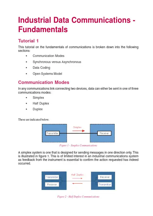
Industrial Data Communications -FundamentalsTutorial 1This tutorial on the fundamentals of communications is broken down into the following sections:M Communication ModesM Synchronous versus AsynchronousM Data CodingM Open Systems ModelCommunication ModesIn any communications link connecting two devices, data can either be sent in one of three communications modes:M SimplexM Half DuplexM DuplexThese are indicated below.Figure 1 - Simplex CommunicationsA simplex system is one that is designed for sending messages in one direction only. This is illustrated in figure 1. This is of limited interest in an industrial communications system as feedback from the instrument is essential to confirm the action requested has indeed occurred.Figure 2 - Half Duplex CommunicationsHalf duplex communications occurs when data flows in both directions; although in only one direction at a time. Half duplex communications (as discussed later) is provided by the RS-485 physical standard (to be discussed later) where only one station can transmit at a time. A protocol (which can be thought of as the pattern of bits and bytes) can be half duplex as well – an example here is ModbusFigure 3 - Full Duplex CommunicationsIn a full duplex system, the data can flow in both directions simultaneously. Examples of hardware standards supporting full duplex are the physical standard EIA-232E (sometimes referred to as RS-232C).Synchronous versus AsynchronousThere are two approaches possible in transmitting data over a communications link. The asynchronous approach is the more basic one used by EIA-232E which operates at a lower speed. The higher speed Local Area Networks running at 10 Mbit/s operate using the more efficient synchronous communications.An asychronous system is one in which each character or byte is sent within a frame. The receiver does not start detection until it receives the first bit, known as the start bit. The start bit is in the opposite voltage state to the idle voltage and allows the receiver to synchronise to the bits following.An asychronous frame may have the following format:M Start Bit Signals the start of the frameM Data Usually 7 or 8 bits of data, but can be 5 or 6M Parity Bit Optional Error detection bitM Stop bits Usually 1, 1.5 or 2 bits.Figure 5 - Asynchronous Frame FormatA synchronous system uses a string of bits to synchronise the receiver before the data is detected. Synchronous systems detect bits by a change in voltage rather than by reading an absolute value as with asynchronous systems. A typical synchronous system frame format is shown below in figure 6.M Preamble This comprises one or more bytes that allow the receiving unit to synchronise with the frameM SFD The start of frame delimiter signals the beginning of the frameM Destination The address to which the frame is sentM Source The address from which the frame is sentM Length Indicates the number of bytes in the data fieldM Data The actual messageM FCS The Frame Check Sequence is for error detectionFigure 6 - Typical Synchronous System Frame format.Data CodingAn agreed standard code allows the receiver to understand the messages sent by a transmitter. The number of bits in the code determines the maximum number of unique characters or symbols that can be represented. The most common character set in the Western World is the American Standard Code for Information Interchange (or ASCII).Table 1 -ASCII Code TableFor example in the table, ‘D’ = ASCII code in binary 1000100Open Systems ModelIn digital data communications, wiring together of two or more devices is one of the first steps in establishing a network. As well as this hardware requirement, software must also be addressed. The OSI reference Model consists of the following seven layers:Figure 7 - The Layers of the OSI ModelM Layer 1 Physical Layer Electrical and mechanical definition of the systemM Layer 2 Data Link Layer Framing and Error correction format of the dataM Layer 3 Network Layer Optimum routing of messages from one network to anotherM Layer 4 T ransport Layer Channel for transfer of messages of one application process to anotherM Layer 5 Session Layer Organisation and synchronisation of the data exchange M Layer 6 Presentation Layer Data format or representationM Layer 7 Application Layer File T ransfer, message exchangeThe OSI Model can be visualised as a collection of entities, such as software programs situated at each of the seven layers. It provides an overall framework for the vendor in which to package their communications solutions comprising the hardware communications links and the protocols.In the world of instrumentation, this OSI model is often simplified to use only three layers: M Layer 1 Physical LayerM Layer 2 Data Link LayerM Layer 3 Application LayerFigure 8 - OSI and Simplified OSI ModelsThis simplifies the operation of the overall system significantly. Y ou will notice that there is another layer mentioned in the three layer model above entitled User layer. This is not part of the OSI model but is a critical part of the overall system and will be discussed later under Fieldbus systems.Examples of how these layers are applied:M RS-232 and RS-485 are examples of the Physical LayerM The Modbus Protocol is an example of the Data Link LayerM Ethernet comprises the Physical and Data Link LayersM The HART smart instrumentation protocol comprises the Physical, Data Link and Application LayersM Profibus and Foundation Fieldbus comprise the Physical, Data Link and Application Layers.Now click here to go to the short quiz based on this tutorial.。


由yzmylh提供,版权所有……Ansys icemcfd 5.1 tutorial部分内容粗略翻译及理解,水平有限,如有问题或建议请联系liqingliang@,不胜感激。
感谢redhong等众多网友提供的资料和帮助,本人正在学习cfx,希望大家多多交流。
ANSYS ICEMCFD 5.1使用手册1. ANSYS ICEMCFD图形用户界面ANSYS ICEMCFD网格编辑器的标准化图形用户界面,提供了一个完善的划分和编辑数值计算网格的环境。
另外,自从ANSYS ICEM CFD 将相应的CAD模型(同样可以生成和编辑)与网格划分链接起来以后,网格编辑器允许用户在修改CAD模型后快速再生成新的网格。
对于为一个模型生成的网格可以被再次链接到一个新的CAD模型上,节约了重新划分网格的时间。
网格编辑器界面包括三个窗口:ANSYS ICEM CFD 主窗口模型的树状目录ANSYS ICEM CFD 信息窗口1.1:ANSYS ICEM CFD 主窗口除了图形显示区,在它的上部设置了一排按钮提供操作菜单,这些菜单包括:几何,网格,块,网格编辑,输出和post processing工具。
窗口的右上角有一串功能菜单,它们与以上这些菜单的选择无关。
文件:文件菜单提供许多与文件管理相关的功能,如:打开文件、保存文件、合并和输入几何模型、存档工程,这些功能方便了管理ANSYS ICEM CFD工程。
在这个菜单里有用的功能包括:新建工程、打开工程、保存工程、另存为、关闭工程、改变工作地址、几何菜单、网格属性、参数、结果、输入几何模型、输入网、输出几何模型和退出。
带有特殊标记的功能按钮包含有子菜单,可以通过点击看到。
编辑:菜单包括回退、前进、命令行、网格转换小面结构、小面结构转化为网格、结构化模型面。
视图:菜单包括合适窗口、放大、俯视、仰视、左视、右视、前视、后视、等角视、视图控制、保存视图、背景设置、镜像与复制、注释、加标记、清除标记、网格截面剖视。

一些常用光学设计软件及其应用方向介绍-物理-小木虫-学术科研第一站一些常用光学设计软件及其应用方向介绍作者: 小龙人收录日期: 2010-03-30 发布日期: 2008-12-08ProduktbilderArtikelbilderAnwendungsbilderArtikeltexteMontageschablonen3DS DatenIES DatenEulumdat DatenDXF DatenCAD SymboleDIALux Plugin 2010AGI PlugIn 2010DIALux ULD Daten (i-drop)3D Studio MAX (i-drop)Autodesk VIZ 4 (i-drop)一些常用光学设计软件及其应用方向介绍【①】LensVIEW 2003.1-ISO 1CD(世界著名的光学设计数据库) 【②】LensVIEW 2001-ISO 1CD(世界著名的光学设计数据库) Focus.Software产品:Zemax v2003-1-6 with manuals & tutorial(专业光学CAD软件,解密,好用的版本)Zemax 用的中国玻璃库 Zemax使用说明书(总计526页)Focus Floor Covering Software 2.0cOptical Research Associates产品:Code V 9.5(世界上应用的最广泛的光学设计和分析软件)Code V 英文使用手册(总计112MBREAULT产品:ASAP v8.0-ISO 1CD(光学分析设计软件合集完全版,包括用户手册、使用实例,解密完全)ASAP 正版光源库 9CDASAP v8.0中文入门指南ReflectorCAD 1.5(中文汉化,ASAP的配套软件,专门用于车灯灯罩设计)Lighting.Technologies产品:PhotoPIA v2.0(快速且精确的光度分析程序)LAS-CAD GmbH产品:LASCAD 3.02(德国LAS-CAD GmbH所开发之固态激光仿真设计分析软件,它是世界上第一套可分析固态激光中光与热特性的多重物理交互作用效应的软件,LASCAD可用来设计传统的气态(Gas)激光,闪光灯(Flash Lamp)激发式固态激光(SSL)与二极管激发式固态激光(DPSSL-Diode Pumped Solid State Laser)RSoft, Inc产品:BeamPROP.v5.1.9.vs.ullwave.v3.0.9.BandSOLVE.v1.3.4.Dif fractMOD.1.0.1.GratingMOD.v1.1.3BeamPROP.v5.1.9.vs集成光导器件的设计及模拟的软件,用类似CAD的界面进行设计,器件的输出能对不同输入光信号进行模拟Fullwave:对复杂光器件进行时域限差模拟,能得到准确的答案BandSolve:光晶体元件的设计及模拟GraingMOD:能设计任意基于集成光导的光栅和滤波器并能根据输入光普推导出光栅的设计Optiwave产品:OptiFDTD 5.0(时域光子学仿真软件,用来模拟先进的被动元件和非线性光电元件)OptiBPM v6.0(用于设计及解决不同的积体及光纤导波问题,光束传播法,或称为BPM是OptiBPM的核心,而其是一种一步接着一步来模拟光通过任何波导物质的行为,BPM可以允许观察任一点被模拟出的光场分布,而且可以容许同时检查辐射光及被传播的光场) OptiSystem 3.0(光通信系统模拟软件,可以设计、测试,与最佳化几乎任何一种在光网路系统的宽谱中的物理层次光连结)TracePro 3.2.2专家版-ISO 1CD(光学机构仿真软件,普遍用于照明系统、光学分析、辐射分析及光度分析的光线仿真)Agi32.v1.61.50(最新照明设计软件)Apollo.Photonic.Suite.v2.2.WinALL(光子学设计软件,可用于光材料、器件、波导和光路等的设计)DynaLS v2.0(粒子及光谱分析软件)PVSOL N 2.5(光电系统)Rayfront 1.04(灯具设计开发包)Radiant ProMetric v8.1.32(是一款基于Windows的CCD影像光度和色度测量系统)SigView v1.9.0.1(实时光谱分析软件)Glastik.Professional.v1.0.79(玻璃厚度演算的有限元软件)TracePro 3.2.4 Update onlyTracePro 3.0 用户手册扫描书334MB(扫面效果一般) 1CDTracePro source.光源灯泡库Radiant Prometric 8.1.19(光学测量工业工具)Radiant Prometric Imaging v8.0(CCD亮度、颜色测试、测量和制造QC/QA系统软件)Lighttools V4.0(基于三维立体模型的照明和光学设计软件,可用于模拟照明系统)LucidShape v1.2(光学设计仿真分析)LucidShape 中文学习资料OSLO Light 6.2-ISO 1CD(光学软件,带中文说明书)RSoft LinkSIM v3.4a(光学通讯模拟软件包。
ICEM Tutorial Manual2D Pipe Junction1.1准备1.1.1 从ANASYS安装目录里拷贝输入几何文件(geometry.tin),v130/icemcfd/samples/CFD_Tutorial_files/2DPipeJunct。
1.1.2 打开ANSYS ICEM CFD并打开几何(geometry.tin)。
1.2 Blocking Strategy2D管道几何的blocking strategy包括创建一个T形的blocking并将其用于几何。
2D管道几何相当于一个T形。
右边的非阻塞交叉开关(blocking crossbar)仅需要向上弯曲以组装几何。
你可以通过在block的边和几何的曲线间创建一些附件然后将block的点移动到几何的角落上来将T形blocking的材料应用于这个几何。
接下来的步骤将描述这个过程。
图2. 网格及其拓扑第一步:Block the Geometry几何和部分(part)的信息已经定义了。
在这一步里,你将创建最初的block。
1.创建初始block。
a.初始化2D blockingi.在Part区域中输入FLUID。
ii.在Type下拉菜单中选择2D Plannar。
iii.点击Apply。
b.在Blocking下激活Vertices。
c.在Vertices下选择Numbers。
将blocking下面的Vertices前面的方框勾选,右击,在弹出菜单中选择Numbers即可。
图2给出了包裹几何的初始block。
你将使用这个初始block来创建这个模型的拓扑。
图3. 初始block这些曲线现在被分别上色,并不是由不同部分。
这样可以使你区别不同的曲线实体,这对于某些blocking操作时非常必要的。
你可以通过选择/不选Show Composite激活或者不激活上色命令。
2.将初始block分割为次级block。
本案中,你将使用两个垂直分割和一个水平分割将初始block分割。

in mm and pixels. If positioned over a found spot, the spot coordinates and I/!(I) will be given. If positioned over a predicted spot position the hkl indices will be shown.Holding down the "Shift" key while the "Zoom" icon in the image is selected will show the image within the small dotted square zoomed within the solid square.2. Overview of iMosflmStart the program by typing "imosflm". After a brief pause, the following window will appear:The basic operations listed down the left hand side (Images, Indexing, Strategy, Cell Refinement, Integration, History) can be selected by clicking on the appropriate icon, but those that are not appropriate will be greyed-out and cannot be selected.2.1 Drop Down menusClicking on "Session" will result in a drop-down menu that allows you to save the current session or reload a previously saved session (or read/save a site file (see §14.1) or add images):Clicking on "Settings" will allow you to see (and modify) Experiment settings, Processing options and Environment variables. These will be described later.The three small icons below "Session" allow you to start a new session, open a saved session or save the current session. Moving the mouse over these icons will result in display of a tooltip describing the action taken if the icon is clicked.3. Adding images to a sessionTo add images to a session, use the "Add images..." icon:Select the correct directory from the pop-up Add Images window (the default is the directory in which iMosflm was launched). All files with an appropriate extension (which can be selected) will be displayed. Double-clicking on any file will result in all images with the same template being added to the session. The template is the whole part of the filename prefix, except the number field which specifies the image number. An alternative is to single-click on one image filename and then click on Open.To open one or several images only, check the 'Selected images only' box and then use click followed by Shift+click to select a range of images or Control+click to select individual image files as required.Loaded images will be displayed in the Images window with the start & end phi values displayed (as read from the image header).All images with the same template belong to the same "Sector" of data.Multiple sectors can be read into the same session. Each sector can have a different crystal orientation.Note that a "Warning" has appeared. Click anywhere on the “1 Warning” text to get a brief description of the warning. In this case it is because the direct beam coordinates stored in the MAR image plate images are not 'trusted' by MOSFLM and the direct beam coordinates have been set to the physical centre of the image. Click on the green tick on the right hand side to dismiss this warning; click anywhere outside the warning box to collapse the box; double-click the warning text itself and more details, hints and notes may be available from MOSFLM.The direct beam coordinates (read from the image header or set by MOSFLM) and crystal to detector distance are displayed. These values can be edited if they are not correct.Advanced Usage1. The phi values of images can be edited in the Image window. First click on the Image line to highlight it then click with themouse over the phi values to make them editable allowing new values to be given. These new values are propagated for all following images in the same sector. Starting values for the three missetting angles (PHIX, PHIY, PHIZ) may also beentered following the image phi values.2. To delete a sector click on the sector name to select it (it turns blue) then use the right mouse button on the sector to bring upa "delete" button. Move the mouse over the delete button (it turns blue) and click to delete the sector and its images.Individual images can be deleted from the Images pane in the same way.3. If one sector is added and used for indexing, and then a second sector from the same crystal is added, the matrix for thesecond sector will not be defined. To define it, double-click on the matrix name for the first sector, save it to a file, double-click on the matrix name (Unknown) for the new sector and read the matrix file written for the first sector. Alternatively, it is possible to "drag and drop" the matrix from the first sector onto the second sector (drop onto the sector itself, not the Matrix for the second sector).4. Image DisplayWhen images are added to a session, the first image of the sector is displayed in a separate display window.The "Image" drop-down menu allows display of the previous or next image in the series.The "View" drop-down menu allows the image to be displayed in different sizes (related by scale factors of two), based on the image size and the resolution of the monitor.The "Settings" drop-down menu allows the colour of the predictions to be changed (see Indexing §5.2 for the default colours),The line below allows selection of different images, either using right and left arrow or selecting one from the drop-down list of all images in that sector. Alternatively the image number can be typed into the "Go to" entry box. The "Sum" entry box will allow the display of the sum of several images, but this is not yet fully implemented.The image being displayed can also be changed by double-clicking on an image name in the "Images" pane of the main window. This will also re-active the image window if it has been closed."+" and "-" will zoom the image without changing the centre. The "Fit image" icon will restore the image to its original size (right mouse button will have the same effect). The "Contrast" icon will give a histogram of pixel values. Use the mouse to drag the vertical dotted line, to the right to lighten the image, to the left to darken it. Try adjusting the contrast. The "Lattice" entry window can be used when processing images with multiple lattices present, see multiple lattices §5.3)4.1 Display IconsThe eight icons on the left, control the display of the direct beam position, spots found for indexing, bad spots, predicted spots, masked areas, spot-finding search area, resolution limits and display of the active mask for Rigaku detectors respectively.These are followed by icons for Zoom, Pan and Selection tools, and tools for adding spots manually (for indexing), editing masks, circle fitting and erasing spots or masks.Next on this toolbar are the entry boxes for h, k & l and a button to search for this hkl among the predicted spots displayed on the image. The button resembles a warning sign if the given hkl cannot be found, but a green tick if it is found. The final icon relates to processing images with multiple lattices, (see multiple lattices §5.3) and is not described here.4.1.1 Masked areas - circular backstop shadowSelect the masked area icon. A green circle will be displayed showing the default position and size of the backstop shadow.Make sure that the Zoom icon (magnifying glass) is selected and use the left-mouse-button (abbreviated to LMB in following text) to drag out a rectangle around the centre of the image. The inner dotted yellow rectangle will show the part of the image that will actually appear in the zoomed area.Choose the Selection Tool. When placed over the perimeter of the circle, the radius of the circular backstop shadow will be displayed. Use the LMB to drag the circle to increase its diameter to that of the actual shadow on the image. The position of the circle can be adjusted with LMB placed on the cross that appears in the centre of the green circle. Adjust the size and position of the circle so that it matches the shadow.4.1.2 Masked areas - general exclusionsChoose the Masking tool. Any existing masked areas will automatically be displayed. Use LMB to define the four corners of the region to be masked. When the fourth position is given, the masked region will be shaded. This region will be excluded from spot finding and integration. This provides a powerful way of dealing with backstop shadows. To edit an existing mask, choose the Selection tool and use the LMB to drag any of the four vertices to a new position.To delete a mask, choose the Spot and mask eraser tool. Place the mouse anywhere within the shaded masked area, and use LMB to delete the mask. Delete any masks that you have created.4.1.3 Spot search areaSelect the Show spotfinding search area icon. The inner and outer radii for the spot search will be displayed as shown below. If the images are very weak, the spot finding radius will automatically be reduced, but this provides additional control.Either can be changed by dragging with the LMB. Do not change the radii for these images.Advanced UsageThe red rectangle displays the area used to determine an initial estimate of the background of the image. It is important that this does not overlap significant shadows on the image. It can be shifted laterally or changed in orientation (in 90° steps) by dragging with the LMB.4.1.4 Resolution limitsSelect the Show resolution limits icon. The low and high resolution limits will be displayed. The resolution limits can be changed by dragging the perimeter of the circle with LMB (make sure that the Selection Tool has been chosen). The resolution limits will affect Strategy, Cell refinement and Integration, but not spot finding or indexing. The low resolution is not strictly correct (it falls within the backstop shadow) but does not need to be changed because spots within the backstop shadow will be rejected.4.1.5 Zooming and PanningFirst select a region of the image to be zoomed with the Zoom tool.Select the Pan tool and pan the displayed area by holding down LMB and moving the mouse. This is very rapid on a local machine, but may be slow if run on a remote machine over a network.4.1.6 Circle fittingThe circle fitting tool can be used to determine the direct beam position by fitting a circle to a set of points on a powder diffraction ring on the image (typically due to icing) or to fit a circular backstop shadow (although using the masking tool is probably easier).Select the circle fitting tool. Three new icons will appear in the image display area. There are two (faint) ice rings visible on the image at 3.91Å and 3.67Å. Click with LMB on several positions (6-8) on the outer ring (as it is slightly stronger). Then click on the top circular icon.A circle that best fits the selected points (displayed as yellow crosses) will be drawn, and the direct beam position at the centre of this circle will be indicated with a green cross. The direct beam coordinates will be updated to reflect this new position.5. Spot finding, indexing and mosaicity estimationWhen images have been added, the "Indexing" operation becomes accessible (it is no longer greyed-out).Click on Indexing. This will bring up the major Indexing window in place of the Images window.5.1 Spot FindingBy default, two images 90 degrees apart in phi (or as close to 90 as possible) will be selected and a spot search carried out on bothimages (This is controlled by the "Automatically find spots on entering Autoindexing" button in the Spot finding tab of Processing options).Found spots will be displayed as crosses in the Image Display window (red for those above the intensity threshold, yellow for those below). The intensity threshold normally defaults to 20, but will be automatically reduced to 10 or 5 for weak images. The threshold is determined by the last image to be processed.The number of spots found, together with any manual additions or deletions, are also given.Images to be searched for spots can be specified in several ways:1. Simply type in the numbers of the images (e.g. 1, 84 above).2. Use the "Pick first image" icon (single blue circle).3. Use the "Pick two images ~90 apart" icon (two blue circles) . This is the default behaviour.4. Use the "Select images ..." icon (multiple circles). If selected, all images in the sector are displayed in a drop-down list. Clickon a image to select it, then double-click on the search icon (resembling a target) for that image to run the spot search. The image will move to the top of the list (together with other images that have been searched).Images to be used for indexing can be selected from those that have been searched by clicking on the "Use" button. If this box was previously checked, then clicking will remove this image from those to be used for indexing. It can be added again by clicking the "Select images ..." icon and clicking on the "Use" box.5.1.1 Difficult imagesParameters affecting the spot search can be modified by selecting the "Settings" drop-down window and selecting "Processing options". The resulting new window contains six tabs relating to Spot finding, Indexing, Processing, Advanced refinement, Advanced integration and Sort, Scale and Merge.The Spot finding window allows the Search area, Spot discrimination parameters, Spot size parameters, Minimum spot separation and Maximum peak separation within spots (to deal with split spots) to be reset. It also allows the choice between a local background determination (preferred) and a radial background determination. The local background method also uses an improved procedure for recognising closely spaced spots. The only parameters commonly changed are:1. Minimum spot separation. This should be the size (in mm) of an average spot (not a very strong spot). Change to valuesestimated by manual inspection of spots if there are difficulties due to badly split spots. This separation parameter is very important when spots are very close, but usually the program will determine a suitable value.2. Minimum pixels per spot. Default value 6, but this will be reduced automatically if spots are very small (eg in situ screeningand microfocus beam).3. Local background box size. Reducing this from 50 to (say) 20 can reduce the number of "false" spots found near any sharpshadow on the image.For data collected in-house spots can be quite large and rather weak. In such cases the spot finding parameters are automatically changed, but some improvement may still be obtained by the following:1. Reduce the spot finding threshold (default 3.5), e.g. to2.2. Increase the minimum number of pixels per spot (default 30) to 20 or 40.3. Set the minimum spot separation to a sensible value, e.g. 1.5mm5.2 IndexingProviding there are no errors during spot finding, indexing will be carried out automatically after spot finding (This is controlled by the "Automatically index after spot finding" button in the Indexing tab of Processing options). If the image selection or indexing parameters are changed, the "Index" button must be used to carry out the indexing.Autoindexing will be carried out by MOSFLM using spots (above the threshold) from the selected images. The threshold is set by MOSFLM but can be changed using the entry box in the toolbar. The list of solutions, sorted by increasing penalty score, will appear in the lower part of the window. The preferred solution will be highlighted in blue. There will usually be a set of solutions with low penalties (0-20) followed by other solutions with significantly higher penalties. The preferred solution is that with the highest symmetry from the group with low penalty values.Note that all these solutions are really the same P1 solution transformed to the 44 characteristic lattices, with latticesymmetry constraints applied. Therefore, if the P1 solution is wrong, then all the others are wrong as well.For solutions with a penalty less than 50, the refined cell parameters ("ref") will be shown. This can be expanded (click on the + sign) to show the "reg" unrefined but regularised cell (symmetry constraints applied) and the "raw" cell (no symmetry constraints applied).The rms deviation (rmsd) or error in predicted spots positions (!(x,y) in mm) and the rms error in (!(") in degrees) are given for each solution.Usually the penalty will be less than 20 for the correct solution, although it could be higher if there is an error in the direct beam coordinates (or distance/wavelength). The rmsd (error in spot positions) will typically be 0.1-0.2mm for a correct solution, but if the spots are split or very elongated it can be as high as 1mm or higher.The predicted spot positions for the highlighted solution will be shown on the image display with the following default colour codes:Blue:Fully recorded reflectionYellow:Partially recorded reflectionRed:Spatially overlapped reflection... these will NOT be integratedGreen:Reflection width too large (more than 5 degrees)... not integrated.These colours may be adjusted via the "Settings - Prediction colour" item in the Image display window.Providing there are no errors in the indexing, MOSFLM will automatically estimate the mosaic spread (mosaicity) based on the preferred solution.Select other solutions with a higher penalty and see how well the predicted patterns match the diffraction image.The rmsd and visual inspection of the predicted pattern are the best ways of checking if a solution is correct. If the agreement is not good, then the autoindexing has probably failed.5.2.1 If the indexing fails - Direct beam searchThe indexing is very sensitive to errors in the direct beam coordinates. For a correct indexing solution, these should be correct to better than half the minimum spot separation. Check, for example, that the current direct beam position is behind the backstop. If there are any ice rings, these can be used to determine the direct beam position (see Circle fitting §4.1.6 ).If the accuracy of the direct beam coordinates (generally read from the image header) is uncertain, the program can perform a grid search around the input coordinates. The number and the size of the steps can be set from the Indexing tab of the Processing options menu (see Settings - Processing options §2.1) but defaults to two steps of 0.5mm on each side of the input coordinates. The direct beam search is started by clicking on the text "Search beam-centre" in the Indexing pane. While in progress, it can be stopped by clicking on the same place, the text of which is now "Abort beam-centre".The indexing will be carried out for each set of starting coordinates (Beam x and Beam y in the table which appears) and, if a solution is found, the refined beam coordinates (Beam x ref, Beam y ref), the unit cell parameters of the triclinic solution and the rmsd error in spot coordinates and in phi will be listed. The correct solution will generally be the one with the smallest rms error in spot positions (!(x,y)). To make it simpler to identify the correct solution, once the grid search has finished the solutions will be sorted on !(x,y), so the correct solution will be at the top of the list. When sorting the solutions, those which have smaller cell parameters will be listed first, as it is possible to have a small!(x,y) value for an incorrect solution with a much larger unit cell.Note that only the triclinic (P1) solution will be listed. To complete the indexing, double-click on the chosen solution, and the full indexing will carried out for these beam coordinates, with the solutions appearing in the upper window. The results of the direct beam search can be hidden (collapsed) by clicking on the [-] symbol next to "Search beam-centre" and recovered by clicking on [+]5.2.2 If the indexing fails - Other parameters.Errors in other physical parameters (wavelength, crystal to detector distance) can also result in failure. All these parameters should be checked.Several parameters used in autoindexing can also be adjusted using entry fields and buttons that appear in the Indexing toolbar.Weak images1. MOSFLM automatically reduces the I/!(I) threshold for weak images and it may also reduce the resolution to 4# but lowervalues can be tried. It is important not to include spots that are not "real" - a small number of false spots can prevent theindexing from working.2. Try changing parameters for spot finding (see Difficult images §5.1.1)Multiple lattices1. Try increasing the I/!(I) threshold (default 20), for example to 40 or 60, so that only spots from the stronger lattice are selected.This can be done by entering a new value in the leftmost of the circled icons above (and also via the using the Indexing tab of Processing options).All cases1. Include more images in the indexing.2. Select images that show the clearest lunes and/or have the best spot shape.3. In case the crystal orientation has changed, or if you are unsure of the direction of positive rotation in phi, try indexing usingonly one image.4. If the cell parameters are known, reduce the maximum allowed cell edge to the known maximum cell edge. This can sometimeshelp filter incorrect solutions, but use with caution as often this needs to be ~twice the largest cell for successful indexing.5. If the detector distance is uncertain, and the images are high resolution (e.g. 2#), allow the detector distance to refine duringcell refinement. Use with caution.5.3 Indexing multiple lattices simultaneouslyThis is a new feature and is still undergoing development. It is most likely to succeed when the different lattices are clearly separated, at least at higher resolution. If the images shows badly split spots with several components (each arising from a sub-crystal with a slightly different orientation) then indexing may well still be impossible.After spot finding, examine the image to ensure that spots that are close to each other but belong to different lattices have been identified as separate spots, and not treated as a single split spot (in which case the red cross will lie midway between the two spots). Adjusting the minimum spot separation (Settings -> Processing options -> Spot finding) can help in resolving close spots. It may also help to increase the inner radius of the spot search region (see Spot search area §4.1.3) so that low resolution reflections where the spots are not really separated are excluded from the search.The following procedure usually provides the best chance of success:1. Select appropriate images for use in indexing. The separation of the lattices can be clearer on some images than others. Ideally choose several images widely separated in phi.2. Do a normal (single lattice) indexing first. This will usually work, but will give a high positional rmsd because of the presence of more than one lattice. This step is important because it will result in more accurate direct beam coordinates, which are crucial for multi-lattice indexing.3. Select “Index multiple lattices” from the drop-down option next to the “Index” button.The indexing results for different lattices will be presented in different tabs, while the selected solution for each lattice will be shown in the lower "Summary" window. Currently a maximum of 5 lattices can be handled. The figure below shows a case where 3 different lattices were found.4. Judge the success of indexing by examining the lattice type and the cell parameters obtained for the different lattices (the cells should be very similar) and checking that the predictions match the observed spots. The rmsd values for correct lattices should also be significantly smaller than the value obtained in the initial (single lattice) indexing. It may be necessary to manually select a different autoindexing solution for some lattices in order to get consistent results for the different lattices.The "Split" column in the lower pane indicates the angle between the reference lattice (with value "-") and the other lattices. This is only calculated when the lattices have the same lattice type. In this case, the angles between lattice 1 and lattices 2 & 3 are 3.4 and 1.6 degrees.If a lattice is clearly incorrect, it can be deleted by highlighting that lattice (in the lower pane that summarises the results) and using the right mouse button to select “delete”.The predictions for different lattices can be displayed either by highlighting the lattice in the Summary window or by using the lattice selector in the image display pane.In the image display, spots in different lattices that overlap with each other are shown in magenta. Only the summed intensity will be measured for these reflections.The predictions for all lattices can be shown by selecting the “merge lattices” icon in the image display.This can be useful to check if all the lattices have been successfully indexed, because all spots in the image should then be predicted. In the display, predictions from lattice 1,2,3,4,5 are shown in blue, yellow, red, green and magenta with no distinction made between fully and partially recorded reflections or spatial overlaps.5.3.1 Practical TipsBeware of solutions where the lattices only vary in orientation by a small angle (less than 1 degree) as these are often different solutions for the same lattice. The difference in orientation between lattices is given by the “split” column in the Summary window, but this is only calculated if the lattices have the same lattice type. Differences are all relative to one lattice, which will display a split angle as “-“. To calculate the angles relative to a different lattice, open the tab for that lattice, select a different solution to that currently selected and then select the original solution – this will trigger recalculation of the split angles relative to that lattice. Other parameters that can influence the indexing are the ”Maximum deviation from integral hkl” (default 0.2 when indexing multiple lattices, otherwise 0.3) and “Number of vectors to find for indexing” (default 30). These can be changed via the Indexing tab of the “Processing Options” that can be selected from the “Settings” menu item. Values between 0.15 and 0.25 might be helpful for the first parameter and increasing the number of vectors from 30 to 50 can also help. At present there is no defined protocol for changing the default parameter values for particular cases, it has to be done by trial and error.Experience so far has shown that selecting appropriate images and adjusting the maximum cell length used in indexing have the biggest effect. The optimum value for the maximum cell length will normally lie between one and three times the largest cell dimension, but it is worth varying this in steps of between 25 and 50 Å, as the indexing can be very sensitive to this parameter.For a more complete discussion of multiple lattice indexing see: Powell, H.R., Johnson, O. & Leslie, A.G.W. 2013. Autoindexing diffraction images with iMosflm. Acta Cryst. D69, 1195-1203.5.4 Space group selectionNote that the indexing is based solely on information about the unit cell parameters. It will therefore be very difficult (or impossible) to determine the correct Laue group in the presence of pseudosymmetry. For example, a monoclinic space group with $ ~ 90 will appear to be orthorhombic; an orthorhombic space group with very similar a and b cell parameters will appear to be tetragonal. These can only be distinguished when intensities are available (i.e. after integration) by running POINTLESS.In addition, it is not possible to distinguish between Laue Groups 4/m and 4/mmm, 3 and 3/m, 6/m and 6/mmm, m3 and m3m. This will not affect integration of the images, but it will affect the strategy calculation. In the absence of additional information, the lower symmetry should be chosen for the strategy calculation to ensure that a complete dataset is collected.The presence of screw axes also cannot be detected, so there is no basis on which to distinguish P21 from P2 etc. This does not affect。
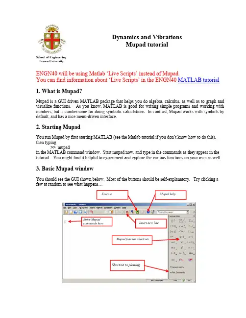
Dynamics and Vibrations Mupad tutorial School of Engineering Brown UniversityENGN40 will be using Matlab ‘Live Scripts’ instead of Mupad. You can find information about ‘Live Scripts’ in the ENGN40 MATLAB tutorial1. What is Mupad? Mupad is a GUI driven MATLAB package that helps you do algebra, calculus, as well as to graph and visualize functions. As you know, MATLAB is good for writing simple programs and working with numbers, but is cumbersome for doing symbolic calculations. In contrast, Mupad works with symbols by default, and has a nice menu-driven interface.2. Starting Mupad You run Mupad by first starting MATLAB (see the Matlab tutorial if you don’t know how to do this), then typing >> mupad in the MATLAB command window. Start mupad now, and type in the commands as they appear in the tutorial. You might find it helpful to experiment and explore the various functions on your own as well.3. Basic Mupad window You should see the GUI shown below. Most of the buttons should be self-explanatory. Try clicking a few at random to see what happens… Mupad function shortcutsEnter Mupad commands here Shortcut to plotting Mupad help Execute Insert new line4. Simple arithmetic calculationsJust like MATLAB itself, Mupad can be used as a calculator. Try the following commandsHere, the gamma function and besselJ are special functions – the gamma function is the generalization of the factorial to non-integers, and the Bessel function is the solution to a common differential equation. Mupad has lots of built in special functions, which can be very useful. Notice also that, unlike MATLAB, Mupad returns the correct answer for sin(PI). This is because by default, Mupad is not working with floating point numbers. It will return the exact answer to any calculation. It will only start using floating point calculations if you start first, or explicitly ask for a numerical value. For example, contrastIn the second case, Mupad gives a floating point number because you typed in a floating point number (0.5) as the argument to the Gamma function. You can also ask Mupad to compute a numerical value for an expression with the ‘float’ functionNote the use of the % character – this always refers to the result of the last calculation that Mupad has done.Note that unlike the MATLAB command window, Mupad lets you go back and change any line, and will then let you execute the file again with the changed code. The Notebook> menu gives lots of options for re-doing calculations after a correction.5. HelpMupad will automatically open the help page for the MATLAB symbolic math toolbox. You can start help by pressing the question mark on the command ribbon or by going to Help, or by pressing the F1 key.Note that the ‘Search Documentation’ box in the help window will search the whole MATLAB help, not just Mupad, so it’s not very useful. But you can find a lot of Mupad examples and information by clicking on the ‘Mupad’ part of help.Try browsing around in the help pages for a bit to get a sense of what is in there.6. Saving your workYou can save your work in a Mupad ‘Notebook’ (a bit like a MATLAB script) by going the the File>Save menu. The file should be saved with the default .mn extension. Mupad is fairly robust, but it does crash unexpectedly now and again (usually when you try to resize a window), so it’s worth saving lengthy calculations frequently.Mupad notebooks can also include detailed comments and annotations that help readers follow what the calculations are doing. To insert a text paragraph, just hit the button, or use Insert>Text Paragraph. Use Insert> Calculation to go back to typing in math, or use the button.You can also export a Mupad notebook to html or pdf format, if you want to publish your work.7. Basic algebraMupad is quite good at doing algebra. For example, it can solve equationsBecause there are two solutions, they are returned in a set (enclosed by {}). You can extract each one by using the [number] convention.IMPORTANT: Notice that the ‘equals’ sign is used in two different ways. If you just type a=b, you have created an equation object that you can use in later manipulations (e.g. solve it!). On the otherhand, if you type a :=b^2 (with a colon) then you have assigned the value b^2 (a symbol) to a variable called a. Mupad will substitute b^2for a any time it is used later. For example try thisNotice that a in the ‘eq1’ object has been replaced by b^2. You can clear the value of a variable using the ‘delete’ functionIf you want to clear all variables, you can use the ‘reset’ function. This completely restarts mupad from the beginning. This is often useful for starting a new homework problem.Let’s try some more algebraMupad doesn’t simplify expressions by default. But it can do so if you ask it toThis sort of thing is especially handy for trigonometric functionsMupad can solve systems of equations tooYou often want to solve an equation or system of equations, and then substitute that solution into a third equation. You can use the ‘subs’ function to do thisAll the [1]s and [2]s here are hard to understand. Their purpose to extract the solutions from the variable ‘sol.’ Notice that ‘sol’ is in curly parentheses {} (look at the example at the top of the page) – this means sol contains a set (which happens to contain only a single solution – but in more complicated problems there might be more than one solution). You need to extract the solution you want out of this set. Thus, sol[1] extracts the first (and only) element from the set. In the first example, both the solutions for x and y are extracted and substituted into eq3. In the second example, sol[1][1] substitutes only x. In the third, sol[1][2] substitutes only y.Of course not all equations can be solved exactly.But you can get an approximate, numerical solutionYou can find more information about equation solving in the Mupad help documentation…8. PlottingMupad is very good at plotting and graphics. For a basic plot, tryYou can control the range of the plot as followsThe ‘plotfunc2d’ command does the same thing as plot but has more options to control the appearance of the plotAnother way to do a plot is to select Plot Commands>Function Plots>2D Function from the menu on the right. The command will appear in the mupad window – you need to put in a function and range to replace the dummy arguments #f and #x=#a..#b . You will find the plot appears to do nothing. To display the plot you have to enter ‘display(%)’ on the next lineIf you have no life and love to read help manuals, you make very fancy looking plots(I do have a life – although there may not be much of it left - and hate to read manuals, so I just copied and pasted an example directly from the mupad help). You can do pretty 3D plots as wellClick on the plot, and then try experimenting with some of the buttons on the toolbar window – you can rotate the plot around, zoom in, and so on.You can make animations as well, by adding a 3rd parameter to a 3D plot (a in the example below). To play the animation, click on the picture, then press the big blue right pointing arrow.Mupad can do parametric plots as well, in both 2D and 3D. Try this(The second plot here is an animation – you have to click on the plot to start the animation). You can plot 3D surfaces as wellThe ‘implicitplot’ is another very useful function. In 2D, it will plot a line or curve that satisfies an equation. In 3D, it will plot a plane or surface that satisfies a 3D equation. Here are two simpleexamples.Saving plots: If you would like to include a plot in a report, you can click on the figure, then use Edit>Copy Graphics, then paste the figure into your document. You can also export the figure to a file invarious formats (you will need to do this to save animations) using File>Export Graphics.9. CalculusMupad is great at calculus. TryMupad can do partial derivatives as well It can also do definite integralsTry the integral without the ‘assume(‘σ’>0) as well (just say delete(‘σ’) and do the integral again – you get a big mess). Notice also that Mupad interprets log(x) to be the natural log – this is standard practice in math and engineering (log10 very rarely comes up except in signal processing e.g. to define things like decibels).Of course not all integrals can be evaluated… But definite integrals can always be evaluated numerically. Another very useful application is to take limits and Taylor series expansions of functionsHere, the ‘expr(%) gets rid of the funny O(x6 ) that denotes how many terms were included in the series – this can be useful if you want to substitute the Taylor expansion into another equation later.Mupad will also sum series for you – but we won’t need that much in EN40. You can explore it for yourself if you are curious.10. Finding maxima and minimaYou can use Mupad to do the usual calculus to maximize or minimize a function. For example, let’s try to find the maximum value of4=−()exp()f x x xTo do this by hand, you would (i) find the values of x that make f stationary, i.e. solve /0df dx= , and (ii) substitute the solution(s) back into the function. Here’s the Mupad version of thisNotice that Mupad gives all the roots of /0df dx =. We have to work out which one corresponds to a maximum. You can do this by plotting the function, or in this case we can see that x=0 has to be a minimum (since f>0 everywhere else!) . The statement subs(f,x=xatmax[2]) substitutes the second root back into f. 11. Solving differential equations Mupad can also solve differential equations – both analytically, and numerically (but in this course we will use MATLAB whenever we want a numerical solution). For example, let’s solve the differential equation from the MATLAB tutorial: 10sin()dy y t dt =−+ given that 0y = at time t=0.Notice that Mupad gives a formula for the solution (recall that MATLAB only gives numbers). Here’s another example – this is the differential equation governing the free vibration of a damped spring-mass system, which will be discussed in painful detail later in the courseHere, we used the notation22()()d y dy y t y t dt dt ′′′≡≡Again, mupad gives an exact solution – but it’s not very easy to visualize what the solution looks like! If we substitute numbers we can plot itOf course, not all differential equations can be solved exactly.Mupad now gives no solution. It is possible for Mupad to compute a numerical approximation, but in most cases it is more straightforward to use MATLAB if an analytical solution cannot be found. We will use MATLAB exclusively for this purpose in this course.11. Vectors and MatricesFinally, we’ll take a look at Mupad’s functions that deal with vectors and matrices. Strangely, vector and matrix manipulations are more cumbersome than most of Mupad’s capabilities – even doing a trivial thing like a dot product is a chore. Here are some basic vector/matrix manipulations.These commands create row and column vectors; a matrix’ multiply a matrix by a vector (to produce a column vector); multiply a column vector by a row vector to produce a scalar, and do a dot product of two vectors (the scalar product) in two different ways. Note that by default Mupad assumes that all variables could be complex numbers – hence the complex conjugates unless you specify ‘Real’ in the ScalarProduct function.Mupad can do fancy things like cross products and vector calculus (curl, divergence, etc). It can even find the scalar potential corresponding to a curl free vector field (useful for calculating the potential energy of a force, for example). It can find a vector potential for a divergence free vector field too (not so useful for us here…)This should be enough to get you started, but we’ve only looked at a small subset of Mupad’s capabilities. You might like to explore the help manual to find more obscure tricks. Mupad can be useful in many of your courses, not just EN40!COPYRIGHT NOTICE: This tutorial is intended for the use of students at Brown University. You are welcome to use the tutorial for your own self-study, but please seek the author’s permission before using it for other purposes.A.F. BowerSchool of EngineeringBrown UniversityDecember 2016。

感 谢本tutorial Manual 2.2翻译文档在许多网友的关心和支持下,得以翻译成功,在此对他们表示热烈地感谢:蝈蝈、fiona、kailinziv、Yan、杀毒软件、tiny0o0、timothy、prolee等关心TG手册翻译的热心朋友。
关于本文档内容说明:由于本手册由不同网友翻译,可能对某些概念有不同的理解,翻译可能不大一样,但决不影响理解,欢迎大家探讨。
再一次对各位网友的努力和汗水表示感谢!如有什么问题可以联系我:Mail:tiny0o0@注:本文档内容版权归X Y Z scientific company 所有,谢绝任何意图商用。
I、TrueGrid介绍True Grid是一套优秀的、功能强大的通用网格生成前处理软件。
它可以方便快速生成优化的、高质量的、多块结构的六面体网格模型。
作为一套简单易用,交互式、批处理前处理器,True Grid支持三十多款当今主流的分析软件。
True Grid是基于多块体结构(multiple-block-structured)的网格划分工具,尽管这个指南手册开始会提供一些介绍信息,新手还是强烈要求阅读用户手册(True Grid® User’s Manual)的前2章,用户指南和参考手册。
True Grid是几何和网格形成过程是分开进行。
曲面和曲线形成的方式有以下几种:内部产生,从CAD/CAE系统导出IGES格式导入TG,或用vpsd命令导入多边曲面。
块网格(block mesh)初始化然后通过各种变换与几何模型匹配形成最后的有限元模型。
True Grid网格划分过程:运用block命令初始化块网格;块网格部分会被删掉以使拓扑结构与划分目标对应;块网格部分通过移动,曲线定位,曲面投影等方法进行变换;网格插值、光滑和Zoning(控制边界节点分布)等技术可以用来形成更好的网格;块网格之间独立形成,然后通过块边界面(BB)和普通节点合并命令(指定容差范围内合并)将各块网格合并成完整的有限元模型。
STEP7学习教程目前,PLC的机型很多,但其基本结构、原理相同,基本功能、指令系统及编程方法类似。
因此,本教案从实际应用出发,选择了当今最具特色和符合IEC标准的西门子S7 300系列高性能、中小型模块化可编程控制器作为背景机型,全面介绍了可编程控制器的STEP7 5.1版编程软件系统、工作方式、及编程方法和技巧,并以工程应用为实训目标,加强了技术应用、工程实践、功能指令和特殊功能模块应用的实训环节。
基础部分课题一 创建并编辑项目一、实训目的1.通过上机操作,熟悉西门子STEP7编程软件的结构。
2.掌握创建编辑项目二、基础知识(一)启动STEP 7启动Windows以后,你就会发现一个SIMATIC Manager(SIMATIC管理器)的图标,这个图标就是启动STEP 7的接口。
快速启动STEP7的方法:将光标选中SIMATIC Manager这个图标,快速双击,打开SIM ATIC管理器窗口。
从这里你可以访问你所安装的标准模块和选择模块的所有功能。
启动STEP 7的另一方式:在Windows的任务栏中选中“Start”键,而后进入“ Simi atic”。
SIMATIC 管理器:SIMATIC管理器用于基本的组态编辑,SIMATIC管理器具有下列功能:·建立Project·硬件组态及参数设定·组态硬件网络·编写程序·编辑、调试程序对各种功能的访问都设计成直观、易学的方式。
可以使用SIMATIC管理器在下列方式工作。
·离线方式,不与可编程控制器相联·在线方式,与可编程控制器相联,注意相应的安全提示。
改变字符的大小 使用Windows的菜单指令Option>Font可以将字符和尺寸变成“小” “正常”或“大”。
(二)项目结构项目可用来存储为自动化任务解决方案而生成的数据和程序。
这些数据被收集在一个项目下,包括:·硬件结构的组态数据及模板参数。
MicroBlaze Tutorial Creating a Simple Embedded SystemandAdding Custom Peripherals Using Xilinx EDK Software ToolsRod JesmanFernando Martinez VallinaJafar SaniieINTRODUCTIONThis tutorial guides you through the process of using Xilinx Embedded Development Kit (EDK) software tools, in which this tutorial will use the Xilinx Platform Studio (XPS) tool to create a simple processor system and the process of adding a custom OPB peripheral (an 32-bit adder circuit) to that processor system by using the Import Peripheral Wizard.OBJECTIVESAfter completing this tutorial, you will be able to:•Create an XPS Project by using Base System Builder (BSB)•Create a simple hardware design by using Xilinx IPs available in the Embedded Design Kit •Add a custom IP to your design•Modify a Xilinx generated software application to access an IP peripheral•Implement the design•Generate and Download the bit file to verify in hardwareIn order to download the completed processor system, you must have the following hardware: •Xilinx Spartan-3 Evaluation Board (3S200 FT256 –4)•Xilinx Parallel -4 Cable used to program and debug the device•Serial CablePROCEDUREThe purpose of the tutorial is to walk you through a complete hardware and software processor system design. In this tutorial, you will use the BSB of the XPS system to automatically create a processor system and then add a custom OPB peripheral (adder circuit) to that processor system which will consist of the following items:•MicroBlaze Processor•Local Memory Bus (LMB) Bus•LMB BRAM controllers for BRAM•BRAM BLOCK (On-chip memory)•On-chip Peripheral Bus (OPB) BUS•Debug Module (OPB_MDM)•UART (OPB_UARTLITE)• 2 - General Purpose Input/Output pheriphals (OPB_GPIOs)•Push Buttons•Dip Switches•Custom peripheral (32-bit adder circuit)BACKGROUNDFirst, before designing the embedded processor system, some background information needs to be provided to inform you about the processor to be used and some items about the Xilinx Embedded Development Kit (EDK) software tools. The microprocessors available for use in Xilinx Field Programmable Gate Arrays (FPGAs) with Xilinx EDK software tools can be broken down into two broad categories. There are soft-core microprocessors (MicroBlaze) and the hard-core embedded microprocessor (PowerPC). This tutorial will only focus on the soft-core MicroBlaze microprocessor, which can be used in most of the Spartan-II, Spartan-3 and Virtex FPGA families. The hard-core embedded microprocessor mentioned is an IBM PowerPC 405 processor, which is only available in the Virtex-II Pro and Virtex-4 FX FPGA’s. You don't have to use the PowerPC 405 processors but you also can't remove them from the Virtex-II Pro and Virtex-4 FX FPGA’s because they are in the fabric of the chip. This section will now go into more details about the MicroBlaze microprocessor and Xilinx Embedded Development Kit (EDK) software tools.The MicroBlaze is a virtual microprocessor that is built by combining blocks of code called cores inside a Xilinx Field Programmable Gate Array (FPGA). The beauty to this approach is that you only end up with as much microprocessor as you need. You can also tailor the project to your specific needs (i.e.: Flash, UART, General Purpose Input/Output pheriphals and etc.).The MicroBlaze processor is a 32-bit Harvard Reduced Instruction Set Computer (RISC) architecture optimized for implementation in Xilinx FPGAs with separate 32-bit instruction and data buses running at full speed to execute programs and access data from both on-chip and external memory at the same time. The backbone of the architecture is a single-issue, 3-stage pipeline with 32 general-purpose registers (does not have any address registers like the Motorola 68000 Processor), an Arithmetic Logic Unit (ALU), a shift unit, and two levels of interrupt. This basic design can then be configured with more advanced features to tailor to the exact needs of the target embedded application such as: barrel shifter, divider, multiplier, single precision floating-point unit (FPU), instruction and data caches, exception handling, debug logic, Fast Simplex Link (FSL) interfaces and others. This flexibility allows the user to balance the required performance of the target application against the logic area cost of the soft processor. Figure 1 shows a view of a MicroBlaze system. The items in white are the backbone of the MicroBlaze architecture while the items shaded gray are optional features available depending on the exact needs of the target embedded application. Because MicroBlaze is a soft-core microprocessor, any optional features not used will not be implemented and will not take up any of the FPGAs resources.The MicroBlaze pipeline is a parallel pipeline, divided into three stages: Fetch, Decode, and Execute. In general, each stage takes one clock cycle to complete. Consequently, it takes three clock cycles (ignoring delays or stalls) for the instruction to complete. Each stage is active on each clock cycle so three instructions can be executed simultaneously, one at each of the three pipeline stages. MicroBlaze implements an Instruction Prefetch Buffer that reduces the impact of multi-cycle instruction memory latency. While the pipeline is stalled by a multi-cycle instruction in the execution stage the Instruction Prefetch Buffer continues to load sequential instructions. Once the pipeline resumes execution the fetch stage can load new instructions directly from the Instruction Prefetch Buffer rather than having to wait for the instruction memory access to complete. The Instruction Prefetch Buffer is part of the backbone of the MicroBlaze architecture and is not the same thing as the optional instruction cache.Figure 1-1. A view of a MicroBlaze systemThe MicroBlaze core is organized as a Harvard architecture with separate bus interface units for data accesses and instruction accesses. MicroBlaze does not separate between data accesses to I/O and memory (i.e. it uses memory mapped I/O). The processor has up to three interfaces for memory accesses: Local Memory Bus (LMB), IBM’s On-chip Peripheral Bus (OPB), and Xilinx CacheLink (XCL). The LMB provides single-cycle access to on-chip dual-port block RAM (BRAM). The OPB interface provides a connection to both on-chip and off-chip peripherals and memory. The CacheLink interface is intended for use with specialized external memory controllers. MicroBlaze also supports up to 8 Fast Simplex Link (FSL) ports, each with one master and one slave FSL interface. The FSL is a simple, yet powerful, point-to-point interface that connects user-developed custom hardware accelerators (co-processors) to the MicroBlaze processor pipeline to accelerate time-critical algorithms.All MicroBlaze instructions are 32 bits wide and are defined as either Type A or Type B. Type A instructions have up to two source register operands and one destination register operand. Type B instructions have one source register and a 16-bit immediate operand. Type B instructions have a single destination register operand. Instructions are provided in the following functional categories: arithmetic, logical, branch, load/store, and special. MicroBlaze is a load/store type of processor meaning that it can only load/store data from/to memory. It cannot do any operations on data in memory directly; instead the data in memory must be brought inside the MicroBlazeprocessor and placed into the general-purpose registers to do any operations. Both instruction and data interfaces of MicroBlaze are 32 bit wide and uses Big-Endian, bit-reversed format to represent data (Order of Bits: Bit 0 Bit 1 ….. Bit 30 Bit 31 with Bit 0 the MSB and Bit 31 the LSB). MicroBlaze supports word (32 bits), half-word (16 bits), and byte accesses to data memory. Data accesses must be aligned (i.e. word accesses must be on word boundaries, half-word on half-word boundaries), unless the processor is configured to support unaligned exceptions. All instruction accesses must be word aligned.The stack convention used in MicroBlaze starts from a higher memory location and grows downward to lower memory locations when items are pushed onto a stack with a function call. Items are popped off the stack the reverse order they were put on; item at the lowest memory location of the stack goes first and etc.The MicroBlaze processor also has special purpose registers such as: Program Counter (PC) can read it but cannot write to it, Machine Status Register (MSR) to indicate the status of the processor such as indicating arithmetic carry, divide by zero error, a Fast Simplex Link (FSL) error and enabling/disabling interrupts to name a few. An Exception Address Register (EAR) that stores the full load/store address that caused the exception. An Exception Status register (ESR) that indicates what kind of exception occurred. A Floating Point Status Register (FSR) to indicate things such as invalid operation, divide by zero error, overflow, underflow and denormalized operand error of a floating point operation.MicroBlaze also supports reset, interrupt, user exception, break and hardware exceptions. For interrupts, MicroBlaze supports only one external interrupt source (connecting to the Interrupt input port). If multiple interrupts are needed, an interrupt controller must be used to handle multiple interrupt requests to MicroBlaze. An interrupt controller is available for use with the Xilinx Embedded Development Kit (EDK) software tools. The processor will only react to interrupts if the Interrupt Enable (IE) bit in the Machine Status Register (MSR) is set to 1. On an interrupt the instruction in the execution stage will complete, while the instruction in the decode stage is replaced by a branch to the interrupt vector (address 0x10). The interrupt return address (the PC associated with the instruction in the decode stage at the time of the interrupt) is automatically loaded into general-purpose register R14. In addition, the processor also disables future interrupts by clearing the IE bit in the MSR. The IE bit is automatically set again when executing the RTID instruction.Writing software to control the MicroBlaze processor must be done in C/C++ language. Using C/C++ is the preferred method by most people and is the format that the Xilinx Embedded Development Kit (EDK) software tools expect. The EDK tools have built in C/C++ compilers to generate the necessary machine code for the MicroBlaze processor.The MicroBlaze processor is useless by itself without some type of peripheral devices to connect to and EDK comes with a large number of commonly used peripherals. Many different kinds of systems can be created with these peripherals, but it is likely that you may have to create your own custom peripheral to implement functionality not available in the EDK peripheral libraries and use it in your processor system.To maximize the automation that EDK tools provide with you, when creating your own custom peripheral you must take into account the following considerations:The processor system by EDK is connected by On-chip Peripheral Bus (OPB) and/or Processor Local Bus (PLB), so your custom peripheral must be OPB or PLB compliant (see note). Meaning the top-level module of your custom peripheral must contain a set of bus ports that is compliant to OPB or PLB protocol, so that it can be attached to the system OPB or PLB bus. See figure 1-2.Figure 1-2. OPB bus protocol example used in a MicroBlaze system Note: You may also create peripherals attached other bus interfaces that Xilinx supports as well, such as FSL bus interface. They are not covered in this guide.EDK uses Intellectual-Property Interface (IPIF) library to implement common functionality among various processor peripherals. It is verified, optimized and highly parameterizeable. It also gives you a set of simplified bus protocol called IP Interconnect (IPIC), which is much easier to use rather than operate on OPB or PLB bus protocol directly. Using the IPIF module with parameterization that suits your needs will greatly reduce your design and test effort because you don’t have to re-invent the wheel. See figure 1-3. This is done in EDK with a wizard that walks you through the entire process.Figure 1-3. Using IPIF module in your peripheralConsidering all the above, you should use the following design flow when creating custom peripherals in EDK:•Determine Interface: Identify the bus interface (OPB or PLB) your custom peripheral should implement, so that it can be attached to that bus in your processor system.•Implement and Verify Functionality: Implement your custom functionality, reuse the common functionality already available from EDK peripheral libraries as much as possible, and verify your peripheral as a stand-alone core.•Import to EDK: Copy your peripheral to an EDK recognizable directory structure and create the PSF interface files (.mpd/.pao) so that other EDK tools can access your peripheral.•Add to System: Add your peripheral to the processor system in EDK.This background section gave only a very small introduction about some things to know about MicroBlaze and EDK for this tutorial. For even more information about MicroBlaze or EDK, please refer to the MicroBlaze Reference Guide at /ise/embedded/mb_ref_guide.pdf and the EDK Reference Documents at /ise/embedded/edk_docs.htm.CREATING THE PROJECT IN XPSThe first step in this tutorial is using the Xilinx Platform Studio (XPS) of the EDK software tools to create a project file. XPS allows you to control the hardware and software development of the MicroBlaze system, and includes the following:•An editor and a project management interface for creating and editing source code•Software tool flow configuration optionsYou can use XPS to create the following files:•Project Navigator project file that allows you to control the hardware implementation flow •Microprocessor Hardware Specification (MHS) file•The MHS file is a textual schematic of the embedded system used by the tools •Microprocessor Software Specification (MSS) file•The MSS file describes all the drivers (software) for all components in the system•XPS supports the software tool flows associated with these software specifications.Additionally, you can use XPS to customize software libraries, drivers, and interrupthandlers, and to compile your programs.Note: For more information on the MHS file, refer to the “Microprocessor Hardware Specification (MHS)” chapter in the Embedded System Tools Guide and for more information on the MSS file, refer to the “Microprocessor Software Specification (MSS)”chapter in the Embedded System Tools Guide.STARTING XPS:1.To open XPS, select the following:Start → Programs → Xilinx Platform Studio 7.1i → Xilinx Platform Studio2.If Figure 2-1 appears, select Base System Builder Wizard (BSB) and Click Ok to open the CreateNew Project Using BSB Wizard dialog box shown in Figure 2-3.Figure 2-1. Xilinx Platform Studio DialogIf Figure 2-1 does not appear, then from the XPS main menu, Click File → New Project → Base System Builder … which is shown in Figure 2-2to open the Create New Project Using BSB Wizard dialog box shown in Figure 2-3.Figure 2-2. New Base System Builder Based Project Creation using XPS main menuThis will open the Create New Project Using Base System Builder Wizard dialog.Figure 2-3. Create New Project Using Base System Builder Wizard DialogUse the Project File Browse button to browse to the folder you want as your project directory and Click Open when done. Keep the Peripheral Repository Directory check box unchecked and Click Ok to create the system.xmp file. It may take a while (up to 1-2 minutes sometimes) for Base System Builder wizard to load and get started.Note: XPS does not support directory or project names that include spaces.3.In the Base System Builder - Welcome screen, select I would like to create a new design andclick Next to get the Base System Builder - Select Board dialog box.This tutorial uses the Digilent Spartan-3 board, which is supported in Base System Builder.Verify that I would like to create a system for the following development board option is selected and select the following options:Select Board Vender: XilinxSelect Board Name: Spartan-3 Starter BoardSelect Board Revision: EClick Next and the Select Processor dialog will be displayed (Figure 2-5)Figure 2-4. Base System Builder - Select Board Dialog4.In the Base System Builder – Select Processor panel (as shown in figure 2-5):MicroBlaze is the only processor option available for use on the Spartan3 Started Board, so click Next.Figure 2-5. Base System Builder – Select Processor Dialog5.The Base System Builder –Configure Processor dialog will be displayed. Select settings tomatch the following:•Processor Clock Frequency: 50 MHz•Processor Bus Clock Frequency: 50 MHz•Debug Interface: On-chip H/W debug module•Local Data and Instruction Memory: 16 KB•Cache Enabled: uncheckedFigure 2-6. Base System Builder – Configure Processor DialogThe following is an explanation of the settings specified in Figure 2-6:•System Wide Setting:•Processor Clock Frequency: This is the frequency of the clock driving the processor system. •Processor Configuration:•Debug I/F:•XMD with S/W Debug stub: Selecting this mode of debugging interface introduces a software intrusive debugging. There is a 1200-byte stub that is located at 0x00000000. This stub communicates with the debugger on the host through the JTAG interface of the OPB MDM module.•On-Chip H/W Debug module: When the H/W debug module is selected; an OPB MDM module is included in the hardware system. This introduces hardware intrusive debugging with no software stub required. This is the recommended way of debugging for MicroBlaze system.•No Debug: No debug is turned on.•Users can also specify the size of the local instruction and data memory (BRAM).•You can also specify the use of a cache.6.Click Next and the Base System Builder –Configure IO Interfaces dialog will be displayed.Uncheck the LED_Bit and LED_7SEGMENT boxes, leaving the remaining devices with the default settingsNote: Depending on your screen resolution settings, the Base System Builder –Configure IO Interfaces dialog may show more or less devices in the initial screen than the one shown below.Figure 2-7. Base System Builder – Configure IO Interfaces Dialog7.Uncheck the SRAM_256Kx32 box in the Base System Builder – Configure Additional IOInterfaces dialog screen (Figure 2-8) and click the Next button and the Base System Builder – Add Internal Peripherals dialog will appear (Figure 2-9).Figure 2-8. Base System Builder – Configure Additional IO Interfaces Dialog8.Click the Next button in the Base System Builder – Add Internal Peripherals dialog screen(Figure 2-9) and the Base System Builder – Software Setup dialog box (Figure 2-10) will appearFigure 2-9. Base System Builder – Add Internal Peripherals Dialogand the Base System Builder – Configure Memory Test Application (Figure 2-10) dialog box will appearFigure 2-10. Base System Builder – Software Setup andConfigure Memory Test Application Dialog ScreensBy accepting all the defaults in the software setup and configuration panels, we will let BSB to generate a memory test application main program (including link script) for you. Later, you will edit this main program to operate on your custom peripheral via a software driver.appear showing a summary of the system being created. Click the Generate button and the A Base System Builder – Finished screen will appear congratulating you on that Base System Builder successful generated your embedded system, which indicates the files the BSB has created. Click the Finish button to finish generating the project.Figure 2-11. Base System Builder – System Created Dialog11.Once the Base System Builder wizard is closed, you will go back to the Xilinx Platform StudioIDE with the newly created Test project opening up for you. Depending on your setup, you may encounter the following popup (figure 2-12) to inform Platform Studio what you want to do next.Click OK to start using Platform Studio as the default (you may want to check off the checkbox to stop this popup next time).Figure 2-12. The Next Step Screen12.The Base System Builder Wizard has created the hardware and software specification files thatdefine the processor system. In the XPS System tab, look at the hardware processor system (defined in the system.mhs file and system.pbd file), that BSB created for you, as well as the UCF constraints (data/system.ucf file) by double-clicking any of those items under Project Files to open it. The system.mhs file is a text file describing the embedded system whereas the system.pbd file shows a schematic view of it. Finally the data/system.ucf file shows the FPGA pin assignments for the devices used in the system. Also when you look at the project directory, shown in Figure 2-13, you also see the system.mhs and system.ms s files.There are also some directories created.•data – contains the UCF (user constraints file) for the target board.•etc – contains system settings for JTAG configuration on the board that is used when downloading the bit file and the default parameters that are passed to the ISE tools.•pcores – is empty right now, but is utilized for custom peripherals.•TestApp_Memory – contains a user application in C code source, for testing the memory in the system.Figure 2-13. Project Directory after Base System Builder completesCREATING THE CUSTOM OPB PERIPHERAL USING WIZARD1.In XPS menu, select Tools → Create/Import Peripheral… to start the wizard as shown infigure 3-1.Figure 3-1: Create and Import Peripheral WizardThis wizard is able to create 4 types of CoreConnect compliant peripherals using the predefined IPIF libraries to reduce development effort and time to market, it may also create FSL peripherals, which is not covered in this guide. The types of custom peripherals are: •OPB slave-only peripheral•OPB master-slave combo peripheral•PLB slave-only peripheral•PLB master-slave combo peripheral•FSL master/slave peripheralClick on the hyperlinks to open up corresponding data sheets for detail information on what features are supported, or the More Info button for quick overview.2.Click Next to continue and the Create and Import Peripheral Wizard’s flow selection willappear (Figure 3-2). This wizard will help you create templates for a new EDK compliant peripheral or help you import an existing peripheral into an XPS project or EDK repository. For this project we will create an EDK-compliant peripheral.Figure 3-2. Create/Import User Peripheral Screen3.The default selection is Create template for a new peripheral. Ensure the radio button is onfor this selection, click Next and the Create and Import Peripheral Wizard’s target selection will appear (Figure 3-3).Figure 3-3. Repository or Project Screen4.Make sure the radio button for To an XPS project is selected, and navigate toc:\ece597\Test\system.xmp. Click Next and the Create Peripheral – Step 1 dialogue will appear for you to indicate the name of the peripheral (Figure 3-4).Enter custom_logic_adder in the name field, as shown in Figure 3-4 and click Next.Figure 3-4. Provide Core Name and Version Number5.The Create Peripheral – Step 2 dialogue will appear for you to indicate the type of businterface to attach to the peripheral (Figure 3-5). This is an OPB peripheral so leave the default settings and click Next.Figure 3-5. Select the Bus Interface6. In the IPIF Services window (Figure 3-6), you select the IPIF features you want to support inyour peripheral. Table 1 gives descriptions of all the IPIF Service features available. For the custom_logic_adder, we only need registers for the digit values. Select User Logic S/W Register Support as shown below and click NextFigure 3-6. Select IPIF ServicesIPIF Feature DescriptionInclude Software Reset & Module Information registers The peripheral has a special write only address. When a specific word is written to thisaddress, the IPIF generates a reset signal for the peripheral. The peripheral should reset itself using this signal. This allows individual peripherals to be reset from the software application. The peripheral has a read-only register that identifies the revision level of the peripheral. Include Burst Cacheline Transaction Support Burst and cacheline transactions allow the bus master to issue a single request that results in multiple data values being transferred. Support of these transactions requires significant hardware resources. Presently, the 'fast' burst mode is used.Cacheline is available for the PLB peripherals only.Include DMAThe IPIF part of the peripheral has a built in DMA service. Include FIFOThe IPIF part of the peripheral has a built in FIFO service. User-logic interruptsupport The peripheral has an interrupt collection mechanism that manages the interrupts generated by the user-logic and the IPIF services and generate a single interrupt output line out of theperipheral.Include Software Addressable Registersin user-logicThe user-logic part of the peripheral has registers addressable through software.Include master support in user-logic This includes the IPIC master interface signals for user logic master operations. It also includes example HDL for a simple master operation model. This HDL indicates how theuser logic master model operates.Include AddressRange Support inuser-logic This generates enable signals for each address range. This feature is useful for peripherals that need to support multiple address ranges, e.g. multiple memory banks. The distinction between this and other cases is that the enable signals are generated for eachaddress range of the address space supported by the peripheral, rather than for eachaddressable register in the user-logic module.Table 1. IPIF Service Features Descriptions7.We need three registers (one for the Augend, one for the Addend and one for the Sum) and eachregister will be 32-bits wide. Select the values as shown in Figure 3-7 and click Next.Figure 3-7. Configure Registers8.The IP Interconnect (IPIC) lets you customize the signals in the interface between the customlogic and the IPIF (Figure 3-8). The wizard already selected all the IPIC ports that are necessary to complete the services/supports you choose in previous steps, and typically you don’t need to change anything here. You’re free to add any extra IPIC ports that you want to use but for this peripheral the default connections are all that are needed, therefore click Next.Figure 3-8. IP Interconnect (IPIC)•IPIC stands for IP Interconnect, it’s a simplified interface (protocol) that allow you to hook up your custom function (user logic) to the corresponding IPIF module and let IPIF worry about the master/slave attachment and other common functionality (FIFO, DMA). Using IPIC, it’s possible that your custom function (user logic) can be easily attached to either OPB or PLB bus, and you only need to take care of a small set of ports, which is easy to understand and manage.9.EDK gives you the option to generate Bus Functional Models (BFM) to help you simulate yourperipherals (Figure 3-9). Click Next to skip the Create Peripheral – Step 6 dialogue since we will not perform a simulation on the peripheral.Figure 3-9. Generate Bus Functional Models (BFM)10.For Create Peripheral – Step 7, Check Generate ISE and XST project files to help youimplement the peripheral using XST flow. Check Generate template driver files to help you implement software interface and click Next (Figure 3-10).Figure 3-10. Select Design Flow。