IC datasheet pdf-OPA2674,pdf(Dual Wideband High Output Current Operational Amplifier)
- 格式:pdf
- 大小:1.81 MB
- 文档页数:35
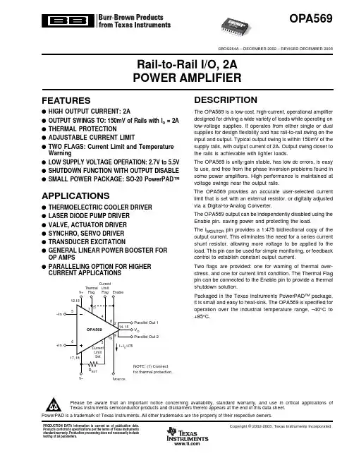
LM2674SIMPLE SWITCHER ®Power Converter High Efficiency 500mA Step-Down Voltage RegulatorGeneral DescriptionThe LM2674series of regulators are monolithic integrated circuits built with a LMDMOS process.These regulators provide all the active functions for a step-down (buck)switching regulator,capable of driving a 500mA load current with excellent line and load regulation.These devices are available in fixed output voltages of 3.3V,5.0V,12V,and an adjustable output version.Requiring a minimum number of external components,these regulators are simple to use and include patented internal frequency compensation (Patent Nos.5,382,918and 5,514,947)and a fixed frequency oscillator.The LM2674series operates at a switching frequency of 260kHz,thus allowing smaller sized filter components than what would be needed with lower frequency switching regu-lators.Because of its very high efficiency (>90%),the cop-per traces on the printed circuit board are the only heat sinking needed.A family of standard inductors for use with the LM2674are available from several different manufacturers.This feature greatly simplifies the design of switch-mode power supplies using these advanced ICs.Also included in the datasheet are selector guides for diodes and capacitors designed to work in switch-mode power supplies.Other features include a guaranteed ±1.5%tolerance on output voltage within specified input voltages and output load conditions,and ±10%on the oscillator frequency.Ex-ternal shutdown is included,featuring typically 50µA stand-by current.The output switch includes current limiting,as well as thermal shutdown for full protection under fault conditions.To simplify the LM2674buck regulator design procedure,there exists computer design software,LM267X Made Simple (version 6.0).Featuresn Efficiency up to 96%n Available in SO-8,8-pin DIP and LLP packages n Computer Design Software LM267X Made Simple (version 6.0)n Simple and easy to design withn Requires only 5external components n Uses readily available standard inductorsn 3.3V,5.0V,12V,and adjustable output versionsn Adjustable version output voltage range:1.21V to 37V n ±1.5%max output voltage tolerance over line and load conditionsn Guaranteed 500mA output load current n 0.25ΩDMOS Output Switchn Wide input voltage range:8V to 40Vn 260kHz fixed frequency internal oscillatorn TTL shutdown capability,low power standby mode n Thermal shutdown and current limit protectionTypical Applicationsn Simple High Efficiency (>90%)Step-Down (Buck)Regulatorn Efficient Pre-Regulator for Linear Regulators n Positive-to-Negative ConverterTypical Application10004101SIMPLE SWITCHER ®is a registered trademark of National Semiconductor Corporation.Windows ®is a registered trademark of Microsoft Corporation.May 2001LM2674SIMPLE SWITCHER Power Converter High Efficiency 500mA Step-Down Voltage Regulator©2001National Semiconductor Corporation Connection Diagrams16-Lead LLP Surface Mount PackageTop View8-Lead PackageTop View10004138LLP PackageSee NSC Package Drawing Number LDA16A10004102SO-8/DIP PackageSee NSC Package Drawing Number MO8A/N08ETABLE 1.Package Marking and Ordering InformationOutput Voltage Order InformationPackage MarkingSupplied as:16Lead LLP12LM2674LD-12S0009B 1000Units on Tape and Reel 12LM2674LDX-12S0009B 4500Units on Tape and Reel 3.3LM2674LD-3.3S000AB 1000Units on Tape and Reel 3.3LM2674LDX-3.3S000AB 4500Units on Tape and Reel 5.0LM2674LD-5.0S000BB 1000Units on Tape and Reel 5.0LM2674LDX-5.0S000BB 4500Units on Tape and Reel ADJ LM2674LD-ADJ S000CB 1000Units on Tape and Reel ADJLM2674LDX-ADJS000CB4500Units on Tape and ReelSO-812LM2674M-122674M-12Shipped in Anti-Static Rails 12LM2674MX-122674M-122500Units on Tape and Reel 3.3LM2674M-3.32674M-3.3Shipped in Anti-Static Rails 3.3LM2674MX-3.32674M-3.32500Units on Tape and Reel 5.0LM2674M-5.02674M-5.0Shipped in Anti-Static Rails 5.0LM2674MX-5.02674M-5.02500Units on Tape and Reel ADJ LM2674M-ADJ 2674M-ADJ Shipped in Anti-Static Rails ADJLM2674MX-ADJ2674M-ADJ2500Units on Tape and ReelDIP12LM2674N-12LM2674N-12Shipped in Anti-Static Rails 3.3LM2674N-3.3LM2674N-3.3Shipped in Anti-Static Rails 5.0LM2674N-5.0LM2674N-5.0Shipped in Anti-Static Rails ADJLM2674N-ADJLM2674N-ADJShipped in Anti-Static RailsL M 2674 2Absolute Maximum Ratings(Note1)If Military/Aerospace specified devices are required,please contact the National Semiconductor Sales Office/ Distributors for availability and specifications.Supply Voltage45V ON/OFF Pin Voltage−0.1V≤V SH≤6V Switch Voltage to Ground−1V Boost Pin Voltage V SW+8V Feedback Pin Voltage−0.3V≤V FB≤14V ESD SusceptibilityHuman Body Model(Note2)2kV Power Dissipation Internally Limited Storage Temperature Range−65˚C to+150˚C Lead TemperatureM PackageVapor Phase(60s)+215˚C Infrared(15s)+220˚C N Package(Soldering,10s)+260˚C LLP Package(See AN-1187)Maximum Junction Temperature+150˚COperating RatingsSupply Voltage 6.5V to40VJunction Temperature Range−40˚C≤T J≤+125˚CElectrical CharacteristicsLM2674-3.3Specifications with standard type face are for TJ=25˚C,and those with bold type face apply over full Operating Temperature Range.Symbol Parameter Conditions Typical Min Max Units(Note4)(Note5)(Note5) SYSTEM PARAMETERS Test Circuit Figure2(Note3)V OUT Output Voltage V IN=8V to40V,I LOAD=20mA to500mA 3.3 3.251/3.201 3.350/3.399V V OUT Output Voltage V IN=6.5V to40V,I LOAD=20mA to250mA 3.3 3.251/3.201 3.350/3.399V ηEfficiency V IN=12V,I LOAD=500mA86% LM2674-5.0Symbol Parameter Conditions Typical Min Max Units(Note4)(Note5)(Note5) SYSTEM PARAMETERS Test Circuit Figure2(Note3)V OUT Output Voltage V IN=8V to40V,I LOAD=20mA to500mA 5.0 4.925/4.850 5.075/5.150V V OUT Output Voltage V IN=6.5V to40V,I LOAD=20mA to250mA 5.0 4.925/4.850 5.075/5.150V ηEfficiency V IN=12V,I LOAD=500mA90% LM2674-12Symbol Parameter Conditions Typical Min Max Units(Note4)(Note5)(Note5) SYSTEM PARAMETERS Test Circuit Figure2(Note3)V OUT Output Voltage V IN=15V to40V,I LOAD=20mA to500mA1211.82/11.6412.18/12.36V ηEfficiency V IN=24V,I LOAD=500mA94% LM2674-ADJSymbol Parameter Conditions Typ Min Max Units(Note4)(Note5)(Note5) SYSTEM PARAMETERS Test Circuit Figure3(Note3)V FB FeedbackVoltage V IN=8V to40V,I LOAD=20mA to500mAV OUT Programmed for5V(see Circuit of Figure3)1.210 1.192/1.174 1.228/1.246VLM26743LM2674-ADJ(Continued)Symbol Parameter ConditionsTyp Min Max Units(Note 4)(Note 5)(Note 5)V FBFeedback Voltage V IN =6.5V to 40V,I LOAD =20mA to 250mA V OUT Programmed for 5V (see Circuit of Figure 3) 1.210 1.192/1.1741.228/1.246V ηEfficiencyV IN =12V,I LOAD =500mA90%All Output Voltage VersionsSpecifications with standard type face are for T J =25˚C,and those with bold type face apply over full Operating Tempera-ture Range .Unless otherwise specified,V IN =12V for the 3.3V,5V,and Adjustable versions and V IN =24V for the 12V ver-sion,and I LOAD =100mA.Symbol ParametersConditionsTyp MinMax Units DEVICE PARAMETERSI QQuiescent CurrentV FEEDBACK =8V2.53.6mAFor 3.3V,5.0V,and ADJ Versions V FEEDBACK =15V 2.5mAFor 12V VersionsI STBY Standby Quiescent Current ON/OFF Pin =0V50100/150µA I CL Current Limit0.80.62/0.5751.2/1.25A I LOutput Leakage CurrentV IN =40V,ON/OFF Pin =0V V SWITCH =0V125µA V SWITCH =−1V,ON/OFF Pin =0V615mA R DS(ON)Switch On-Resistance I SWITCH =500mA 0.250.40/0.60Ωf O Oscillator Frequency Measured at Switch Pin 260225275kHz D Maximum Duty Cycle 95%Minimum Duty Cycle 0%I BIAS Feedback Bias CurrentV FEEDBACK =1.3V ADJ Version Only 85nA V S/D ON/OFF PinVoltage Thesholds 1.40.8 2.0V I S/D ON/OFF Pin Current ON/OFF Pin =0V20737µA θJAThermal ResistanceN Package,Junction to Ambient (Note 6)95˚C/WM Package,Junction to Ambient (Note 6)105Note 1:Absolute Maximum Ratings indicate limits beyond which damage to the device may occur.Operating Ratings indicate conditions for which the device is intended to be functional,but device parameter specifications may not be guaranteed under these conditions.For guaranteed specifications and test conditions,see the Electrical Characteristics.Note 2:The human body model is a 100pF capacitor discharged through a 1.5k Ωresistor into each pin.Note 3:External components such as the catch diode,inductor,input and output capacitors,and voltage programming resistors can affect switching regulator performance.When the LM2674is used as shown in Figures 2,3test circuits,system performance will be as specified by the system parameters section of the Electrical Characteristics.Note 4:Typical numbers are at 25˚C and represent the most likely norm.Note 5:All limits guaranteed at room temperature (standard type face)and at temperature extremes (bold type face).All room temperature limits are 100%production tested.All limits at temperature extremes are guaranteed via correlation using standard Statistical Quality Control (SQC)methods.All limits are used to calculate Average Outgoing Quality Level (AOQL).Note 6:Junction to ambient thermal resistance with approximately 1square inch of printed circuit board copper surrounding the leads.Additional copper area will lower thermal resistance further.See Application Information section in the application note accompanying this datasheet and the thermal model in LM267X Made Simple (version 6.0)software.The value θJ−A for the LLP (LD)package is specifically dependent on PCB trace area,trace material,and the number of layers and thermal vias.For improved thermal resistance and power dissipation for the LLP package,refer to Application Note AN-1187.L M 2674 4Typical PerformanceCharacteristicsNormalizedOutput Voltage Line Regulation Efficiency100041031000410410004105Drain-to-SourceResistance Switch Current LimitOperating Quiescent Current100041061000410710004108Standby Quiescent CurrentON/OFF ThresholdVoltageON/OFF PinCurrent(Sourcing)100041091000411010004111LM26745Typical Performance Characteristics(Continued)Switching FrequencyFeedback Pin Bias CurrentPeak Switch Current100041121000411310004114Dropout Voltage —3.3V Option Dropout Voltage —5.0V Option1000411510004116L M 2674 6LM2674 Block Diagram Array10004117*Active Inductor Patent Number5,514,947†Active Capacitor Patent Number5,382,918FIGURE1.7Typical PerformanceCharacteristics (Circuit of Figure 2)Continuous Mode Switching Waveforms V IN =20V,V OUT =5V,I LOAD =500mA L =100µH,C OUT =100µF,C OUT ESR =0.1ΩDiscontinuous Mode Switching Waveforms V IN =20V,V OUT =5V,I LOAD =300mAL =15µH,C OUT =68µF (2x),C OUT ESR =25m Ω10004118Horizontal Time Base:1µs/divA:V SW Pin Voltage,10V/div.B:Inductor Current,0.2A/divC:Output Ripple Voltage,50mV/div AC-Coupled10004119Horizontal Time Base:1µs/divA:V SW Pin Voltage,10V/div.B:Inductor Current,0.5A/divC:Output Ripple Voltage,20mV/div AC-CoupledLoad Transient Response for Continuous ModeV IN =20V,V OUT =5V,L =100µH,C OUT =100µF,C OUT ESR =0.1ΩLoad Transient Response for Discontinuous ModeV IN =20V,V OUT =5V,L =47µH,C OUT =68µF,C OUT ESR =50m Ω10004120Horizontal Time Base:50µs/divA:Output Voltage,100mV/div,AC-Coupled.B:Load Current:100mA to 500mA Load Pulse10004121Horizontal Time Base:200µs/divA:Output Voltage,100mV/div,AC-Coupled.B:Load Current:100mA to 400mA Load PulseL M 2674 8Test Circuit and Layout Guidelines10004122C IN -22µF,50V Tantalum,Sprague “199D Series”C OUT -47µF,25V Tantalum,Sprague “595D Series”D1-3.3A,50V Schottky Rectifier,IR 30WQ05F L1-68µH Sumida #RCR110D-680L C B -0.01µF,50V CeramicFIGURE 2.Standard Test Circuits and Layout GuidesFixed Output Voltage Versions10004123C IN -22µF,50V Tantalum,Sprague “199D Series”C OUT -47µF,25V Tantalum,Sprague “595D Series”D1-3.3A,50V Schottky Rectifier,IR 30WQ05F L1-68µH Sumida #RCR110D-680L R1-1.5k Ω,1%C B -0.01µF,50V CeramicFor a 5V output,select R2to be 4.75k Ω,1%where V REF =1.21VUse a 1%resistor for best stability.FIGURE 3.Standard Test Circuits and Layout GuidesAdjustable Output Voltage VersionsLM26749LM2674Series Buck Regulator Design Procedure (Fixed Output)PROCEDURE (Fixed Output Voltage Version)EXAMPLE (Fixed Output Voltage Version)To simplify the buck regulator design procedure,NationalSemiconductor is making available computer design software to be used with the SIMPLE SWITCHER line of switchingregulators.LM267X Made Simple (version 6.0)is available on Windows ®3.1,NT,or 95operating systems.Given:Given:V OUT =Regulated Output Voltage (3.3V,5V,or 12V)V OUT =5V V IN (max)=Maximum DC Input Voltage V IN (max)=12V I LOAD (max)=Maximum Load Current I LOAD (max)=500mA 1.Inductor Selection (L1)1.Inductor Selection (L1)A.Select the correct inductor value selection guide from Figure 4,Figure 5or Figure 6(output voltages of 3.3V,5V,or 12V respectively).For all other voltages,see the design procedure for the adjustable version.e the inductor selection guide for the 5V version shown in Figure 5.B.From the inductor value selection guide,identify theinductance region intersected by the Maximum Input Voltage line and the Maximum Load Current line.Each region isidentified by an inductance value and an inductor code (LXX). B.From the inductor value selection guide shown in Figure 5,the inductance region intersected by the 12V horizontal line and the 500mA vertical line is 47µH,and the inductor code is L13.C.Select an appropriate inductor from the four manufacturer’s part numbers listed in Figure 8.Each manufacturer makes a different style of inductor to allow flexibility in meeting various design requirements.Listed below are some of thedifferentiating characteristics of each manufacturer’s inductors:C.The inductance value required is 47µH.From the table in Figure 8,go to the L13line and choose an inductor part number from any of the four manufacturers shown.(In most instances,both through hole and surface mount inductors are available.)Schott:ferrite EP core inductors;these have very low leakage magnetic fields to reduce electro-magnetic interference (EMI)and are the lowest power loss inductorsRenco:ferrite stick core inductors;benefits are typically lowest cost inductors and can withstand E •T and transient peakcurrents above rated value.Be aware that these inductors have an external magnetic field which may generate more EMI than other types of inductors.Pulse:powered iron toroid core inductors;these can also be low cost and can withstand larger than normal E •T and transient peak currents.Toroid inductors have low EMI.Coilcraft:ferrite drum core inductors;these are the smallest physical size inductors,available only as SMT components.Be aware that these inductors also generate EMI —but less than stick inductors.Complete specifications for these inductors are available from the respective manufacturers.A table listing the manufacturers’phone numbers is located in Figure 9.2.Output Capacitor Selection (C OUT )2.Output Capacitor Selection (C OUT )A.Select an output capacitor from the output capacitor table in Figure ing the output voltage and the inductance value found in the inductor selection guide,step 1,locate the appropriate capacitor value and voltage rating.e the 5.0V section in the output capacitor table in Figure 10.Choose a capacitor value and voltage rating from the line that contains the inductance value of 47µH.The capacitance and voltage rating values corresponding to the 47µH inductor are the:L M 2674 10LM2674Series Buck Regulator Design Procedure(Fixed Output)(Continued) PROCEDURE(Fixed Output Voltage Version)EXAMPLE(Fixed Output Voltage Version)The capacitor list contains through-hole electrolytic capacitors from four different capacitor manufacturers and surface mount tantalum capacitors from two different capacitor manufacturers. It is recommended that both the manufacturers and the manufacturer’s series that are listed in the table be used.A table listing the manufacturers’phone numbers is located in Figure11.Surface Mount:68µF/10V Sprague594D Series.100µF/10V AVX TPS Series. Through Hole:68µF/10V Sanyo OS-CON SA Series. 150µF/35V Sanyo MV-GX Series. 150µF/35V Nichicon PL Series.150µF/35V Panasonic HFQ Series.3.Catch Diode Selection(D1)A.In normal operation,the average current of the catch diode is the load current times the catch diode duty cycle,1-D(D is the switch duty cycle,which is approximately the output voltage divided by the input voltage).The largest value of the catch diode average current occurs at the maximum load current and maximum input voltage(minimum D).For normal operation,the catch diode current rating must be at least1.3times greater than its maximum average current.However,if the power supply design must withstand a continuous output short,the diode should have a current rating equal to the maximum current limit of the LM2674.The most stressful condition for this diode is a shorted output condition.3.Catch Diode Selection(D1)A.Refer to the table shown in Figure12.In this example,a1A, 20V Schottky diode will provide the best performance.If the circuit must withstand a continuous shorted output,a higher current Schottky diode is recommended.B.The reverse voltage rating of the diode should be at least1.25times the maximum input voltage.C.Because of their fast switching speed and low forwardvoltage drop,Schottky diodes provide the best performance andefficiency.This Schottky diode must be located close to theLM2674using short leads and short printed circuit traces.4.Input Capacitor(C IN) 4.Input Capacitor(C IN)LM2674LM2674Series Buck Regulator Design Procedure (Fixed Output)(Continued)PROCEDURE (Fixed Output Voltage Version)EXAMPLE (Fixed Output Voltage Version)A low ESR aluminum or tantalum bypass capacitor is needed between the input pin and ground to prevent large voltagetransients from appearing at the input.This capacitor should be located close to the IC using short leads.In addition,the RMS current rating of the input capacitor should be selected to be at least 1⁄2the DC load current.The capacitor manufacturer data sheet must be checked to assure that this current rating is not exceeded.The curves shown in Figure 14show typical RMS current ratings for several different aluminum electrolytic capacitor values.A parallel connection of two or morecapacitors may be required to increase the total minimum RMS current rating to suit the application requirements.For an aluminum electrolytic capacitor,the voltage rating should be at least 1.25times the maximum input voltage.Caution must be exercised if solid tantalum capacitors are used.The tantalum capacitor voltage rating should be twice the maximum input voltage.The tables in Figure 15show the recommendedapplication voltage for AVX TPS and Sprague 594D tantalum capacitors.It is also recommended that they be surge current tested by the manufacturer.The TPS series available from AVX,and the 593D and 594D series from Sprague are all surgecurrent tested.Another approach to minimize the surge current stresses on the input capacitor is to add a small inductor in series with the input supply line.Use caution when using ceramic capacitors for input bypassing,because it may cause severe ringing at the V IN pin.The important parameters for the input capacitor are the input voltage rating and the RMS current rating.With a maximum input voltage of 12V,an aluminum electrolytic capacitor with a voltage rating greater than 15V (1.25x V IN )would be needed.The next higher capacitor voltage rating is 16V.The RMS current rating requirement for the input capacitor in a buck regulator is approximately 1⁄2the DC load current.In this example,with a 500mA load,a capacitor with an RMS current rating of at least 250mA is needed.The curves shown in Figure 14can be used to select an appropriate input capacitor.From the curves,locate the 16V line and note which capacitor values have RMS current ratings greater than 250mA.For a through hole design,a 100µF/16V electrolytic capacitor (Panasonic HFQ series,Nichicon PL,Sanyo MV-GX series or equivalent)would be adequate.Other types or othermanufacturers’capacitors can be used provided the RMS ripple current ratings are adequate.Additionally,for a completesurface mount design,electrolytic capacitors such as the Sanyo CV-C or CV-BS and the Nichicon WF or UR and the NIC Components NACZ series could be considered.For surface mount designs,solid tantalum capacitors can be used,but caution must be exercised with regard to the capacitor surge current rating and voltage rating.In this example,checking Figure 15,and the Sprague 594D series datasheet,a Sprague 594D 15µF,25V capacitor is adequate.5.Boost Capacitor (C B )5.Boost Capacitor (C B )This capacitor develops the necessary voltage to turn the switch gate on fully.All applications should use a 0.01µF,50V ceramic capacitor.For this application,and all applications,use a 0.01µF,50V ceramic capacitor.L M 2674INDUCTOR VALUE SELECTION GUIDES(For Continuous Mode Operation)10004126 FIGURE4.LM2674-3.310004127 FIGURE5.LM2674-5.010004128FIGURE6.LM2674-1210004129FIGURE7.LM2674-ADJLM2674INDUCTOR VALUE SELECTION GUIDES(For Continuous Mode Operation)(Continued)Ind.Ref.Desg.Inductance (µH)Current (A)SchottRencoPulse Engineering Coilcraft Through Surface ThroughSurface Through Surface Surface HoleMountHoleMountHoleMountMountL21500.216714392067144290RL-5470-4RL1500-150PE-53802PE-53802-S DO1608-154L31000.266714393067144300RL-5470-5RL1500-100PE-53803PE-53803-S DO1608-104L4680.326714394067144310RL-1284-68-43RL1500-68PE-53804PE-53804-S DO1608-683L5470.376714831067148420RL-1284-47-43RL1500-47PE-53805PE-53805-S DO1608-473L6330.446714832067148430RL-1284-33-43RL1500-33PE-53806PE-53806-S DO1608-333L7220.526714833067148440RL-1284-22-43RL1500-22PE-53807PE-53807-S DO1608-223L92200.326714396067144330RL-5470-3RL1500-220PE-53809PE-53809-S DO3308-224L101500.396714397067144340RL-5470-4RL1500-150PE-53810PE-53810-S DO3308-154L111000.486714398067144350RL-5470-5RL1500-100PE-53811PE-53811-S DO3308-104L12680.586714399067144360RL-5470-6RL1500-68PE-53812PE-53812-S DO3308-683L13470.706714400067144380RL-5470-7RL1500-47PE-53813PE-53813-S DO3308-473L14330.836714834067148450RL-1284-33-43RL1500-33PE-53814PE-53814-S DO3308-333L15220.996714835067148460RL-1284-22-43RL1500-22PE-53815PE-53815-S DO3308-223L182200.556714404067144420RL-5471-2RL1500-220PE-53818PE-53818-S DO3316-224L191500.666714405067144430RL-5471-3RL1500-150PE-53819PE-53819-S DO3316-154L201000.826714406067144440RL-5471-4RL1500-100PE-53820PE-53820-S DO3316-104L21680.996714407067144450RL-5471-5RL1500-68PE-53821PE-53821-S DO3316-683FIGURE 8.Inductor Manufacturers’Part Numbers Coilcraft Inc.Phone (800)322-2645FAX (708)639-1469Coilcraft Inc.,Europe Phone +441236730595FAX +441236730627Pulse Engineering Inc.Phone (619)674-8100FAX (619)674-8262Pulse Engineering Inc.,Phone +3539324107EuropeFAX +3539324459Renco Electronics Inc.Phone (800)645-5828FAX (516)586-5562Schott Corp.Phone (612)475-1173FAX(612)475-1786FIGURE 9.Inductor Manufacturers’Phone NumbersL M 2674INDUCTOR VALUE SELECTION GUIDES(For Continuous Mode Operation)(Continued)Output Voltage(V)Inductance(µH)Output CapacitorSurface Mount Through HoleSprague AVX TPS Sanyo OS-CON Sanyo MV-GX Nichicon Panasonic594D Series Series SA Series Series PL Series HFQ Series (µF/V)(µF/V)(µF/V)(µF/V)(µF/V)(µF/V)3.322120/6.3100/10100/10330/35330/35330/35 33120/6.3100/1068/10220/35220/35220/35 4768/10100/1068/10150/35150/35150/35 68120/6.3100/10100/10120/35120/35120/35 100120/6.3100/10100/10120/35120/35120/35 150120/6.3100/10100/10120/35120/35120/355.022100/16100/10100/10330/35330/35330/35 3368/101001068/10220/35220/35220/35 4768/10100/1068/10150/35150/35150/35 68100/16100/10100/10120/35120/35120/35 100100/16100/10100/10120/35120/35120/35 150100/16100/10100/10120/35120/35120/351222120/20(2x)68/2068/20330/35330/35330/353368/2568/2068/20220/35220/35220/354747/2068/2047/20150/35150/35150/356847/2068/2047/20120/35120/35120/3510047/2068/2047/20120/35120/35120/3515047/2068/2047/20120/35120/35120/3522047/2068/2047/20120/35120/35120/35FIGURE10.Output Capacitor TableNichicon Corp.Phone(847)843-7500FAX(847)843-2798Panasonic Phone(714)373-7857FAX(714)373-7102AVX Corp.Phone(845)448-9411FAX(845)448-1943Sprague/Vishay Phone(207)324-4140FAX(207)324-7223Sanyo Corp.Phone(619)661-6322FAX(619)661-1055FIGURE11.Capacitor Manufacturers’Phone NumbersLM2674INDUCTOR VALUE SELECTION GUIDES(For Continuous Mode Operation)(Continued)V R 500mA Diodes3A Diodes Surface Through Surface Through Mount Hole Mount Hole 20V SK121N5817SK321N5820B120SR102SR30230VSK131N5818SK331N5821B13011DQ0330WQ03F 31DQ03MBRS130SR10340VSK141N5819SK341N5822B14011DQ0430BQ040MBR340MBRS140SR10430WQ04F 31DQ0410BQ040MBRS340SR30410MQ040MBRD34015MQ04050VSK15MBR150SK35MBR350B15011DQ0530WQ05F31DQ0510BQ050SR105SR305FIGURE 12.Schottky Diode Selection Table International Rectifier Corp.Phone (310)322-3331FAX (310)322-3332Motorola,Inc.Phone (800)521-6274FAX (602)244-6609General Instruments Corp.Phone (516)847-3000FAX (516)847-3236Diodes,Inc.Phone (805)446-4800FAX(805)446-4850FIGURE 13.Diode Manufacturers’Phone Numbers10004130FIGURE 14.RMS Current Ratings for Low ESR Electrolytic Capacitors (Typical)L M 2674LM2674 INDUCTOR VALUE SELECTION GUIDES(For Continuous Mode Operation)(Continued)AVX TPSRecommended VoltageApplication Voltage Rating+85˚C Rating3.3 6.3510102012251535Sprague594DRecommended VoltageApplication Voltage Rating+85˚C Rating2.543.3 6.35108161220182524352950FIGURE15.Recommended Application Voltage for AVX TPS andSprague594D Tantalum Chip Capacitors Derated for85˚C.LM2674Series Buck Regulator Design Procedure (Adjustable Output)PROCEDURE (Adjustable Output Voltage Version)EXAMPLE (Adjustable Output Voltage Version)To simplify the buck regulator design procedure,NationalSemiconductor is making available computer design software to be used with the SIMPLE SWITCHER line of switchingregulators.LM267X Made Simple (version 6.0)is available for use on Windows 3.1,NT,or 95operating systems.Given:Given:V OUT =Regulated Output Voltage V OUT =20V V IN (max)=Maximum Input Voltage V IN (max)=28V I LOAD (max)=Maximum Load CurrentI LOAD (max)=500mAF =Switching Frequency (Fixed at a nominal 260kHz).F =Switching Frequency (Fixed at a nominal 260kHz).1.Programming Output Voltage (Selecting R 1and R 2,as shown in Figure 3)1.Programming Output Voltage (Selecting R 1and R 2,as shown in Figure 3)Use the following formula to select the appropriate resistor values.Select R 1to be 1k Ω,1%.Solve for R 2.where V REF =1.21VSelect a value for R 1between 240Ωand 1.5k Ω.The lower resistor values minimize noise pickup in the sensitive feedback pin.(For the lowest temperature coefficient and the best stability with time,use 1%metal film resistors.)R 2=1k (16.53−1)=15.53k Ω,closest 1%value is 15.4k Ω.R 2=15.4k Ω.2.Inductor Selection (L1) 2.Inductor Selection (L1)A.Calculate the inductor Volt •microsecond constant E •T (V •µs),from the following formula:A.Calculate the inductor Volt •microsecond constant (E •T),where V SAT =internal switch saturation voltage=0.25V and V D =diode forward voltage drop =0.5Ve the E •T value from the previous formula and match it with the E •T number on the vertical axis of the Inductor Value Selection Guide shown in Figure 7.B.E •T =21.6(V •µs)C.On the horizontal axis,select the maximum load current. C.I LOAD (max)=500mAD.Identify the inductance region intersected by the E •T value and the Maximum Load Current value.Each region is identified by an inductance value and an inductor code (LXX).D.From the inductor value selection guide shown in Figure 7,the inductance region intersected by the 21.6(V •µs)horizontal line and the 500mA vertical line is 100µH,and the inductor code is L20.E.Select an appropriate inductor from the four manufacturer’s part numbers listed in Figure 8.For information on the different types of inductors,see the inductor selection in the fixed output voltage design procedure.E.From the table in Figure 8,locate line L20,and select an inductor part number from the list of manufacturers part numbers.3.Output Capacitor Selection (C OUT )3.Output Capacitor SeIection (C OUT )A.Select an output capacitor from the capacitor code selection guide in Figure ing the inductance value found in theinductor selection guide,step 1,locate the appropriate capacitor code corresponding to the desired output voltage.e the appropriate row of the capacitor code selectionguide,in Figure 16.For this example,use the 15–20V row.The capacitor code corresponding to an inductance of 100µH is C20.L M 2674。
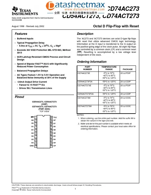
Data sheet acquired from Harris SemiconductorSCHS249BFeatures•Buffered Inputs•Typical Propagation Delay- 6.5ns at V CC = 5V , T A = 25o C, C L = 50pF•Exceeds 2kV ESD Protection MIL-STD-883, Method 3015•SCR-Latchup-Resistant CMOS Process and Circuit Design •Speed of Bipolar FAST™/AS/S with Significantly Reduced Power Consumption •Balanced Propagation Delays•AC Types Feature 1.5V to 5.5V Operation and Balanced Noise Immunity at 30% of the Supply •±24mA Output Drive Current -Fanout to 15 FAST™ ICs-Drives 50Ω Transmission LinesPinoutCD54AC273, CD54ACT273(CDIP)CD74AC273, CD74ACT273(PDIP , SOIC)TOP VIEWDescriptionThe ’AC273and ’ACT273devices are octal D-type flip-flops with reset that utilize advanced CMOS logic rmation at the D input is transferred to the Q output on the positive-going edge of the clock pulse.All eight flip-flops are controlled by a common clock (CP)and a common reset (MR).Resetting is accomplished by a low voltage level independent of the clock.1112131415161718201910987654321MR Q0D0D1Q1Q2D3D2Q3GND V CC D7D6Q6Q7Q5D5D4Q4CPOrdering InformationPART NUMBER TEMPERATURERANGE PACKAGE CD74AC273E0o C to 70o C -40o C to 85o C -55o C to 125o C 20 Ld PDIPCD54AC273F3A -55o C to 125o C 20 Ld CDIP CD74ACT273E0o C to 70o C -40o C to 85o C -55o C to 125o C 20 Ld PDIPCD54ACT273F3A -55o C to 125o C 20 Ld CDIP CD74AC273M0o C to 70o C -40o C to 85o C -55o C to 125o C 20 Ld SOICCD74ACT273M 0o C to 70o C -40o C to 85o C -55o C to 125o C20 Ld SOICNOTES:1.When ordering,use the entire part number.Add the suffix 96to obtain the variant in the tape and reel.2.Wafer and die for this part number is available which meets allelectrical specifications.Please contact your local sales office for ordering information.August 1998 - Revised July 2002CD54AC273, CD74AC273CD54ACT273, CD74ACT273Octal D Flip-Flop with ResetFunctional DiagramTRUTH TABLE INPUTSOUTPUTSRESET (MR)CLOCK CP DATA Dn Qn L X X L H ↑H H H ↑L L HLXQ0H =High level (steady state),L =Low level (steady state),X =Irrel-evant,↑=Transition from Low to High level,Q0=The level of Q before the indicated steady-state input conditions were estab-lished.Q0Q1Q2Q3Q4Q5Q6Q7RESET MRD0D1D2D3D4D5D6D7CLOCKCPDATA INPUTSDATAOUTPUTSAbsolute Maximum Ratings Thermal InformationDC Supply Voltage, V CC. . . . . . . . . . . . . . . . . . . . . . . .-0.5V to 6V DC Input Diode Current, I IKFor V I < -0.5V or V I > V CC + 0.5V. . . . . . . . . . . . . . . . . . . . . .±20mA DC Output Diode Current, I OKFor V O < -0.5V or V O > V CC + 0.5V . . . . . . . . . . . . . . . . . . . .±50mA DC Output Source or Sink Current per Output Pin, I OFor V O > -0.5V or V O < V CC + 0.5V . . . . . . . . . . . . . . . . . . . .±50mA DC V CC or Ground Current, I CC or I GND (Note 3) . . . . . . . . .±100mA Operating ConditionsTemperature Range, T A . . . . . . . . . . . . . . . . . . . . . .-55o C to 125o C Supply Voltage Range, V CC (Note 4)AC T ypes. . . . . . . . . . . . . . . . . . . . . . . . . . . . . . . . . . .1.5V to 5.5V ACT T ypes . . . . . . . . . . . . . . . . . . . . . . . . . . . . . . . . .4.5V to 5.5V DC Input or Output Voltage, V I, V O . . . . . . . . . . . . . . . . .0V to V CC Input Rise and Fall Slew Rate, dt/dvAC T ypes, 1.5V to 3V . . . . . . . . . . . . . . . . . . . . . . . . .50ns (Max) AC T ypes, 3.6V to 5.5V. . . . . . . . . . . . . . . . . . . . . . . .20ns (Max) ACT T ypes, 4.5V to 5.5V. . . . . . . . . . . . . . . . . . . . . . .10ns (Max)Thermal Resistance,θJA(Typical, Note 5)E Package. . . . . . . . . . . . . . . . . . . . . . . . . . . . . . . . . . . . .69o C/W M Package. . . . . . . . . . . . . . . . . . . . . . . . . . . . . . . . . . . . .58o C/W Maximum Junction T emperature (Plastic Package) . . . . . . . . . .150o C Maximum Storage Temperature Range . . . . . . . . . .-65o C to 150o C Maximum Lead Temperature (Soldering 10s). . . . . . . . . . . . .300o CCAUTION:Stresses above those listed in“Absolute Maximum Ratings”may cause permanent damage to the device.This is a stress only rating and operation of the device at these or any other conditions above those indicated in the operational sections of this specification is not implied.NOTES:3.For up to 4 outputs per device, add±25mA for each additional output.4.Unless otherwise specified, all voltages are referenced to ground.5.The package thermal impedance is calculated in accordance with JESD 51.DC Electrical SpecificationsPARAMETER SYMBOLTESTCONDITIONS VCC(V)25o C-40o C TO85o C-55o C TO125o CUNITS V I(V)I O(mA)MIN MAX MIN MAX MIN MAXAC TYPESHigh Level Input Voltage V IH-- 1.5 1.2- 1.2- 1.2-V3 2.1- 2.1- 2.1-V5.5 3.85- 3.85- 3.85-V Low Level Input Voltage V IL-- 1.5-0.3-0.3-0.3V3-0.9-0.9-0.9V5.5- 1.65- 1.65- 1.65V High Level Output Voltage V OH V IH or V IL-0.05 1.5 1.4- 1.4- 1.4-V-0.053 2.9- 2.9- 2.9-V-0.05 4.5 4.4- 4.4- 4.4-V-43 2.58- 2.48- 2.4-V-24 4.5 3.94- 3.8- 3.7-V-75(Note 6, 7)5.5-- 3.85---V-50(Note 6, 7)5.5---- 3.85-VLow Level Output VoltageV OLV IH or V IL0.05 1.5-0.1-0.1-0.1V 0.053-0.1-0.1-0.1V 0.05 4.5-0.1-0.1-0.1V 123-0.36-0.44-0.5V 24 4.5-0.36-0.44-0.5V 75(Note 6, 7) 5.5--- 1.65--V 50(Note 6, 7)5.5----- 1.65V Input Leakage Current I I V CC or GND - 5.5-±0.1-±1-±1µA Quiescent Supply Current MSI I CCV CC or GND5.5-8-80-160µAACT TYPESHigh Level Input Voltage V IH -- 4.5 to 5.52-2-2-V Low Level Input Voltage V IL -- 4.5 to 5.5-0.8-0.8-0.8V High Level Output VoltageV OHV IH or V IL-0.05 4.5 4.4- 4.4- 4.4-V -24 4.5 3.94- 3.8- 3.7-V -75(Note 6, 7) 5.5-- 3.85---V -50(Note 6, 7)5.5---- 3.85-V Low Level Output VoltageV OLV IH or V IL0.05 4.5-0.1-0.1-0.1V 24 4.5-0.36-0.44-0.5V 75(Note 6, 7) 5.5--- 1.65--V 50(Note 6, 7)5.5----- 1.65V Input Leakage Current I I V CC or GND - 5.5-±0.1-±1-±1µA Quiescent Supply Current MSII CC V CC or GND 0 5.5-8-80-160µA Additional Supply Current per Input Pin TTL Inputs High 1 Unit Load ∆I CCV CC -2.1- 4.5 to 5.5- 2.4- 2.8-3mANOTES:6.Test one output at a time for a 1-second maximum duration.Measurement is made by forcing current and measuring voltage to minimize power dissipation.7.Test verifies a minimum 50Ω transmission-line-drive capability at 85o C, 75Ω at 125o C.ACT Input Load TableINPUT UNIT LOADDn 0.5MR 0.57CP1NOTE:Unit load is ∆I CC limit specified in DC Electrical Specifications T able, e.g., 2.4mA max at 25o C.DC Electrical Specifications(Continued)PARAMETERSYMBOL TEST CONDITIONSV CC (V)25o C -40o C TO 85o C -55o C TO 125o C UNITS V I (V)I O (mA)MIN MAX MIN MAX MIN MAXPrerequisite For Switching FunctionPARAMETER SYMBOL V CC (V)-40o C TO 85o C-55o C TO 125o CUNITS MIN MAX MIN MAXAC TYPESData to CP Set-Up Time t SU 1.52-2-ns3.3(Note 9)2-2-ns5(Note 10)2-2-ns Hold Time t H 1.52-2-ns3.32-2-ns52-2-ns Removal Time,MR to CP t REM 1.52-2-ns3.32-2-ns52-2-ns MR Pulse Width t W 1.555-63-ns3.3 6.1-7-ns5 4.4-5-ns CP Pulse Width t W 1.555-63-ns3.3 6.1-7-ns5 4.4-5-ns CP Frequency f MAX 1.59-8-MHz3.381-71-MHz5114-100-MHz ACT TYPESData to CP Set-Up Time t SU5(Note 10)2-2-ns Hold Time t H52-2-ns Removal Time MR to CP t REM52-2-ns MR Pulse Width t W5 4.4-5-ns CP Pulse Width t W5 5.3-6-ns CP Frequency f MAX597-85-MHz Switching Specifications Input t r, t f = 3ns, C L= 50pF (Worst Case)PARAMETER SYMBOL V CC (V)-40o C TO 85o C-55o C TO 125o CUNITS MIN TYP MAX MIN TYP MAXAC TYPESPropagation Delay, CP to Qn t PLH, t PHL 1.5--154--169ns3.3(Note 9)4.9-17.2 4.7-18.9ns5(Note 10)3.5-12.3 3.4-13.5nsPropagation Delay,MR to Qnt PLH , t PHL1.5--154--169ns 3.3 4.9-17.2 4.7-18.9ns 53.5-12.3 3.4-13.5ns Input CapacitanceC I ---10--10pF Power Dissipation Capacitance C PD (Note 11)--45--45-pFACT TYPES Propagation Delay,CP to Qnt PLH , t PHL 5(Note 10)3.5-12.3 3.4-13.5ns Propagation Delay,MR to Qn t PLH , t PHL5 3.5-12.3 3.4-13.5ns Input CapacitanceC I ---10--10pF Power Dissipation Capacitance C PD (Note 11)--45--45-pFNOTES:8.Limits tested 100%.9.3.3V Min is at 3.6V, Max is at 3V.10.5V Min is at 5.5V, Max is at 4.5V.11.C PD is used to determine the dynamic power consumption per flip-flop.AC: P D = C PD V CC 2 f i =∑ (C L V CC 2 f o )ACT:P D =C PD V CC 2f i +∑(C L V CC 2f o )+V CC ∆I CC where f i =input frequency,f o =output frequency,C L =output load capacitance,V CC = supply voltage.FIGURE 1.PROPAGATION DELAY TIMES AND CLOCKPULSE WIDTH FIGURE 2.PREREQUISITE AND PROPAGATION DELAYTIMES FOR MASTER RESETSwitching Specifications Input t r , t f = 3ns, C L = 50pF (Worst Case)(Continued)PARAMETERSYMBOL V CC (V)-40o C TO 85o C-55o C TO 125o CUNITS MIN TYP MAX MIN TYP MAX 90%t f t r V SV S V SV SV St PLHt PHLt W 10%10%CP INPUT LEVEL QMR CPINPUT LEVELV SQV St REMV SV St PLHt WGNDINPUT(Q)FIGURE 3.PREREQUISITE FOR CLOCKDV S V S V SV S V S V St H (H)t SU (L)t H (L)t SU (H)CPOUTPUT LEVELDUT OUTPUTR L (NOTE)OUTPUT LOAD500ΩC L 50pFNOTE:For AC Series Only: When V CC = 1.5V , R L = 1k Ω.FIGURE 4.PROPAGATION DELAY TIMESACACT Input LevelV CC 3V Input Switching Voltage, V S 0.5 V CC 1.5V Output Switching Voltage, V S0.5 V CC0.5 V CCPACKAGING INFORMATIONOrderable Device Status(1)PackageType PackageDrawingPins PackageQtyEco Plan(2)Lead/Ball Finish MSL Peak Temp(3)CD54AC273F3A ACTIVE CDIP J201TBD A42N/A for Pkg Type CD54ACT273F3A ACTIVE CDIP J201TBD A42N/A for Pkg Type CD74AC273E ACTIVE PDIP N2020Pb-Free(RoHS)CU NIPDAU N/A for Pkg TypeCD74AC273EE4ACTIVE PDIP N2020Pb-Free(RoHS)CU NIPDAU N/A for Pkg TypeCD74AC273M ACTIVE SOIC DW2025Green(RoHS&no Sb/Br)CU NIPDAU Level-1-260C-UNLIMCD74AC273M96ACTIVE SOIC DW202000Green(RoHS&no Sb/Br)CU NIPDAU Level-1-260C-UNLIMCD74AC273M96E4ACTIVE SOIC DW202000Green(RoHS&no Sb/Br)CU NIPDAU Level-1-260C-UNLIMCD74AC273M96G4ACTIVE SOIC DW202000Green(RoHS&no Sb/Br)CU NIPDAU Level-1-260C-UNLIMCD74AC273ME4ACTIVE SOIC DW2025Green(RoHS&no Sb/Br)CU NIPDAU Level-1-260C-UNLIMCD74AC273MG4ACTIVE SOIC DW2025Green(RoHS&no Sb/Br)CU NIPDAU Level-1-260C-UNLIMCD74ACT273E ACTIVE PDIP N2020Pb-Free(RoHS)CU NIPDAU N/A for Pkg TypeCD74ACT273EE4ACTIVE PDIP N2020Pb-Free(RoHS)CU NIPDAU N/A for Pkg TypeCD74ACT273M ACTIVE SOIC DW2025Green(RoHS&no Sb/Br)CU NIPDAU Level-1-260C-UNLIMCD74ACT273M96ACTIVE SOIC DW202000Green(RoHS&no Sb/Br)CU NIPDAU Level-1-260C-UNLIMCD74ACT273M96E4ACTIVE SOIC DW202000Green(RoHS&no Sb/Br)CU NIPDAU Level-1-260C-UNLIMCD74ACT273M96G4ACTIVE SOIC DW202000Green(RoHS&no Sb/Br)CU NIPDAU Level-1-260C-UNLIMCD74ACT273ME4ACTIVE SOIC DW2025Green(RoHS&no Sb/Br)CU NIPDAU Level-1-260C-UNLIMCD74ACT273MG4ACTIVE SOIC DW2025Green(RoHS&no Sb/Br)CU NIPDAU Level-1-260C-UNLIMCD74ACT273PW ACTIVE TSSOP PW2070Green(RoHS&no Sb/Br)CU NIPDAU Level-1-260C-UNLIMCD74ACT273PWE4ACTIVE TSSOP PW2070Green(RoHS&no Sb/Br)CU NIPDAU Level-1-260C-UNLIMCD74ACT273PWG4ACTIVE TSSOP PW2070Green(RoHS&no Sb/Br)CU NIPDAU Level-1-260C-UNLIMCD74ACT273PWR ACTIVE TSSOP PW202000Green(RoHS&no Sb/Br)CU NIPDAU Level-1-260C-UNLIMCD74ACT273PWRE4ACTIVE TSSOP PW202000Green(RoHS&no Sb/Br)CU NIPDAU Level-1-260C-UNLIMCD74ACT273PWRG4ACTIVE TSSOP PW202000Green(RoHS&no Sb/Br)CU NIPDAU Level-1-260C-UNLIMCD74ACT273SM96ACTIVE SSOP DB202000Green(RoHS&no Sb/Br)CU NIPDAU Level-1-260C-UNLIMCD74ACT273SM96E4ACTIVE SSOP DB202000Green(RoHS&CU NIPDAU Level-1-260C-UNLIMOrderable Device Status(1)PackageType PackageDrawingPins PackageQtyEco Plan(2)Lead/Ball Finish MSL Peak Temp(3)no Sb/Br)CD74ACT273SM96G4ACTIVE SSOP DB202000Green(RoHS&no Sb/Br)CU NIPDAU Level-1-260C-UNLIM(1)The marketing status values are defined as follows:ACTIVE:Product device recommended for new designs.LIFEBUY:TI has announced that the device will be discontinued,and a lifetime-buy period is in effect.NRND:Not recommended for new designs.Device is in production to support existing customers,but TI does not recommend using this part in a new design.PREVIEW:Device has been announced but is not in production.Samples may or may not be available.OBSOLETE:TI has discontinued the production of the device.(2)Eco Plan-The planned eco-friendly classification:Pb-Free(RoHS),Pb-Free(RoHS Exempt),or Green(RoHS&no Sb/Br)-please check /productcontent for the latest availability information and additional product content details.TBD:The Pb-Free/Green conversion plan has not been defined.Pb-Free(RoHS):TI's terms"Lead-Free"or"Pb-Free"mean semiconductor products that are compatible with the current RoHS requirements for all6substances,including the requirement that lead not exceed0.1%by weight in homogeneous materials.Where designed to be soldered at high temperatures,TI Pb-Free products are suitable for use in specified lead-free processes.Pb-Free(RoHS Exempt):This component has a RoHS exemption for either1)lead-based flip-chip solder bumps used between the die and package,or2)lead-based die adhesive used between the die and leadframe.The component is otherwise considered Pb-Free(RoHS compatible)as defined above.Green(RoHS&no Sb/Br):TI defines"Green"to mean Pb-Free(RoHS compatible),and free of Bromine(Br)and Antimony(Sb)based flame retardants(Br or Sb do not exceed0.1%by weight in homogeneous material)(3)MSL,Peak Temp.--The Moisture Sensitivity Level rating according to the JEDEC industry standard classifications,and peak solder temperature.Important Information and Disclaimer:The information provided on this page represents TI's knowledge and belief as of the date that it is provided.TI bases its knowledge and belief on information provided by third parties,and makes no representation or warranty as to the accuracy of such information.Efforts are underway to better integrate information from third parties.TI has taken and continues to take reasonable steps to provide representative and accurate information but may not have conducted destructive testing or chemical analysis on incoming materials and chemicals.TI and TI suppliers consider certain information to be proprietary,and thus CAS numbers and other limited information may not be available for release.In no event shall TI's liability arising out of such information exceed the total purchase price of the TI part(s)at issue in this document sold by TI to Customer on an annual basis.TAPE AND REELINFORMATION*All dimensionsare nominalDevicePackage Type Package Drawing Pins SPQReel Diameter (mm)Reel Width W1(mm)A0(mm)B0(mm)K0(mm)P1(mm)W (mm)Pin1Quadrant CD74AC273M96SOIC DW 202000330.024.410.813.0 2.712.024.0Q1CD74ACT273M96SOIC DW 202000330.024.410.813.0 2.712.024.0Q1CD74ACT273PWR TSSOP PW 202000330.016.4 6.957.1 1.68.016.0Q1CD74ACT273SM96SSOPDB202000330.016.48.27.52.512.016.0Q1PACKAGE MATERIALS INFORMATION11-Mar-2008*Alldimensions are nominal DevicePackage Type Package Drawing Pins SPQ Length (mm)Width (mm)Height (mm)CD74AC273M96SOIC DW 202000346.0346.041.0CD74ACT273M96SOIC DW 202000346.0346.041.0CD74ACT273PWRTSSOP PW 202000346.0346.033.0CD74ACT273SM96SSOP DB 202000346.0346.033.0PACKAGE MATERIALS INFORMATION 11-Mar-2008Pack Materials-Page 2IMPORTANT NOTICETexas Instruments Incorporated and its subsidiaries(TI)reserve the right to make corrections,modifications,enhancements,improvements, and other changes to its products and services at any time and to discontinue any product or service without notice.Customers should obtain the latest relevant information before placing orders and should verify that such information is current and complete.All products are sold subject to TI’s terms and conditions of sale supplied at the time of order acknowledgment.TI warrants performance of its hardware products to the specifications applicable at the time of sale in accordance with TI’s standard warranty.Testing and other quality control techniques are used to the extent TI deems necessary to support this warranty.Except where mandated by government requirements,testing of all parameters of each product is not necessarily performed.TI assumes no liability for applications assistance or customer product design.Customers are responsible for their products and applications using TI components.To minimize the risks associated with customer products and applications,customers should provide adequate design and operating safeguards.TI does not warrant or represent that any license,either express or implied,is granted under any TI patent right,copyright,mask work right, or other TI intellectual property right relating to any combination,machine,or process in which TI products or services are rmation published by TI regarding third-party products or services does not constitute a license from TI to use such products or services or a warranty or endorsement e of such information may require a license from a third party under the patents or other intellectual property of the third party,or a license from TI under the patents or other intellectual property of TI.Reproduction of TI information in TI data books or data sheets is permissible only if reproduction is without alteration and is accompanied by all associated warranties,conditions,limitations,and notices.Reproduction of this information with alteration is an unfair and deceptive business practice.TI is not responsible or liable for such altered rmation of third parties may be subject to additional restrictions.Resale of TI products or services with statements different from or beyond the parameters stated by TI for that product or service voids all express and any implied warranties for the associated TI product or service and is an unfair and deceptive business practice.TI is not responsible or liable for any such statements.TI products are not authorized for use in safety-critical applications(such as life support)where a failure of the TI product would reasonably be expected to cause severe personal injury or death,unless officers of the parties have executed an agreement specifically governing such use.Buyers represent that they have all necessary expertise in the safety and regulatory ramifications of their applications,and acknowledge and agree that they are solely responsible for all legal,regulatory and safety-related requirements concerning their products and any use of TI products in such safety-critical applications,notwithstanding any applications-related information or support that may be provided by TI.Further,Buyers must fully indemnify TI and its representatives against any damages arising out of the use of TI products in such safety-critical applications.TI products are neither designed nor intended for use in military/aerospace applications or environments unless the TI products are specifically designated by TI as military-grade or"enhanced plastic."Only products designated by TI as military-grade meet military specifications.Buyers acknowledge and agree that any such use of TI products which TI has not designated as military-grade is solely at the Buyer's risk,and that they are solely responsible for compliance with all legal and regulatory requirements in connection with such use. TI products are neither designed nor intended for use in automotive applications or environments unless the specific TI products are designated by TI as compliant with ISO/TS16949requirements.Buyers acknowledge and agree that,if they use any non-designated products in automotive applications,TI will not be responsible for any failure to meet such requirements.Following are URLs where you can obtain information on other Texas Instruments products and application solutions:Products ApplicationsAmplifiers AudioData Converters AutomotiveDLP®Products BroadbandDSP Digital ControlClocks and Timers MedicalInterface MilitaryLogic Optical NetworkingPower Mgmt SecurityMicrocontrollers TelephonyRFID Video&ImagingRF/IF and ZigBee®Solutions WirelessMailing Address:Texas Instruments,Post Office Box655303,Dallas,Texas75265Copyright©2009,Texas Instruments Incorporated。
FEATURESRGY PACKAGE (TOP VIEW)2A119SDA 3RESET 18SCL 4INT017INT 5SD016SC36SC015SD37INT114INT38SD113SC29SC112SD2110A 0G N D2011I N T 2V C CRESET INT0SD0SC0INT1INT SC3SD3INT3SC2RGW PACKAGE (TOP VIEW)S D A S C LA 1A 0V C CDGV ,DW,OR PW PACKAGE(TOP VIEW)DESCRIPTION/ORDERING INFORMATION•1-of-4Bidirectional Translating Switches •No Glitch on Power Up •I 2C Bus and SMBus Compatible •Supports Hot Insertion •Four Active-Low Interrupt Inputs •Low Standby Current•Active-Low Interrupt Output •Operating Power-Supply Voltage Range of 2.3V to 5.5V•Active-Low Reset Input• 5.5-V Tolerant Inputs•Two Address Pins,Allowing up to Four Devices on the I 2C Bus•0to 400-kHz Clock Frequency•Channel Selection Via I 2C Bus,In Any •Latch-Up Performance Exceeds 100mA Per CombinationJESD 78•Power Up With All Switch Channels •ESD Protection Exceeds JESD 22Deselected–2000-V Human-Body Model (A114-A)•Low R ON Switches–200-V Machine Model (A115-A)•Allows Voltage-Level Translation Between –1000-V Charged-Device Model (C101)1.8-V,2.5-V,3.3-V,and 5-V BusesThe PCA9545A is a quad bidirectional translating switch controlled via the I 2C bus.The SCL/SDA upstream pair fans out to four downstream pairs,or channels.Any individual SCn/SDn channel or combination of channels can be selected,determined by the contents of the programmable control register.Four interrupt inputs (INT3–INT0),one for each of the downstream pairs,are provided.One interrupt (INT)output acts as an AND of the four interrupt inputs.An active-low reset (RESET)input allows the PCA9545A to recover from a situation in which one of the downstream I 2C buses is stuck in a low state.Pulling RESET low resets the I 2C state machine and causes all the channels to be deselected,as does the internal power-on reset function.The pass gates of the switches are constructed such that the V CC pin can be used to limit the maximum high voltage,which will be passed by the PCA9545A.This allows the use of different bus voltages on each pair,so that 1.8-V,2.5-V,or 3.3-V parts can communicate with 5-V parts,without any additional protection.External pullup resistors pull the bus up to the desired voltage level for each channel.All I/O pins are 5.5-V tolerant.Please be aware that an important notice concerning availability,standard warranty,and use in critical applications of Texas Instruments semiconductor products and disclaimers thereto appears at the end of this data sheet.PRODUCTION DATA information is current as of publication date.Copyright ©2005–2006,Texas Instruments IncorporatedProducts conform to specifications per the terms of the Texas Instruments standard warranty.Production processing does not necessarily include testing of all parameters.DESCRIPTION/ORDERING INFORMATION (CONTINUED)GQN OR ZQN PACKAGE(TOP VIEW)1234A B C D ESCPS147C–OCTOBER 2005–REVISED OCTOBER 2006ORDERING INFORMATIONT APACKAGE (1)ORDERABLE PART NUMBER TOP-SIDE MARKING QFN –RGW Reel of 3000PCA9545ARGWR PD545A QFN –RGY Reel of 1000PCA9545ARGYR PD545A Tube of 25PCA9545ADW PCA9545A SOIC –DWReel of 2000PCA9545ADWR Reel of 250PCA9545ADWT PCA9545A PCA9545APW PD545ATube of 70PCA9545APWE4–40°C to 85°CPCA9545APWR PD545ATSSOP –PWReel of 2000PCA9545APWRE4PCA9545APWT PD545A Reel of 250PCA9545APWTE4Reel of 2000PCA9545ADGVR TVSOP –DGV PD545A Reel of 250PCA9545ADGVT VFBGA –GQNReel of 1000PCA9545AGQNR PD545A VFBGA –ZQN (Pb-free)Reel of 1000PCA9545AZQNRPD545A (1)Package drawings,standard packing quantities,thermal data,symbolization,and PCB design guidelines are available at /sc/package.TERMINAL ASSIGNMENTS1234A A1A0V CC SDA B INT0INT RESET SCL C SC0SD0SD3SC3D SD1SC2INT1INT3EGNDSC1INT2SD22Submit Documentation FeedbackTERMINAL FUNCTIONSNO.NAME DESCRIPTIONDGV,DW,PW,GQN ANDRGWAND RGY ZQN119A2A0Address input0.Connect directly to V CC or ground.220A1A1Address input1.Connect directly to V CC or ground.Active-low reset input.Connect to V CC through a pullup 31B3RESETresistor,if not used.Active-low interrupt input0.Connect to V CC through a 42B1INT0pullup resistor.53C2SD0Serial data0.Connect to V CC through a pullup resistor.64C1SC0Serial clock0.Connect to V CC through a pullup resistor.Active-low interrupt input1.Connect to V CC through a 75D3INT1pullup resistor.86D1SD1Serial data1.Connect to V CC through a pullup resistor.97E2SC1Serial clock1.Connect to V CC through a pullup resistor.108E1GND GroundActive-low interrupt input2.Connect to V CC through a 119E3INT2pullup resistor.1210E4SD2Serial data2.Connect to V CC through a pullup resistor.1311D2SC2Serial clock2.Connect to V CC through a pullup resistor.Active-low interrupt input3.Connect to V CC through a 1412D4INT3pullup resistor.1513C3SD3Serial data3.Connect to V CC through a pullup resistor.1614C4SC3Serial clock3.Connect to V CC through a pullup resistor.Active-low interrupt output.Connect to V CC through a pullup 1715B2INTresistor.1816B4SCL Serial clock line.Connect to V CC through a pullup resistor.1917A4SDA Serial data line.Connect to V CC through a pullup resistor.2018A3V CC Supply power3Submit Documentation FeedbackSCPS147C–OCTOBER2005–REVISED OCTOBER2006BLOCK DIAGRAMPin numbers shown are for DGV, DW, PW, and RGY packages.4Submit Documentation FeedbackDevice AddressFixedHardware SelectableControl RegisterInterrupt Bits (Read Only)Channel-Selection Bits(Read/Write)Channel 0Channel 1Channel 2Channel 3INT0INT1INT2INT3Control Register DefinitionFollowing a start condition,the bus master must output the address of the slave it is accessing.The address of the PCA9545A is shown in Figure 1.To conserve power,no internal pullup resistors are incorporated on the hardware-selectable address they must be pulled high or low.Figure 1.PCA9545A AddressThe last bit of the slave address defines the operation to be performed.When set to a logic 1,a read is selected,while a logic 0selects a write operation.Following the successful acknowledgment of the slave address,the bus master sends a byte to the PCA9545A,which is stored in the control register (see Figure 2).If multiple bytes are received by the PCA9545A,it saves the last byte received.This register can be written and read via the I 2C bus.Figure 2.Control RegisterOne or several SCn/SDn downstream pairs,or channels,are selected by the contents of the control register (see Table 1).After the PCA9545A has been addressed,the control register is written.The four LSBs of the used to determine which channel or channels are to be selected.When a channel is selected,the channel becomes active after a stop condition has been placed on the I 2C bus.This ensures that all SCn/SDn lines are in a high state when the channel is made active,so that no false conditions are generated at the time of connection.A stop condition must occur always right after the acknowledge cycle.5Submit Documentation FeedbackInterrupt HandlingSCPS147C–OCTOBER 2005–REVISED OCTOBER 2006Table 1.Control Register Write (Channel Selection),Control Register Read (Channel Status)(1)INT3INT2INT1INT0D3B2B1B0COMMAND0Channel 0disabled X X X X X X X 1Channel 0enabled 0Channel 1disabled X X X X X X X 1Channel 1enabled 0Channel 2disabled X X X X X X X 1Channel 2enabled 0Channel 3disabled X X X X X X X 1Channel 3enabledNo channel selected,00Xpower-up/reset default state(1)Several channels can be enabled at the same time.For example,B3=0,B2=1,B1=1,B0=0means that channels 0and 3are disabled,and channels 1are 2and enabled.Care should be taken not to exceed the maximum bus capacity.The PCA9545A provides four interrupt inputs (one for each channel)and one open-drain interrupt output (see Table 2).When an interrupt is generated by any device,it is detected by the PCA9545A and the interrupt output low.The channel does not need to be active for detection of the interrupt.A bit also is set in the control register.Bits 4–7of the control register correspond to channels 0–3of the PCA9545A,respectively.Therefore,if an interrupt is generated by any device connected to channel 1,the state of the interrupt inputs is loaded into the control register when a read is accomplished.Likewise,an interrupt on any device connected to channel 0would cause bit 4of the control register to be set on the read.The master then can address the PCA9545A and read the contents of the control register to determine which channel contains the device generating the interrupt.The master then can reconfigure the PCA9545A to select this channel and locate the device generating the interrupt and clear it.It should be noted that more than one device can provide an interrupt on a channel,so it is up to the master to ensure that all devices on a channel are interrogated for an interrupt.The interrupt inputs can be used as general-purpose inputs if the interrupt function is not required.If unused,interrupt input(s)must be connected to V CC .Table 2.Control Register Read (Interrupt)(1)INT3INT2INT1INT0D3B2B1B0COMMAND0No interrupt on channel 0X X X X X X X 1Interrupt on channel 00No interrupt on channel 1X X X X X X X 1Interrupt on channel 10No interrupt on channel 2X X X X X X X 1Interrupt on channel 20No interrupt on channel 3XXXXXXX1Interrupt on channel 3(1)Several interrupts can be active at the same time.For example,INT3=0,INT2=1,INT1=1,INT0=0means that there is no interrupt on channels 0and 3,and there is interrupt on channels 1and 2.6Submit Documentation FeedbackRESET InputPower-On ResetVoltage TranslationV CC (V)32.52V p a s s (V )I 2C InterfaceThe RESET input can be used to recover the PCA9545A from a bus-fault condition.The registers and the I 2C state machine within this device initialize to their default states if this signal is asserted low for a minimum of t WL .All channels also are deselected in this case.RESET must be connected to V CC through a pullup resistor.When power is applied to V CC ,an internal power-on reset holds the PCA9545A in a reset condition until V CC has reached V POR .At this point,the reset condition is released and the PCA9545A registers and I 2C state machine are initialized to their default states,all zeroes,causing all the channels to be deselected.Thereafter,V CC must be lowered below 0.2V to reset the device.The pass-gate transistors of the PCA9545A are constructed such that the V CC voltage can be used to limit the maximum voltage that is passed from one I 2C bus to another.Figure 3shows the voltage characteristics of the pass-gate transistors (note that the graph was generated using in the electrical characteristics section of this data sheet).In order for the PCA9545A to act as a voltage translator,the V pass voltage must be equal to or lower than the lowest bus voltage.For example,if the main bus is running at 5V and the downstream buses are 3.3V and 2.7V,V pass must be equal to or below 2.7V to effectively clamp the downstream bus voltages.As shown in Figure 3,V pass (max)is at 2.7V when the PCA9545A supply voltage is 3.5V or lower,so the PCA9545A could be set to 3.3V.Pullup resistors then can be used to bring the bus voltages to their appropriate levels (see Figure 13).Figure 3.V pass Voltage vs V CCThe I 2C bus is for two-way two-line communication between different ICs or modules.The two lines are a serial data line (SDA)and a serial clock line (SCL).Both lines must be connected to a positive supply via a pullup resistor when connected to the output stages of a device.Data transfer can be initiated only when the bus is not busy.One data bit is transferred during each clock pulse.The data on the SDA line must remain stable during the high period of the clock pulse,as changes in the data line at this time are interpreted as control signals (see Figure 4).7Submit Documentation FeedbackSDASCLData Line Stable;Data ValidChange of Data AllowedSDASCLStart ConditionS Stop ConditionP SCLSDA SCPS147C–OCTOBER 2005–REVISED OCTOBER 2006Figure 4.Bit TransferBoth data and clock lines remain high when the bus is not busy.A high-to-low transition of the data line while the clock is high is defined as the start condition (S).A low-to-high transition of the data line while the clock is high is defined as the stop condition (P)(see Figure 5).Figure 5.Definition of Start and Stop ConditionsA device generating a message is a transmitter;a device receiving a message is the receiver.The device that controls the message is the master,and the devices that are controlled by the master are the slaves (see Figure 6).Figure 6.System ConfigurationThe number of data bytes transferred between the start and the stop conditions from transmitter to receiver is not limited.Each byte of eight bits is followed by one acknowlege (ACK)bit.The transmitter must release the SDA line before the receiver can send an ACK bit.When a slave receiver is addressed,it must generate an ACK after the reception of each byte.Also,a master must generate an ACK after the reception of each byte that has been clocked out of the slave transmitter.The device that acknowledges must pull down the SDA line during the ACK clock pulse so that the SDA line is stable low during the high pulse of the ACK-related clock period (see Figure 7).Setup and hold times must be taken into account.8Submit Documentation FeedbackData Output by TransmitterSCL FromMasterStart ConditionData Output by ReceiverClock Pulse for ACKSDASDA Start Condition R/W ACK From Slave NACK From Master Stop ConditionFigure 7.Acknowledgment on the I 2C BusA master receiver must signal an end of data to the transmitter by not generating an acknowledge (NACK)after the last byte has been clocked out of the slave.This is done by the master receiver by holding the SDA line high.In this event,the transmitter must release the data line to enable the master to generate a stop condition.Data is transmitted to the PCA9545A control register using the write mode shown in Figure 8.Figure 8.Write Control RegisterData is read from the PCA9545A control register using the read mode shown in Figure 9.Figure 9.Read Control Register9Submit Documentation FeedbackAbsolute Maximum Ratings (1)Recommended Operating Conditions (1)SCPS147C–OCTOBER 2005–REVISED OCTOBER 2006over operating free-air temperature range (unless otherwise noted)MINMAXUNIT V CC Supply voltage range –0.57V V I Input voltage range (2)–0.57V I I Input current ±20mA I OOutput current±25mA Continuous current through V CC ±100mA Continuous current through GND±100mADGV package 92DW package58GQN/ZQN package 78θJAPackage thermal impedance (3)°C/W PW package 83RGW package TBD RGY package47P tot Total power dissipation 400mW T stg Storage temperature range–65150°C T A Operating free-air temperature range–4085°C (1)Stresses beyond those listed under "absolute maximum ratings"may cause permanent damage to the device.These are stress ratings only,and functional operation of the device at these or any other conditions beyond those indicated under "recommended operating conditions"is not implied.Exposure to absolute-maximum-rated conditions for extended periods may affect device reliability.(2)The input negative-voltage and output voltage ratings may be exceeded if the input and output current ratings are observed.(3)The package thermal impedance is calculated in accordance with JESD 51-7.MINMAX UNIT V CC Supply voltage 2.3 5.5V SCL,SDA0.7×V CC 6V IH High-level input voltage V A1,A0,INT3–INT0,RESET 0.7×V CCV CC +0.5SCL,SDA–0.50.3×V CC V IL Low-level input voltage V A1,A0,INT3–INT0,RESET–0.50.3×V CCT A Operating free-air temperature–4085°C(1)All unused inputs of the device must be held at V CC or GND to ensure proper device operation.Refer to the TI application report,Implications of Slow or Floating CMOS Inputs ,literature number SCBA004.10Submit Documentation FeedbackElectrical CharacteristicsPCA9545A4-CHANNEL I2C AND SMBus SWITCH WITH INTERRUPT LOGIC AND RESET FUNCTIONSSCPS147C–OCTOBER2005–REVISED OCTOBER2006over recommended operating free-air temperature range(unless otherwise noted)PARAMETER TEST CONDITIONS V CC MIN TYP(1)MAX UNIT V POR Power-on reset voltage(2)No load,V I=V CC or GND V POR 1.6 2.1V5V 3.64.5V to5.5V 2.6 4.53.3V 1.9V pass Switch output voltage V SWin=V CC,I SWout=–100µA V3V to3.6V 1.6 2.82.5V 1.52.3V to2.7V 1.12I OH INT V O=V CC 2.3V to5.5V10µAV OL=0.4V37 SCL,SDAI OL V OL=0.6V 2.3V to5.5V610mAINT V OL=0.4V3SCL,SDA±1SC3–SC0,SD3–SD0±1I I A1,A0V I=V CC or GND 2.3V to5.5V±1µAINT3–INT0±1RESET±15.5V312Operating mode f SCL=100kHz V I=V CC or GND,I O=0 3.6V3112.7V3105.5V0.31I CC Low inputs V I=GND,I O=0 3.6V0.11µA2.7V0.11Standby mode5.5V0.31High inputs V I=V CC,I O=0 3.6V0.112.7V0.11One INT3–INT0input at0.6V,815Other inputs at V CC or GNDINT3–INT0One INT3–INT0input at V CC–0.6V,815Other inputs at V CC or GNDSupply-current∆I CC 2.3V to5.5VµA change SCL or SDA input at0.6V,815Other inputs at V CC or GNDSCL,SDASCL or SDA input at V CC–0.6V,815Other inputs at V CC or GNDA1,A0 4.56C i INT3–INT0V I=V CC or GND 2.3V to5.5V 4.56pFRESET 4.5 5.5SCL,SDA1519C io(OFF)(3)V I=V CC or GND,Switch OFF 2.3V to5.5V pFSC3–SC0,SD3–SD0684.5V to5.5V4916V O=0.4V,I O=15mAR ON Switch on-state resistance3V to3.6V51120ΩV O=0.4V,I O=10mA 2.3V to2.7V71645(1)All typical values are at nominal supply voltage(2.5-V,3.3-V,or5-V V CC),T A=25°C.(2)The power-on reset circuit resets the I2C bus logic with V CC<V POR.V CC must be lowered to0.2V to reset the device.(3)C io(ON)depends on the device capacitance and load that is downstream from the device.I 2C Interface Timing RequirementsSwitching CharacteristicsPCA9545A4-CHANNEL I 2C AND SMBus SWITCHWITH INTERRUPT LOGIC AND RESET FUNCTIONSSCPS147C–OCTOBER 2005–REVISED OCTOBER 2006over recommended operating free-air temperature range (unless otherwise noted)(see Figure 10)STANDARD MODEFAST MODE I 2C BUSI 2C BUSUNITMINMAX MIN MAX f scl I 2C clock frequency 01000400kHz t sch I 2C clock high time 40.6µs t scl I 2C clock low time 4.71.3µs t sp I 2C spike time5050ns t sds I 2C serial-data setup time 250100ns t sdh I 2C serial-data hold time 0(1)0(1)µs t icr I 2C input rise time 100020+0.1C b (2)300ns t icf I 2C input fall time 30020+0.1C b (2)300ns t ocf I 2C output fall time10-pF to 400-pF bus30020+0.1C b (2)300ns t buf I 2C bus free time between stop and start 4.7 1.3µs t sts I 2C start or repeated start condition setup 4.70.6µs t sth I 2C start or repeated start condition hold 40.6µs t sps I 2C stop condition setup 40.6µs SCL low to SDA output low t vdL(Data)Valid-data time (high to low)(3)11µs validSCL low to SDA output high t vdH(Data)Valid-data time (low to high)(3)0.60.6µs validACK signal from SCL low t vd(ack)Valid-data time of ACK condition 11µs to SDA output lowC b I 2C bus capacitive load400400pF (1)A device internally must provide a hold time of at least 300ns for the SDA signal (referred to as the V IH min of the SCL signal),in order to bridge the undefined region of the falling edge of SCL.(2)C b =total bus capacitance of one bus line in pF(3)Data taken using a 1-k Ωpullup resistor and 50-pF load (see Figure 10)over recommended operating free-air temperature range,C L ≤100pF (unless otherwise noted)(see Figure 12)FROM TO PARAMETERMINMAX UNIT (INPUT)(OUTPUT)R ON =20Ω,C L =15pF 0.3t pd (1)Propagation delay time SDA or SCLSDn or SCnns R ON =20Ω,C L =50pF1t iv Interrupt valid time (2)INTn INT 4µs t ir Interrupt reset delay time (2)INTnINT2µs(1)The propagation delay is the calculated RC time constant of the typical ON-state resistance of the switch and the specified load capacitance,when driven by an ideal voltage source (zero output impedance).(2)Data taken using a 4.7-k Ωpullup resistor and 100-pF load (see Figure 12)Interrupt and Reset Timing RequirementsPCA9545A4-CHANNEL I2C AND SMBus SWITCH WITH INTERRUPT LOGIC AND RESET FUNCTIONSSCPS147C–OCTOBER2005–REVISED OCTOBER2006over recommended operating free-air temperature range(unless otherwise noted)(see Figure12)PARAMETER MIN MAX UNIT t PWRL Low-level pulse duration rejection of INTn inputs1µs t PWRH High-level pulse duration rejection of INTn inputs0.5µs t WL Pulse duration,RESET low6ns t rst(1)RESET time(SDA clear)500ns t REC(STA)Recovery time from RESET to start0ns(1)t rst is the propagation delay measured from the time the RESET pin is first asserted low to the time the SDA pin is asserted high,signaling a stop condition.It must be a minimum of t WL.PARAMETER MEASUREMENT INFORMATION= 1 k ΩL = 50 pF0.3 × V CCConditionConditionStart ConditionSCLSDAI 2C PORT LOAD CONFIGURATIONVOLTAGE WAVEFORMS0.7 × V CC0.3 × V CC0.7 × V CC PCA9545A4-CHANNEL I 2C AND SMBus SWITCHWITH INTERRUPT LOGIC AND RESET FUNCTIONSSCPS147C–OCTOBER 2005–REVISED OCTOBER 2006A.C L includes probe and jig capacitance.B.All input pulses are supplied by generators having the following characteristics:PRR ≤10MHz,Z O =50Ω,t r /t f =30ns.C.The outputs are measured one at a time,with one transition per measurement.Figure 10.I 2C Interface Load Circuit,Byte Descriptions,and Voltage WaveformsSCLSDALEDxRESETStartACK or Read CycleL = 4.7 k ΩL = 100 pF INTERRUPT LOAD CONFIGURATIONV CCINTn (input)VOLTAGE WAVEFORMS (t iv )VOLTAGE WAVEFORMS (t ir )INT (output)0.5 × V CCINTn (input)INT (output)× V CC0.5 × V CCPCA9545A4-CHANNEL I 2C AND SMBus SWITCHWITH INTERRUPT LOGIC AND RESET FUNCTIONSSCPS147C–OCTOBER 2005–REVISED OCTOBER 2006PARAMETER MEASUREMENT INFORMATION (continued)Figure 11.Reset TimingA.C L includes probe and jig capacitance.B.All input pulses are supplied by generators having the following characteristics:PRR ≤10MHz,Z O =50Ω,t r /t f =30ns.Figure 12.Interrupt Load Circuit and Voltage WaveformsAPPLICATION INFORMATIONChannel 0Channel 1Channel 2Channel 3PCA9545A4-CHANNEL I 2C AND SMBus SWITCHWITH INTERRUPT LOGIC AND RESET FUNCTIONSSCPS147C–OCTOBER 2005–REVISED OCTOBER 2006Figure 13shows an application in which the PCA9545A can be used.A.If the device generating the interrupt has an open-drain output structure or can be 3-stated,a pullup resistor is required.If the device generating the interrupt has a totem-pole output structure and cannot be 3-stated,a pullup resistor is not required.The interrupt inputs should not be left floating.B.Pin numbers shown are for DGV,DW,PW,and RGY packages.Figure 13.Typical ApplicationPACKAGING INFORMATIONOrderable Device Status(1)PackageType PackageDrawingPins PackageQtyEco Plan(2)Lead/Ball Finish MSL Peak Temp(3)PCA9545ADGVR ACTIVE TVSOP DGV202000Green(RoHS&no Sb/Br)CU NIPDAU Level-1-260C-UNLIMPCA9545ADGVRG4ACTIVE TVSOP DGV202000Green(RoHS&no Sb/Br)CU NIPDAU Level-1-260C-UNLIMPCA9545ADW ACTIVE SOIC DW2025Green(RoHS&no Sb/Br)CU NIPDAU Level-1-260C-UNLIMPCA9545ADWG4ACTIVE SOIC DW2025Green(RoHS&no Sb/Br)CU NIPDAU Level-1-260C-UNLIMPCA9545ADWR ACTIVE SOIC DW202000Green(RoHS&no Sb/Br)CU NIPDAU Level-1-260C-UNLIMPCA9545ADWRG4ACTIVE SOIC DW202000Green(RoHS&no Sb/Br)CU NIPDAU Level-1-260C-UNLIMPCA9545AGQNR NRND BGA MICROSTAR JUNIORGQN201000TBD SNPB Level-1-240C-UNLIMPCA9545APW ACTIVE TSSOP PW2070Green(RoHS&no Sb/Br)CU NIPDAU Level-1-260C-UNLIMPCA9545APWE4ACTIVE TSSOP PW2070Green(RoHS&no Sb/Br)CU NIPDAU Level-1-260C-UNLIMPCA9545APWG4ACTIVE TSSOP PW2070Green(RoHS&no Sb/Br)CU NIPDAU Level-1-260C-UNLIMPCA9545APWR ACTIVE TSSOP PW202000Green(RoHS&no Sb/Br)CU NIPDAU Level-1-260C-UNLIMPCA9545APWRE4ACTIVE TSSOP PW202000Green(RoHS&no Sb/Br)CU NIPDAU Level-1-260C-UNLIMPCA9545APWRG4ACTIVE TSSOP PW202000Green(RoHS&no Sb/Br)CU NIPDAU Level-1-260C-UNLIMPCA9545APWT ACTIVE TSSOP PW20250Green(RoHS&no Sb/Br)CU NIPDAU Level-1-260C-UNLIMPCA9545APWTE4ACTIVE TSSOP PW20250Green(RoHS&no Sb/Br)CU NIPDAU Level-1-260C-UNLIMPCA9545APWTG4ACTIVE TSSOP PW20250Green(RoHS&no Sb/Br)CU NIPDAU Level-1-260C-UNLIMPCA9545ARGYR ACTIVE VQFN RGY203000Green(RoHS&no Sb/Br)CU NIPDAU Level-2-260C-1YEARPCA9545ARGYRG4ACTIVE VQFN RGY203000Green(RoHS&no Sb/Br)CU NIPDAU Level-2-260C-1YEARPCA9545AZQNR ACTIVE BGA MICROSTAR JUNIOR ZQN201000Green(RoHS&no Sb/Br)SNAGCU Level-1-260C-UNLIM(1)The marketing status values are defined as follows:ACTIVE:Product device recommended for new designs.LIFEBUY:TI has announced that the device will be discontinued,and a lifetime-buy period is in effect.NRND:Not recommended for new designs.Device is in production to support existing customers,but TI does not recommend using this part in a new design.PREVIEW:Device has been announced but is not in production.Samples may or may not be available.OBSOLETE:TI has discontinued the production of the device.(2)Eco Plan-The planned eco-friendly classification:Pb-Free(RoHS),Pb-Free(RoHS Exempt),or Green(RoHS&no Sb/Br)-please check/productcontent for the latest availability information and additional product content details.TBD:The Pb-Free/Green conversion plan has not been defined.Pb-Free(RoHS):TI's terms"Lead-Free"or"Pb-Free"mean semiconductor products that are compatible with the current RoHS requirements for all6substances,including the requirement that lead not exceed0.1%by weight in homogeneous materials.Where designed to be soldered at high temperatures,TI Pb-Free products are suitable for use in specified lead-free processes.Pb-Free(RoHS Exempt):This component has a RoHS exemption for either1)lead-based flip-chip solder bumps used between the die and package,or2)lead-based die adhesive used between the die and leadframe.The component is otherwise considered Pb-Free(RoHS compatible)as defined above.Green(RoHS&no Sb/Br):TI defines"Green"to mean Pb-Free(RoHS compatible),and free of Bromine(Br)and Antimony(Sb)based flame retardants(Br or Sb do not exceed0.1%by weight in homogeneous material)(3)MSL,Peak Temp.--The Moisture Sensitivity Level rating according to the JEDEC industry standard classifications,and peak solder temperature.Important Information and Disclaimer:The information provided on this page represents TI's knowledge and belief as of the date that it is provided.TI bases its knowledge and belief on information provided by third parties,and makes no representation or warranty as to the accuracy of such information.Efforts are underway to better integrate information from third parties.TI has taken and continues to take reasonable steps to provide representative and accurate information but may not have conducted destructive testing or chemical analysis on incoming materials and chemicals.TI and TI suppliers consider certain information to be proprietary,and thus CAS numbers and other limited information may not be available for release.In no event shall TI's liability arising out of such information exceed the total purchase price of the TI part(s)at issue in this document sold by TI to Customer on an annual basis.。
TAS5705................................................................................................................................................SLOS549A–JUNE2008–REVISED SEPTEMBER2009 20-W STEREO DIGITAL AUDIO POWER AMPLIFIER WITH EQ AND DRCCheck for Samples:TAS5705FEATURES Sample Rates•Audio Input/Output–Thermal and Short-Circuit Protection –20-W Into an8-ΩLoad From an18-V Supply•Benefits–Wide Power-Supply Range From(8V to–EQ:Speaker Equalization Improves Audio 23V)Performance–Efficient Class-D Operation Eliminates–DRC:Dynamic Range Compression.Need for Heat Sinks Enables Power Limiting,SpeakerProtection,Easy Listening,Night-Mode –Requires Only Two Power-Supply RailsListening–Two Serial Audio Inputs(Four Audio–Autobank Switching:Preload Coefficients Channels)for Different Sample Rates.No Need to –Supports32-kHz–192-kHz Sample RatesWrite Any Coefficients to the Part When (LJ/RJ/I2S)Sample Rate Changes.–Headphone PWM Outputs–Autodetect:Automatically Detects –Subwoofer PWM Outputs Sample-Rate Changes.No Need for •Audio/PWM Processing External Microprocessor Intervention –Independent Channel Volume Controls With24-dB to–100-dB Range DESCRIPTION–Soft Mute(50%Duty Cycle)The TAS5705is a20-W,efficient,digital audio poweramplifier for driving stereo bridge-tied speakers.Two –Programmable Dynamic Range Controlserial data inputs allow processing of up to four –16Adaptable Biquads for Speaker EQdiscrete audio channels and seamless integration to –Seven Biquads for Left and Right most digital audio processors and MPEG decoders.Channels The device accepts a wide range of input data andclock rates.A fully programmable data path allows –Two Biquads for Subwoofer Channelthese channels to be routed to the internal speaker –Adaptive Coefficients for DRC Filtersdrivers or output via the line-level subwoofer or –Programmable Input and Output Mixers headphone PWM outputs.–DC Blocking FiltersThe TAS5705is a slave-only device receiving clocks –Loudness Compensation for Subwoofer from external sources.The TAS5705operates at a384-kHz switching rate for32-,48-,96-,and192-kHz –Automatic Sample Rate Detection anddata and352.8-kHz switching rate for44.1-,88.2-Coefficient Banking for DRC and EQand176.4-kHz data.The8×oversampling combined •General Featureswith the fourth-order noise shaper provides a flat –Serial Control Interface Operational Without noise floor and excellent dynamic range from20Hz MCLK to20kHz.–Factory-Trimmed Internal OscillatorEnables Automatic Detection of IncomingPlease be aware that an important notice concerning availability,standard warranty,and use in critical applications of TexasInstruments semiconductor products and disclaimers thereto appears at the end of this data sheet.Digital is a trademark of Texas Instruments.All other trademarks are the property of their respective owners.PRODUCTION DATA information is current as of publication date.Copyright©2008–2009,Texas Instruments Incorporated Products conform to specifications per the terms of the TexasInstruments standard warranty.Production processing does notnecessarily include testing of all parameters.TAS5705SLOS549A–JUNE2008–REVISED SIMPLIFIED APPLICATION DIAGRAMB0264-012Submit Documentation Feedback Copyright©2008–2009,Texas Instruments IncorporatedProduct Folder Link(s):TAS5705TAS5705 ................................................................................................................................................SLOS549A–JUNE2008–REVISED SEPTEMBER2009 FUNCTIONAL VIEWCopyright©2008–2009,Texas Instruments Incorporated Submit Documentation Feedback3Product Folder Link(s):TAS5705TAS5705SLOS549A–JUNE2008–REVISED Figure1.Power Stage Functional Block Diagram4Submit Documentation Feedback Copyright©2008–2009,Texas Instruments IncorporatedProduct Folder Link(s):TAS5705BKND_ERR VALIDDVDDD V S SD V S S O S D I N 1S D I N 2L R C L K S C L K MCLK M U TE H P S E L O S C _R E SP D N S D A S C L V R _D I GV R E G _E N S T E S T T E S T 2HPL_PWM HPR_PWM SUB_PWM–SUB_PWM+GNDGND GVDD_CD V D D _B V D D _B V D D _C V D D _C PVDD_D PVDD_D G N D _A BG N D _A B G N D _C D G N D _C D VREG U T _AU T _B U T _B U T _C U T _C OUT_D U T _DS T _B S T _C BST_D P0071-01PAP Package (Top View)TAS5705 ................................................................................................................................................SLOS549A –JUNE 2008–REVISED SEPTEMBER 200964-PIN,HTQFP PACKAGE (TOP VIEW)TERMINAL FUNCTIONSTERMINAL TYPE5-V TERMINATIONDESCRIPTION(1)TOLERANT(2)NAME NO.AVDD 10P 3.3-V analog power supply.Needs close decoupling capacitor.AVSS 11P Analog 3.3-V supply groundBKND_ERR35DIPullupActive-low.A back-end error sequence is generated by applying logic LOW to this terminal.This pin is connected to an external power stage.If no external power stage is used,connect this pin directly to DVDD.BST_A 4P High-side bootstrap supply for half-bridge A BST_B 57P High-side bootstrap supply for half-bridge B BST_C 56P High-side bootstrap supply for half-bridge C BST_D 45PHigh-side bootstrap supply for half-bridge D(1)TYPE:A =analog;D =3.3-V digital;P =power/ground/decoupling;I =input;O =output(2)All pullups are 20-μA weak pullups and all pulldowns are 20-μA weak pulldowns.The pullups and pulldowns are included to assure proper input logic levels if the terminals are left unconnected (pullups →logic 1input;pulldowns →logic 0input).Devices that drive inputs with pullups must be able to sink 50μA while maintaining a logic-0drive level.Devices that drive inputs with pulldowns must be able to source 50μA while maintaining a logic-1drive level.Copyright ©2008–2009,Texas Instruments IncorporatedSubmit Documentation Feedback5Product Folder Link(s):TAS5705TAS5705SLOS549A–JUNE2008–REVISED TERMINAL FUNCTIONS(continued)TERMINAL TYPE5-V TERMINATIONDESCRIPTION(1)TOLERANT(2)NAME NO.DVDD15,33P 3.3-V digital power supplyDVSS20P Digital groundDVSSO26P Oscillator groundFAULT9DO Pullup Overtemperature,overcurrent,and undervoltage fault reporting.Active-low indicates fault.If high,normal operation.GND41,42P Analog ground for power stageGVDD_AB5P Gate drive internal regulated output for AB channelsGVDD_CD44P Gate drive internal regulated output for CD channelsHPL_PWM37DO Headphone left-channel PWM output.HPR_PWM38DO Headphone right-channel PWM output.HPSEL30DI5-V Headphone select,active-high.When a logic high is applied,deviceenters headphone mode and speakers are MUTED(HARD MUTE).When a logic LOW is applied,device is in speaker mode andheadphone outputs become line outputs or are disabled.When in lineout mode,this terminal functionality is disabled(see system controlregister2.LRCLK22DI5-V Input serial audio data left/right clock(sampling rate clock)MCLK34DI5-V MCLK is the clock master input.The input frequency of this clock canrange from4.9MHz to49.2MHz.MUTE21DI5-V Pullup Performs a soft mute of outputs,active-low.A logic low on this pinsets the outputs equal to50%duty cycle.A logic high on this pinallows normal operation.The mute control provides a noiselessvolume ramp to silence.Releasing mute provides a noiseless ramp toprevious volume.OC_ADJ8AO Analog overcurrent programming.Requires22-kΩresistor to ground. OSC_RES19AO Oscillator trim resistor.Connect an18.2-kΩ,1%tolerance resistor toDVSSO.OUT_A1,64O Output,half-bridge AOUT_B60,61O Output,half-bridge BOUT_C52,53O Output,half-bridge COUT_D48,49O Output,half-bridge DPDN17DI5-V Pullup Power down,active-low.PDN powers down all logic,stops all clocks,and stops output switching whenever a logic low is applied.WhenPDN is released,the device powers up all logic,starts all clocks,andperforms a soft start that returns to the previous configurationdetermined by register settings.PGND_AB62,63P Power ground for half-bridges A and BPGND_CD50,51P Power ground for half-bridges C and DPLL_FLTM12AO PLL negative loop filter terminalPLL_FLTP13AI PLL positive loop filter terminalPVDD_A2,3P Power supply input for half-bridge output A(8V–23V)PVDD_B58,59P Power supply input for half-bridge output B(8V–23V)PVDD_C54,55P Power supply input for half-bridge output C(8V–23V)PVDD_D46,47P Power supply input for half-bridge output D(8V–23V)RESET16DI5-V Pullup Reset,active-low.A system reset is generated by applying a logiclow to this terminal.RESET is an asynchronous control signal thatrestores the DAP to its default conditions,sets the VALID outputslow,and places the PWM in the hard-mute state(stops switching).Master volume is immediately set to full attenuation.Upon the releaseof RESET,if PDN is high,the system performs a4–5-ms deviceinitialization and sets the volume at mute.SCL29DI5-V I2C serial control clock input6Submit Documentation Feedback Copyright©2008–2009,Texas Instruments IncorporatedProduct Folder Link(s):TAS5705TAS5705 ................................................................................................................................................SLOS549A–JUNE2008–REVISED SEPTEMBER2009TERMINAL FUNCTIONS(continued)TERMINAL TYPE5-V TERMINATIONDESCRIPTION(1)TOLERANT(2)NAME NO.SCLK23DI5-V Serial audio data clock(shift clock).SCLK is the serial audio portinput data bit clock.SDA28DIO5-V I2C serial control data interface input/outputSDIN125DI5-V Serial audio data1input is one of the serial data input ports.SDIN1supports three discrete(stereo)data formats.SDIN224DI5-V Serial audio data2input is one of the serial data input ports.SDIN2supports three discrete(stereo)data formats.SSTIMER6AI Controls ramp time of OUT_X for pop-free operation.Leave this pinfloating for BD mode.Requires capacitor of2.2nF to GND in ADmode.The capacitor determines the ramp time of PWM outputs from0%to50%.For2.2nF,start/stop time is~10ms.STEST31DI Test pin.Connect directly to GND.SUB_PWM–39DO Subwoofer negative PWM outputSUB_PWM+40DO Subwoofer positive PWM outputTEST17DI Test pin.Connect directly to GND.TEST232DI Test pin.Connect directly to DVDD.VALID36DO Output indicating validity of ALL PWM channels,active-high.This pinis connected to an external power stage.If no external power stage isused,leave this pin floating.VR_ANA14P Internally regulated1.8-V analog supply voltage.This terminal mustnot be used to power external devices.VR_DIG27P Internally regulated1.8V digital supply voltage.This terminal must notbe used to power external devices.VREG43P 3.3Regulator output.Not to be used as s supply or connected to anyother components other than decoupling caps.Add decouplingcapacitors with pins42and41.VREG_EN18DI Pulldown Voltage regulator enable.Connect directly to GND.ABSOLUTE MAXIMUM RATINGSover operating free-air temperature range(unless otherwise noted)(1)VALUE UNIT DVDD,AVDD–0.3to3.6V Supply voltagePVDD_X–0.3to30VOC_ADJ–0.3to4.2VInput voltage 3.3-V digital input–0.5to DVDD+0.5V 5-V tolerant(2)digital input–0.5to DVDD+2.5VOUT_x to PGND_X32(3)VBST_x to PGND_X43(3)VInput clamp current,I IK(V I<0or V I>1.8V)±20mA Output clamp current,I OK(V O<0or V O>1.8V)±20mA Operating free-air temperature0to85°C Operating junction temperature range0to150°C Storage temperature range,T stg–40to125°C (1)Stresses beyond those listed under absolute ratings may cause permanent damage to the device.These are stress ratings only andfunctional operation of the device at these or any other conditions beyond those indicated under recommended operation conditions are not implied.Exposure to absolute-maximum conditions for extended periods may affect device reliability.(2)5-V tolerant inputs are SCLK,LRCLK,MCLK,SDIN1,SDIN2,SDA,SCL,and HPSEL.(3)DC voltage+peak ac waveform measured at the pin should be below the allowed limit for all conditions.Copyright©2008–2009,Texas Instruments Incorporated Submit Documentation Feedback7Product Folder Link(s):TAS5705TAS5705SLOS549A–JUNE2008–REVISED DISSIPATION RATINGSDERATING FACTOR T A≤25°C T A=70°C T A=85°C PACKAGEABOVE T A=25°C POWER RATING POWER RATING POWER RATING10-mm×10-mm QFP40mW/°C5W 3.2W 2.6W RECOMMENDED OPERATING CONDITIONSMIN NOM MAX UNIT Digital/analog supply voltage DVDD,AVDD3 3.3 3.6VHalf-bridge supply voltage PVDD_X823VV IH High-level input voltage 3.3-V TTL,5-V tolerant2 5.5VV IL Low-level input voltage 3.3-V TTL,5-V tolerant0.8VT A Operating ambient temperature range085°CT J Operating junction temperature range0150°CR L(BTL)68Load impedance Output filter:L=15μH,C=0.68μFΩR L(SE) 3.24L O(BTL)10Minimum output inductance underOutput-filter inductanceμHshort-circuit conditionL O(SE)10PWM OPERATION AT RECOMMENDED OPERATING CONDITIONSPARAMETER TEST CONDITIONS MODE VALUE UNIT32–kHz data rate±2%12×sample rate384kHz Output sample rate2×–1×44.1-,88.2-,176.4-kHz data rate±2%8×,4×,and2×sample rates352.8kHz oversampled48-,96-,192-kHz data rate±2%8×,4×,and2×sample rates384kHz PLL INPUT PARAMETERS AND EXTERNAL FILTER COMPONENTSPARAMETER TEST CONDITIONS MIN TYP MAX UNITf MCLKI Frequency,MCLK(1/t cyc2) 4.949.2MHzMCLK duty cycle40%50%60%MCLK minimum high time8nsMCLK minimum low time8nsLRCLK allowable drift before LRCLK reset4MCLKs External PLL filter capacitor C1SMD0603Y5V47nFExternal PLL filter capacitor C2SMD0603Y5V 4.7nFExternal PLL filter resistor R SMD0603,metal film470Ω8Submit Documentation Feedback Copyright©2008–2009,Texas Instruments IncorporatedProduct Folder Link(s):TAS5705TAS5705 ................................................................................................................................................SLOS549A–JUNE2008–REVISED SEPTEMBER2009 ELECTRICAL CHARACTERISTICSDC CharacteristicsT A=25°,PVCC_X=18V,DVDD=AVDD=3.3V,R L=8Ω,BTL mode(unless otherwise noted)PARAMETER TEST CONDITIONS MIN TYP MAX UNITV OH High-level output voltage 3.3-V TTL and5-V tolerant(1)I OH=–4mA 2.4VV OL Low-level output voltage 3.3-V TTL and5-V tolerant(1)I OL=4mA0.5V3.3-V TTL V I=V IL±2I IL(2)Low-level input currentμA5-V tolerant(1)V I=0V,DVDD=3V±23.3-V TTL V I=V IH±2I IH(2)High-level input currentμA5-V tolerant V I=5.5V,DVDD=3V±20Normal Mode6583Digital supply voltage(DVDD,Power down(PDN=823I DD Digital supply current mAAVDD)low)Reset(RESET=low)2338.5I PVDD Analog supply current No load(all PVDD inputs)3060Power down(PDN=5 6.3I PVDD(PDN)Power-down current No load(all PVDD inputs)mAlow)I PVDD(RESET)Reset current No load(all PVDD inputs)Reset(RESET=low)5 6.3Drain-to-source resistance,180T J=25°C,includes metallization resistanceLSr DS(on)mΩDrain-to-source resistance,T J=25°C,includes metallization resistance180HSI/O ProtectionV uvp Undervoltage protection limit PVDD falling7.2VV uvp,hyst Undervoltage protection limit PVDD rising7.6V OTE(3)Overtemperature error150°C Extra temperature dropOTE HYST(3)required to recover from30°C errorOLPC Overload protection counter f PWM=384kHz0.63msResistor—programmable,max.current, 4.5I OC Overcurrent limit protection AR OCP=22kΩI OCT Overcurrent response time150nsResistor tolerance=5%for typical value;the minimumOC programming resistorR OCP resistance should not be less than20kΩ.This value is2022kΩrangenot adjustable.It must be fixed at22kΩ.Internal pulldown resistor at Connected when RESET is active to provide bootstrapR PD3kΩthe output of each half-bridge capacitor charge.(1)5-V tolerant inputs are PDN,RESET,MUTE,SCLK,LRCLK,MCLK,SDIN1,SDIN2,SDA,SCL,and HPSEL.(2)I IL or I IH for pins with internal pullup can go up to50μA.(3)Specified by designCopyright©2008–2009,Texas Instruments Incorporated Submit Documentation Feedback9Product Folder Link(s):TAS5705TAS5705SLOS549A–JUNE2008–REVISED AC Characteristics(BTL)PVDD_X=18V,BTL mode,R L=8Ω,R OC=22KΩ,C BST=33nF,audio frequency=1kHz,AES17filter,f PWM=384kHz,T A=25°C(unless otherwise noted).All performance is in accordance with recommended operating conditions,unless otherwise specified.PARAMETER TEST CONDITIONS MIN TYP MAX UNITPVDD=18V,10%THD,1-kHz input signal20.0PVDD=18V,7%THD,1-kHz input signal18.6PVDD=12V,10%THD,1-kHz input9signalP O Power output per channel WPVDD=12V,7%THD,1-kHz input signal8.3PVDD=8V,10%THD,1-kHz input signal 3.9PVDD=8V,7%THD,1-kHz input signal 3.7PVDD=18V;P O=10W(half-power)0.12%THD+N Total harmonic distortion+noise PVDD=12V;P O=4.5W(half-power)0.1%PVDD=8V;P O=2W(half-power)0.24%V n Output integrated noise A-weighted50μV Crosstalk P O=1W,f=1kHz–73dBA-weighted,f=1kHz,maximum power atSNR Signal-to-noise ratio(1)105dBTHD<0.1%P D Power dissipation due to idle losses(I PVDD_X)P O=0W,4channels switching(2)0.6W(1)SNR is calculated relative to0-dBFS input level.(2)Actual system idle losses are affected by core losses of output inductors.AC Characteristics(Single-Ended Output)PVDD_X=18V,SE mode,R L=4Ω,R OC=22kΩ,C BST=33-nF,audio frequency=1kHz,AES17filter,f PWM=384kHz, ambient temperature=25°C(unless otherwise noted).All performance is in accordance with recommended operating conditions,unless otherwise specified.PARAMETER TEST CONDITIONS MIN TYP MAX UNITPVDD=18V,10%THD10PVDD=18V,7%THD9P O Power output per channel WPVDD=12V,10%THD 4.5PVDD=12V,7%THD4PVDD=18V,Po=5W(half-power)0.2THD+Total harmonic distortion+noise%N PVDD=12V,Po=2.25W(half-power)0.2V n Output integrated noise A-weighted50μV SNR Signal-to-noise ratio(1)A-weighted105dB DNR Dynamic range A-weighted,input level=–60dBFS using TAS5086modulator105dBPower dissipation due to idleP D P O=0W,4channels switching(2)0.6W losses(IPVDD_X)(1)SNR is calculated relative to0-dBFS input level.(2)Actual system idle losses are affected by core losses of output inductors.10Submit Documentation Feedback Copyright©2008–2009,Texas Instruments IncorporatedProduct Folder Link(s):TAS5705SERIAL AUDIO PORTS SLAVE MODEover recommended operating conditions(unless otherwise noted)TESTPARAMETER MIN TYP MAX UNITCONDITIONSf SCLKIN Frequency,SCLK32×f S,48×f S,64×f S C L=30pF 1.02412.288MHz t su1Setup time,LRCLK to SCLK rising edge10ns t h1Hold time,LRCLK from SCLK rising edge10ns t su2Setup time,SDIN to SCLK rising edge10ns t h2Hold time,SDIN from SCLK rising edge10ns LRCLK frequency3248192kHz SCLK duty cycle40%50%60%LRCLK duty cycle40%50%60%SCLK SCLK rising edges between LRCLK rising edges3264edgest(edge)SCLK LRCLK clock edge with respect to the falling edge of SCLK–1/41/4periodFigure2.Slave Mode Serial Data Interface TimingSCLSDAT0027-01 SCLSDAStart ConditionStopConditionT0028-01I2C SERIAL CONTROL PORT OPERATIONTiming characteristics for I2C Interface signals over recommended operating conditions(unless otherwise noted)PARAMETER TEST CONDITIONS MIN MAX UNIT f SCL Frequency,SCL No wait states400kHz t w(H)Pulse duration,SCL high0.6μs t w(L)Pulse duration,SCL low 1.3μs t r Rise time,SCL and SDA300ns t f Fall time,SCL and SDA300ns t su1Setup time,SDA to SCL100ns t h1Hold time,SCL to SDA0ns t(buf)Bus free time between stop and start condition 1.3μs t su2Setup time,SCL to start condition0.6μs t h2Hold time,start condition to SCL0.6μs t su3Setup time,SCL to stop condition0.6μs C L Load capacitance for each bus line400pFFigure3.SCL and SDA TimingFigure4.Start and Stop Conditions TimingRESETVALIDtStart systemSystem initialization.Enable via I C.2T0029-05PDNVALIDt T0030-04RESET TIMING (RESET)Control signal parameters over recommended operating conditions (unless otherwise noted)PARAMETERMIN TYP MAX UNIT t d(VALID_LOW)Time to assert VALID (reset to power stage)low 100ns t w(RESET)Pulse duration,RESET active 100200ns t d(I2C_ready)Time to enable I 2C3.5ms t d(run)Device start-up time (after start-up command via I 2C)10msNOTE:On power up,it is recommended that the TAS5705be held LOW for at least 100μs after DVDD has reached3.0V.RESET assertion is ignored if applied while part is powered downFigure 5.Reset TimingPOWER-DOWN (PDN)TIMINGControl signal parameters over recommended operating conditions (unless otherwise noted)PARAMETERMINTYP MAXUNIT t d(VALID_LOW)Time to assert VALID (reset to power stage)low 725μs t d(STARTUP)Device startup time650μs t wMinimum pulse duration required1μsNOTE:PDNZ assertion is ignored if applied when part is in RESETFigure 6.Power-Down TimingDVDD PVDDT0317-01DVDDRESETPDNT0318-01Figure7.Power Up and Power Down of Power SuppliesNOTE:t power_down=time to wait before powering down the supplies after assertion=725μs+power-stage stop time defined by register0x1AFigure8.Terminal Control and DVDDBKND_ERRVALIDVOLUMEMUTET0032-03BACK-END ERROR (BKND_ERR)Control signal parameters over recommended operating conditions (unless otherwise noted)PARAMETERMIN TYP MAX UNIT t w(ER)Minimum pulse duration,BKND_ERR active (active-low)350nst p(valid_high)Programmable.Time to stay in the VALID (reset to the power stage)low state.After t p(valid_high),the TAS5705attempts to bring the system out of the VALID low state if 300ms BKND_ERR is high.t p(valid_low)Time TAS5705takes to bring VALID (reset to the power stage)low after BKND_ERR ns400assertion.Figure 9.Error Recovery TimingMUTE TIMING Control signal parameters over recommended operating conditions (unless otherwise noted)PARAMETERMINTYP MAXUNIT Volume ramp time (=number of steps ×step size).Number of steps is defined by volume t d(VOL)configuration register 0x0E (see Volume Configuration Register ).Step size =4LRCLKs if 1024stepsf S ≤48kHz;else 8LRCLKs if f S ≤96kHz ;else 16LRCLKsFigure 10.Mute TimingHP VolumeHPSELVALIDSpkr VolumeSpkr VolumeHPSELVALIDHP VolumeHEADPHONE SELECT (HPSEL)PARAMETERMIN MAX UNIT t w(MUTE)Pulse duration,HPSEL active 350ns t d(VOL)Soft volume update timeSee(1)ms t (SW)Switch-over time (controlled by start/stop period register,0x1A)0.2ms(1)Defined by the volume slew rate setting (see the volume configuration register ,0x0E).Figure 11and Figure 12show functionality when bit 4in the HP configuration register is set to DISABLE (not in line-out mode).See register 0x05for details.If bit 4is not set,than the HP PWM outputs are not disabled when HPSEL is brought low.Figure 11.HPSEL Timing for Headphone InsertionFigure 12.HPSEL Timing for Headphone Extractionf − Frequency − Hz 201001k10k T H D +N − T o t a l H a r m o n i c D i s t o r t i o n + N o i s e − %20kG0030.0010.01100.11f − Frequency − Hz 201001k10k T H D +N − T o t a l H a r m o n i c D i s t o r t i o n + N o i s e − %20kG0020.0010.01100.11f − Frequency − Hz201001k10k T H D +N − T o t a l H a r m o n i c D i s t o r t i o n + N o i s e − %20kG0010.0010.01100.11P O − Output Power − W0.010.1110T H D +N − T o t a l H a r m o n i c D i s t o r t i o n + N o i s e − %40G006TYPICAL CHARACTERISTICS,BTL CONFIGURATIONTOTAL HARMONIC DISTORTION +NOISE (BTL)TOTAL HARMONIC DISTORTION +NOISE (BTL)vsvsFREQUENCYFREQUENCYFigure 13.Figure 14.TOTAL HARMONIC DISTORTION +NOISE (BTL)TOTAL HARMONIC DISTORTION +NOISE (BTL)vsvsFREQUENCY OUTPUT POWERFigure 15.Figure 16.P O − Output Power − W 0.010.111040G005P O − Output Power − W 0.010.111040G004P O − Total Output Power − W0.00.51.01.52.02.53.0510152025303540G008P O − Output Power (Per Channel) − W010203040506070809010002468101214161820E f f i c i e n c y − %G007TOTAL HARMONIC DISTORTION +NOISE (BTL)TOTAL HARMONIC DISTORTION +NOISE (BTL)vsvsOUTPUT POWEROUTPUT POWERFigure 17.Figure 18.EFFICIENCYSUPPLY CURRENTvsvsOUTPUT POWERTOTAL OUTPUT POWERFigure 19.Figure 20.PVDD − Supply Voltage − V051015202568101214161820P O − O u t p u t P o w e r − WG009−100−95−90−85−80−75−70−65−60 f − Frequency − Hz C r o s s t a l k − d BG012201001k10k 20kOUTPUT POWERCROSSTALKvsvsSUPPLY VOLTAGEFREQUENCYFigure 21.Figure 22.f − Frequency − Hz 201001k10k T H D +N − T o t a l H a r m o n i c D i s t o r t i o n + N o i s e − %0.0011020k0.1G01210.01f − Frequency − Hz 201001k10k T H D +N − T o t a l H a r m o n i c D i s t o r t i o n + N o i s e − %0.0011020k0.1G01210.01V CC − Supply Voltage − V369121518510152025P O − O u t p u t P o w e r − WG014P O − Output Power − W 0.010.111040G013TYPICAL CHARACTERISTICS,SE CONFIGURATIONTOTAL HARMONIC DISTORTION +NOISETOTAL HARMONIC DISTORTION +NOISEvsvsFREQUENCYFREQUENCYFigure 23.Figure 24.TOTAL HARMONIC DISTORTION +NOISEOUTPUT POWERvsvsOUTPUT POWER SUPPLY VOLTAGEFigure 25.Figure 26.TAS5705 ................................................................................................................................................SLOS549A–JUNE2008–REVISED SEPTEMBER2009DETAILED DESCRIPTIONPOWER SUPPLYTo facilitate system design,the TAS5705needs only a3.3-V digital supply in addition to the(typical)18-V power-stage supply.An internal voltage regulator provides suitable voltage levels for the gate drive circuitry. Additionally,all circuitry requiring a floating voltage supply,e.g.,the high-side gate drive,is accommodated by built-in bootstrap circuitry requiring only a few external capacitors.In order to provide good electrical and acoustical characteristics,the PWM signal path for the output stage is designed as identical,independent half-bridges.For this reason,each half-bridge has separate bootstrap pins (BST_X),and power-stage supply pins(PVDD_X).The gate drive voltages(GVDD_AB and GVDD_CD)are derived from the PVDD voltage.Separate,internal voltage regulators reduce and regulate the PVDD voltage to a voltage appropriate for efficient gave drive operation.Special attention should be paid to placing all decoupling capacitors as close to their associated pins as possible.In general,inductance between the power-supply pins and decoupling capacitors must be avoided.For a properly functioning bootstrap circuit,a small ceramic capacitor must be connected from each bootstrap pin (BST_X)to the power-stage output pin(OUT_X).When the power-stage output is low,the bootstrap capacitor is charged through an internal diode connected between the gate-drive power-supply pin(GVDD_X)and the bootstrap pin.When the power-stage output is high,the bootstrap capacitor potential is shifted above the output potential and thus provides a suitable voltage supply for the high-side gate driver.In an application with PWM switching frequencies in the range from352kHz to384kHz,it is recommended to use33-nF ceramic capacitors, size0603or0805,for the bootstrap supply.These33-nF capacitors ensure sufficient energy storage,even during minimal PWM duty cycles,to keep the high-side power stage FET(LDMOS)fully turned on during the remaining part of the PWM cycle.Special attention should be paid to the power-stage power supply;this includes component selection,PCB placement,and routing.As indicated,each half-bridge has independent power-stage supply pins(PVDD_X).For optimal electrical performance,EMI compliance,and system reliability,it is important that each PVDD_X pin is decoupled with a100-nF ceramic capacitor placed as close as possible to each supply pin.The TAS5705is fully protected against erroneous power-stage turnon due to parasitic gate charging.SYSTEM POWER-UP/POWER-DOWN SEQUENCEPowering UpThe outputs of the H-bridges remain in a low-impedance state until the internal gate-drive supply voltage (GVDD_XY)and external VREG voltages are above the undervoltage protection(UVP)voltage threshold(see the DC Characteristics section of this data sheet).It is recommended to hold PVDD_X low until DVDD(3.3V)is powered up while powering up the device.This allows an internal circuit to charge the external bootstrap capacitors by enabling a weak pulldown of the half-bridge output.The output impedance is approximately3kΩ. This means that the TAS5705should be held in reset for at least100μs to ensure that the bootstrap capacitors are charged.This also assumes that the recommended0.033-μF bootstrap capacitors are used.Changes to bootstrap capacitor values change the bootstrap capacitor charge time.See Figure7and Figure8.Powering DownApply PDN(assert low).Wait for the power stage to shut down.Power down PVDD.Then power down DVDD. Then de-assert See Figure8for recommended timing.ERROR REPORTINGThe pin is an active-low,open-drain output.Its function is for protection-mode signaling to a system-control device.Any fault resulting in device shutdown is signaled by the pin going low(see Table1).。
2®OPA237, 2237, 4237The information provided herein is believed to be reliable; however, BURR-BROWN assumes no responsibility for inaccuracies or omissions. BURR-BROWN assumes no responsibility for the use of this information, and all use of such information shall be entirely at the user’s own risk. Prices and specifications are subject to change without notice. No patent rights or licenses to any of the circuits described herein are implied or granted to any third party. BURR-BROWN does not authorize or warrantany BURR-BROWN product for use in life support devices and/or systems.SPECIFICATIONS: V S = +5VAt T A = +25°C, V S = +5V, R L = 10k Ω connected to V S /2, unless otherwise noted.NOTES: (1) Guaranteed by wafer-level test to 95% confidence. (2) Positive conventional current flows into the input terminals.SPECIFICATIONS: V S = +2.7VAt T A = +25°C, V S = +2.7V, R L = 10kΩ connected to V S/2, unless otherwise noted.NOTES: (1) Guaranteed by wafer-level test to 95% confidence. (2) Positive conventional current flows into the input terminals.®3OPA237, 2237, 42374®OPA237, 2237, 4237SPECIFICATIONS: V S = ±15VAt T A = +25°C, V S = ±15V, R L = 10k Ω connected to V S /2, unless otherwise noted.NOTES: (1) Guaranteed by wafer-level test to 95% confidence. (2) Positive conventional current flows into the input terminals.5OPA237, 2237, 4237®PACKAGE DRAWING TEMPERATUREPACKAGE ORDERING PRODUCT PACKAGE NUMBER (1)RANGE MARKING NUMBER (2)SingleOPA237NA5-Lead SOT-23-5331–40°C to +85°CA37AOPA237NA-250"""""OPA237NA-3K OPA237UA SO-8 Surface-Mount 182–40°C to +85°C OPA237UA OPA237UA DualOPA2237EAMSOP-8 Surface-Mount337–40°C to +85°CB37AOPA2237EA-250"""""OPA2237EA-2500OPA2237UA SO-8 Surface-Mount 182–40°C to +85°C OPA2237UA OPA2237UA QuadOPA4237UASSOP-16 Surface-Mount322–40°C to +85°COPA4237UAOPA4237UA-250"""""OPA4237UA-2500NOTE: (1) For detailed drawing and dimension table, please see end of data sheet, or Appendix C of Burr-Brown IC Data Book. (2) Models with -250, -2500, and -3K are available only in Tape and Reel in the quantity indicated (e.g., -250 indicates 250 devices per reel). Ordering 3000 pieces of “OPA237NA-3K” will get a single 3000 piece Tape and Reel. SO-8 models are available in tubes or Tape and Reel. For detailed Tape and Reel mechanical information, refer to Appendix B of Burr-Brown IC Data Book.This integrated circuit can be damaged by ESD. Burr-Brown recommends that all integrated circuits be handled with appropriate precautions. Failure to observe proper handling and installation procedures can cause damage.ESD damage can range from subtle performance degrada-tion to complete device failure. Precision integrated circuits may be more susceptible to damage because very small parametric changes could cause the device not to meet its published specifications.Supply Voltage, V+ to V–.....................................................................36V Input Voltage.......................................................(V–) –0.7V to (V+) +0.7V Output Short-Circuit (1).......................................................................................Continuous Operating Temperature...................................................–40°C to +125°C Storage Temperature......................................................–55°C to +125°C Junction Temperature ....................................................................+150°C Lead Temperature (soldering, 10s)..................................................300°C NOTE: (1) Short circuit to ground, one amplifier per package.ABSOLUTE MAXIMUM RATINGSPACKAGE/ORDERING INFORMATION6®OPA237, 2237, 4237INPUT BIAS CURRENTvs INPUT COMMON-MODE VOLTAGE–12 –11–10 –9 –8 –7 –6I n p u t B i a s C u r r e n t (n A )Common-Mode Voltage (V)–15–10–5051015TYPICAL PERFORMANCE CURVESAt T A = +25°C and R L = 10k Ω, unless otherwise noted.POWER SUPPLY and COMMON-MODE REJECTIONvs FREQUENCY12010080 60 40 20 0P S R , C M R (d B )Frequency (Hz)101001k10k100k1M10MINPUT NOISE AND CURRENT NOISE SPECTRAL DENSITY vs FREQUENCY11k10010V o l t a g e N o i s e (n V /√H z )C u r r e n t N o i s e (f A /√H z )Frequency (Hz)101001k10k100kOPEN-LOOP GAIN/PHASE vs FREQUENCY1100 8060 40 20 0 –20V o l t a g e G a i n (d B )0 –45 –90 –135 –180P h a s e (°)Frequency (Hz)101001k10k100k1M10MCHANNEL SEPARATION vs FREQUENCYFrequency (Hz)C h a n n e l S e p a r a t i o n (d B )1301201101009080101001k 10k100kINPUT BIAS CURRENT vs TEMPERATURETemperature (°C)I n p u t B i a s C u r r e n t (n A )1412 10864–75–50–252550751001257OPA237, 2237, 4237®TYPICAL PERFORMANCE CURVES (CONT)At T A = +25°C and R L = 10k Ω, unless otherwise noted.OFFSET VOLTAGE DRIFT PRODUCTION DISTRIBUTIONP e r c e n t o f A m p l i f i e r s (%)Offset Voltage Drift (µV/°C)0.51.52.53.54.55.56.57.58.59.510.511.5302520 15 10 5 0OFFSET VOLTAGE DRIFT PRODUCTION DISTRIBUTION P e r c e n t o f A m p l i f i e r s (%)Offset Voltage Drift (µV/°C)16 1412 10 8 6 4 2 00.51.52133.52.544.555.566.5787.5OFFSET VOLTAGE DRIFT PRODUCTION DISTRIBUTIONP e r c e n t o f A m p l i f i e r s (%)Offset Voltage Drift (µV/°C)1210 8 6 4 2 00.51.52133.52.544.555.566.5787.5A, CMR, PSR vs TEMPERATURE Temperature (°C)A O L , C M R , P S R (dB )120 110100 90 80 70 60–75–50–250255075100125OFFSET VOLTAGEPRODUCTION DISTRIBUTIONP e r c e n t o f A m p l i f i e r s (%)Offset Voltage (µV)–750–650–550–450–350–250–150–50501502503504505506507512.510 7.552.50OFFSET VOLTAGEPRODUCTION DISTRIBUTIONP e r c e n t o f A m p l i f i e r s (%)Offset Voltage (µV)–950–850–750–650–550–450–350–250–150–50501502503504505506507508509509 87 6 5 4 3 2 1 0®OPA237, 2237, 423770605040302010101001k10kLoad Capacitance (pF)Overshoot(%)SMALL-SIGNAL OVERSHOOTvs LOAD CAPACITANCETYPICAL PERFORMANCE CURVES (CONT)At T A = +25°C and R L = 10kΩ, unless otherwise noted.LARGE-SIGNAL STEP RESPONSEG = 1, C L = 100pF, V S = +5V10µs/div1V/divSMALL-SIGNAL STEP RESPONSEG = 1, C L = 100pF, V S = +5V2mV/div1µs/divSMALL-SIGNAL STEP RESPONSEG = 1, C L = 220pF, V S = +5V2mV/div2µs/divOUTPUT VOLTAGE SWING vs OUTPUT CURRENT012345Output Current (mA)OutputVoltageSwing(V)SETTLING TIME vs GAINGain (V/V)SettlingTime(µs)100101–1–10–10089OPA237, 2237, 4237®TYPICAL PERFORMANCE CURVES (CONT)At T A = +25°C and R L = 10k Ω, unless otherwise noted.MAXIMUM OUTPUT VOLTAGEvs FREQUENCY1M100kFrequency (Hz)1k10k30 2520 15 10 5 0O u t p u t V o l t a g e (V p -p )QUIESCENT CURRENT vs TEMPERATURETemperature (°C)Q u i e s c e n t C u r r e n t (µA )30025020015010050–75–50–25255075100125SHORT-CIRCUIT CURRENT vs TEMPERATURETemperature (°C)S h o r t -C i r c u i t C u r r e n t (m A )12 10 8 6 4 2 0–75–50–252550SC _SC+7510012510®OPA237, 2237, 4237APPLICATIONS INFORMATIONOPA237 series op amps are unity-gain stable and suitable for a wide range of general-purpose applications. Power supply pins should be bypassed with 10nF ceramic capaci-tors.OPERATING VOLTAGEOPA237 series op amps operate from single (+2.7V to +36V) or dual (±1.35V to ±18V) supplies with excellent performance. Most behavior remains unchanged through-out the full operating voltage range. Parameters which vary significantly with operating voltage are shown in typical performance curves. Specifications are production tested with +2.7V, +5V, and ±15V supplies.OUTPUT CURRENT AND STABILITYOPA237 series op amps can drive large capacitive loads.However, under certain limited output conditions any op amp may become unstable. Figure 1 shows the region where the OPA237 has a potential for instability. These load conditions are rarely encountered, especially for single supply applications. For example, take the case when a+5V supply with a 10k Ω load to V S /2 is used. OPA237series op amps remain stable with capacitive loads up to 4,000pF, if sinking current and up to 10,000pF, if sourcing current. Furthermore, in single supply applications where the load is connected to ground, the op amp is only sourcing current, and as shown in Figure 1, can drive 10,000pF with output currents up to 1.5mA.FIGURE 1. Stability-Capacitive Load vs Output Current.FIGURE 2. Low and High-Side Battery Current Sensing.。
_______________________________________________________________ Maxim Integrated Products 1For pricing, delivery, and ordering information, please contact Maxim Direct at 1-888-629-4642, or visit Maxim’s website at .MAX8893 Evaluation KitEvaluates: MAX8893A/MAX8893B/MAX8893C19-5068; Rev 0; 12/09General DescriptionThe MAX8893 evaluation kit (EV kit) is a fully assembled and tested PCB that demonstrates the highly integrated MAX8893C power-management IC. The MAX8893 EV kit operates from a 2.7V to 5.5V input supply range and is controlled by an I 2C interface. The MAX8893C integrates a high-efficiency step-down DC-DC converter, five low-dropout (LDO) linear regulators with programmable output voltages, individual power on/off control inputs, a load switch, and a USB high-speed switch. The I 2C interface controls all the regulator output voltages, load switch timing, individual enable/disable control, and other parameters.The MAX8893 EV kit also includes Windows M 2000-, Windows XP M -, and Windows Vista M -compatible soft-ware that provides a simple graphical user interface (GUI) for exercising the features of the MAX8893C. To evaluate the MAX8893C, order the CMAXQUSB+ com-mand module along with the MAX8893 EV kit.The MAX8893C evaluation software can be downloaded from /evkitsoftware . The MAX8893 EV kit can also be used to evaluate the MAX8893A and MAX8893B. To evaluate the MAX8893A or MAX8893B, order a free sample along with this EV kit.FeaturesS High-Efficiency Step-Down ConverterGuaranteed 500mA Output Current Up to 4MHz Switching Frequency0.8V to 2.4V Programmable Output Voltage Dynamic Voltage Scaling with Programmable Ramp RateS Three Low-Noise LDOs with ProgrammableOutput VoltagesS Two Low-Supply Current LDOs withProgrammable Output VoltagesS Low On-Resistance Load Switch S USB High-Speed Switch with ±15kV ESD S Individual Enable Control for all Regulators andSwitchesS I 2C Serial InterfaceS Overcurrent and Thermal Protection for all LDOs S Tiny External ComponentsS 3mm x 2.5mm x 0.64mm 30-Bump WLP Package S Fully Assembled and TestedComponent List+Denotes lead(Pb)-free and RoHS compliant.Windows, Windows XP, and Windows Vista are registered trademarks of Microsoft Corp.DESIGNATIONQTYDESCRIPTIONC1, C2, C3, C5–C1092.2F F Q 10%, 6.3V X5R ceramic capacitors (0603)TDK C1608X5R0J225KTaiyo Yuden JMK107BJ225KA Murata GRM188R60J225K C1111F F Q 10% 16V X7R ceramic capacitor (0603)TDK C1608X7R1C105KB C410.1F F Q 10%, 16V X7R ceramic capacitor (0402)TDK C1005X7R1C104K or0.1F F Q 10%, 6.3V X5R ceramic capacitor (0402)Murata GRM155R60J104KDESIGNATIONQTY DESCRIPTIOND11Red LEDPanasonic LNJ208R8ARA J11 2 x 10 right-angle receptacle Methode M65S-R220-11-01W JU1–JU883-pin headers, 0.1in centers Sullins PEC36SAANL112.2F H Q 20% inductorTDK VLF3012ST-2R2M1R4, 72m I , 1.4A (2.8mm x 3mm) or 2.2F H Q 30% inductorTDK VLCF4028T-2R2N1R9-2, 43m I , 1.94A (4mm x 4mm)L2–L70Not installed chip inductors—PCB trace short (0603)Ordering InformationPART TYPE MAX8893EVKIT+EV KitMAX8893 Evaluation Kit E v a l u a t e s : M A X 8893A /M A X 8893B /M A X 8893C2Component SuppliersComponent List (continued)Quick StartRecommended Equipment•Variable 6V power supply capable of supplying 2A of output current • Voltmeter• User-supplied Windows 2000, Windows XP, orWindows Vista PC with a spare USB portNote: In the following sections, software-related items are identified by bolding. Text in bold refers to items directly from the EV kit software. Text in bold and under-lined refers to items from the Windows operating system.ProcedureThe MAX8893 EV kit is a fully assembled and tested surface-mount board. Follow the steps below to verify board operation. Caution: Do not turn on the power supply until all connections are completed.1) Visit /evkitsoftware to down-load the latest version of the EV kit software, 8893Rxx.ZIP. Save the EV kit software to a tempo-rary folder and uncompress the ZIP file.2) Install the EV kit software on your computer by run-ning the INSTALL.EXE program inside the tempo-rary folder. The program files are copied and icons MAX8893 EV Kit FilesSUPPLIERPHONE WEBSITEAssmann Electronic Fairchild Semiconductor MolexMurata Electronics North America, Panasonic Corp Sullins Electronics Taiyo Yuden800-348-2496TDK FILE DESCRIPTIONINSTALL.EXE Installs the EV kit files on your computerMAX8893.EXE Application program UNINST.INIUninstalls the EV kit software TROUBLESHOOTING_USB.PDFUSB driver installation help fileDESIGNATIONQTYDESCRIPTIONP11USB type-B right-angle PC-mount receptacleFCI 61729-0010BLFAssmann Electronics AU-Y1007-R Molex 67068-9000P2, P32USB type-A right-angle PC-mount receptacleAssmann Electronics AU-Y1006-R Molex 67643-3911Q11Dual n-channel MOSFET (6 SSOT)Fairchild FDC6305NDESIGNATIONQTY DESCRIPTIONQ21Dual p-channel MOSFET (6 SSOT)Fairchild FDC6312P R1, R22 2.2k I Q 5% resistors (0402)R3, R4210k I Q 5% resistors (0603)R51270I Q 5% resistor (0603)U11Power-management IC (30 WLP)Maxim MAX8893CEWV+—8ShuntsSullins STC02SYAN —1PCB: MAX8893 EVKIT+MAX8893 Evaluation KitEvaluates: MAX8893A/MAX8893B/MAX8893C_______________________________________________________________________________________ 33) Carefully connect the CMAXQUSB command mod-ule with the MAX8893 EV kit by aligning 20-pin receptacle J1 of the MAX8893 EV kit with 20-pin connector P3 of the CMAXQUSB interface board.4) Connect the USB cable from the PC to theCMAXQUSB+ command module. A Building Driver Database window pops up in addition to a New Hardware Found message if this is the first time the EV kit board is connected to the PC. If a window is not seen that is similar to the one described above after 30s, remove the USB cable from the board and reconnect it. Administrator privileges are required to install the USB device driver on Windows. Refer to the TROUBLESHOOTING_USB.PDF document included with the software if you have any problems during this step.5) Follow the directions of the Add New HardwareWizard to install the USB device driver. Choose the Search for the best driver for your device option. Specify the location of the device driver to be C:\Program Files\MAX8893 (default installation direc-tory) using the Browse button.6) Verify that the jumpers on the MAX8893 EV kit areconfigured in their default positions, as shown in Table 1.7) Preset the power supply to 3.7V. Turn off the powersupply.8) Connect the positive lead of the 3.7V power supplyto the BATT pad. Connect the negative lead of the 3.7V power supply to the GND pad.9) Turn on the power supply.10) Start the MAX8893 program by opening its icon inthe Start | Programs menu. The EV kit software 11) Normal device operation is verified when CommandModule Connected, Device Connected is dis-played in the top-left section of the MAX8893A EV kit main window (Figure 1).12) Check the Enable BUCK , Enable Load Switch ,Enable LDO1, Enable LDO2, Enable LDO3, Enable LDO4, or Enable LDO5 checkboxes and press the Write button in the ON/OFF group box.13) Verify that the voltage is 1V at the VBUCK pad.14) Verify that the voltage is 1.8V at the LDO1 pad.15) Verify that the voltage is 2.6V at the LDO2 pad.16) Verify that the voltage is 3.3V at the LDO3 pad.17) Verify that the voltage is 3.3V at the LDO4 pad.18) Verify that the voltage is 3V at the LDO5 pad.19) Verify that the voltage is 1V at the VLS pad.Note: The MAX8893A/MAX8893B LDOs have a different default output voltage. Refer to MAX8893A/MAX8893B/MAX8893C IC data sheet for more details.*Default position.Table 1. MAX8893 EV Kit Jumper Setting (JU1–JU8)JUMPER SHUNT POSITION1-22-3JU1Enable LDO1Disable LDO1*JU2Enable LDO2Disable LDO2*JU3Enable LDO3Disable LDO3*JU4Enable LDO4 and LDO5Disable LDO4 and LDO5*JU5Enable VBUCK Disable VBUCK*JU6Enable load switch Disable load switch*JU7Disable USB switch*Enable USB switch JU8COM1 and COM2 connected toNO1 and NO2 (P1-P3)*COM1 and COM2 connected toNC1 and NC2 (P1-P2)MAX8893 Evaluation Kit E v a l u a t e s : M A X 8893A /M A X 8893B /M A X 8893C4 ______________________________________________________________________________________Figure 1. MAX8893 EV Kit Software Main WindowMAX8893 Evaluation KitEvaluates: MAX8893A/MAX8893B/MAX8893C_______________________________________________________________________________________ 5Detailed Description of SoftwareUser-Interface PanelThe MAX8893 EV kit uses the CMAXQUSB+ command module for an I 2C interface to control the MAX8893C configurations. The MAX8893 EV kit software displays three tabs to set the MAX8893C configurations, ON/OFF , Active Discharge , Delay time , and LDOs . Changes to the controls followed by a Write updates the appropriate registers of the MAX8893C. After any write or read oper-ation, the related command and data sent are shown in the top-middle section of the main window.ON/OFF, Active Discharge TabThe MAX8893C includes a high-efficiency 500mA step-down DC-DC converter, five LDO linear regulators, a load switch with ultra-low on-resistance, and a USB high-speed switch. These regulators and switches can be turned on/off by individual enable inputs, or by checking the enable bits checkboxes in the ON/OFF group box.The ACTIVE DISCHARGE group box controls enable/disable of the active discharge for the step-down con-verter, load switch, and LDOs.The CHIP Information group box provides the manufac-turer die type and mask revision information.Delay Time TabThe Delay time tab (Figure 2) provides load switch timing control, step-down converter DVS enable/dis-able, and ramp-rate control. Refer to the MAX8893A/MAX8893B/MAX8893C IC data sheet for details.The load-switch-timing control includes Rising Time (us), Turn On Delay (us), and Turn Off Delay (us) group boxes.Check the Enable DVS checkbox in the Buck group box to ramp the step-down output voltage up/down at the rate set by the RAMP register.LDOs TabThe LDOs tab (Figure 3) programs the buck and LDO 1–LDO 5 output voltage. Press the Read All LDOs button to obtain all the regulator’s voltage information.Simple I 2C/SMBus CommandsThere are two methods for communicating with the MAX8893C, through the normal user-interface panel (Figures 1, 2, and 3), or through the SMBus com-mands available by selecting the 2-Wire Interface Window menu item from the Advanced menu bar in the main window. The I 2C/SMBus commands are used for debugging purposes. The Maxim Command Module Interface window (Figure 4) pops up and includes a 2-wire interface tab that allows for execution of the SMBusSendByte() command. Refer to the MAX8893A/MAX8893B/MAX8893C IC data sheet for command-byte format. The SMBus dialog boxes accept numeric data in binary, decimal, or hexadecimal. Hexadecimal numbers should be prefixed by $ or 0x. Binary numbers must be exactly eight digits. See Figure 4 for an illustration of this tool.MAX8893 Evaluation Kit E v a l u a t e s : M A X 8893A /M A X 8893B /M A X 8893C6 ______________________________________________________________________________________Figure 2. Delay Time TabMAX8893 Evaluation KitEvaluates: MAX8893A/MAX8893B/MAX8893C_______________________________________________________________________________________7Figure 3. LDOs TabMAX8893 Evaluation Kit E v a l u a t e s : M A X 8893A /M A X 8893B /M A X 8893C8 ______________________________________________________________________________________Figure 4. Maxim Command Module Interface WindowMAX8893 Evaluation KitEvaluates: MAX8893A/MAX8893B/MAX8893C_______________________________________________________________________________________ 9Detailed Description of HardwareThe MAX8893 EV kit default jumper settings are shown in Table 1.USB Switch Control (CB)The USB signals are routed between P1 and P2, or between P1 and P3, depending on the state of the USB DPDT switch. The DPDT switch is controlled through jumper JU8 (s ee Table 2).On-Board VBUS Power SwitchingThe MAX8893 EV kit includes a power-switching circuit, designed with n-channel and p-channel MOSFETs that route the P1 USB bus voltage (V1) to the P2 or P3 USB ports. The power-switching circuit is controlled by thestate of the CB control pin, which is set through jumper JU8 (see Table 2 for operation).User-Supplied I 2C InterfaceTo use the MAX8893 EV kit with a user-supplied I 2C interface, connect SDA, SCL, and GND lines from the user-supplied I 2C interface to the TP2, TP3, and GND pads on the MAX8893 EV kit.Evaluating the MAX8893A and MAX8893BTo evaluate the MAX8893A or MAX8893B, carefully re-move the MAX8893C (U1) and install the MAX8893A or MAX8893B. All other components remain the same.*Default position.Table 2. Relay Operation (JU8)SHUNT POSITION CB PIN DESCRIPTION 1-2*Connected toBATT P1 USB bus voltage (V1) routed to USB port P3 (V3 = V1)2-3*Connected toGNDP1 USB bus voltage (V1) routed to USB port P2 (V2 = V1)MAX8893 Evaluation Kit E v a l u a t e s : M A X 8893A /M A X 8893B /M A X 8893C10 _____________________________________________________________________________________Figure 6. MAX8893 EV Kit SchematicMAX8893 Evaluation Kit Evaluates: MAX8893A/MAX8893B/MAX8893C Array______________________________________________________________________________________ 11MAX8893 Evaluation KitE v a l u a t e s : M A X 8893A /M A X 8893B /M A X 8893C 12 _____________________________________________________________________________________MAX8893 Evaluation Kit Evaluates: MAX8893A/MAX8893B/MAX8893C Array______________________________________________________________________________________ 13MAX8893 Evaluation KitE v a l u a t e s : M A X 8893A /M A X 8893B /M A X 8893C 14 _____________________________________________________________________________________Maxim cannot assume responsibility for use of any circuitry other than circuitry entirely embodied in a Maxim product. No circuit patent licenses are implied. Maxim reserves the right to change the circuitry and specifications without notice at any time.Maxim Integrated Products, 120 San Gabriel Drive, Sunnyvale, CA 94086 408-737-7600 15© 2009 Maxim Integrated Products Maxim is a registered trademark of Maxim Integrated Products, Inc.MAX8893 Evaluation KitEvaluates: MAX8893A/MAX8893B/MAX8893C。
proper handling and installation procedures can cause damage. ESD damage can range from subtle performance degradation to complete device failure. Precision integrated circuits may be more susceptible to damage because very small parametric changes could cause the device not to meet its published specifications.PACKAGING INFORMATIONOrderable Device Status (1)Package Type Package DrawingPins Package Qty Eco Plan (2)Lead/Ball Finish MSL Peak Temp (3)OPA2674I-14D ACTIVE SOIC D 1450Green (RoHS &no Sb/Br)CU NIPDAU Level-2-260C-1YEAR OPA2674I-14DG4ACTIVE SOIC D 1450Green (RoHS &no Sb/Br)CU NIPDAU Level-2-260C-1YEAR OPA2674I-14DR ACTIVE SOIC D 142500Green (RoHS &no Sb/Br)CU NIPDAU Level-2-260C-1YEAR OPA2674I-14DRG4ACTIVE SOIC D 142500Green (RoHS &no Sb/Br)CU NIPDAU Level-2-260C-1YEAR OPA2674ID ACTIVE SOIC D 875Green (RoHS &no Sb/Br)CU NIPDAU Level-2-260C-1YEAR OPA2674IDG4ACTIVE SOIC D 875Green (RoHS &no Sb/Br)CU NIPDAU Level-2-260C-1YEAR OPA2674IDR ACTIVE SOIC D 82500Green (RoHS &no Sb/Br)CU NIPDAU Level-2-260C-1YEAR OPA2674IDRG4ACTIVESOICD82500Green (RoHS &no Sb/Br)CU NIPDAULevel-2-260C-1YEAR(1)The marketing status values are defined as follows:ACTIVE:Product device recommended for new designs.LIFEBUY:TI has announced that the device will be discontinued,and a lifetime-buy period is in effect.NRND:Not recommended for new designs.Device is in production to support existing customers,but TI does not recommend using this part in a new design.PREVIEW:Device has been announced but is not in production.Samples may or may not be available.OBSOLETE:TI has discontinued the production of the device.(2)Eco Plan -The planned eco-friendly classification:Pb-Free (RoHS),Pb-Free (RoHS Exempt),or Green (RoHS &no Sb/Br)-please check /productcontent for the latest availability information and additional product content details.TBD:The Pb-Free/Green conversion plan has not been defined.Pb-Free (RoHS):TI's terms "Lead-Free"or "Pb-Free"mean semiconductor products that are compatible with the current RoHS requirements for all 6substances,including the requirement that lead not exceed 0.1%by weight in homogeneous materials.Where designed to be soldered at high temperatures,TI Pb-Free products are suitable for use in specified lead-free processes.Pb-Free (RoHS Exempt):This component has a RoHS exemption for either 1)lead-based flip-chip solder bumps used between the die and package,or 2)lead-based die adhesive used between thedie and leadframe.The component is otherwise considered Pb-Free (RoHS compatible)as defined above.Green (RoHS &no Sb/Br):TI defines "Green"to mean Pb-Free (RoHS compatible),and free of Bromine (Br)and Antimony (Sb)based flame retardants (Br or Sb do not exceed 0.1%by weight in homogeneous material)(3)MSL,Peak Temp.--The Moisture Sensitivity Level rating according to the JEDEC industry standard classifications,and peak solder temperature.Important Information and Disclaimer:The information provided on this page represents TI's knowledge and belief as of the date that it is provided.TI bases its knowledge and belief on information provided by third parties,and makes no representation or warranty as to the accuracy of such information.Efforts are underway to better integrate information from third parties.TI has taken and continues to take reasonable steps to provide representative and accurate information but may not have conducted destructive testing or chemical analysis on incoming materials and chemicals.TI and TI suppliers consider certain information to be proprietary,and thus CAS numbers and other limited information may not be available for release.In no event shall TI's liability arising out of such information exceed the total purchase price of the TI part(s)at issue in this document sold by TI to Customer on an annual basis.PACKAGE OPTION ADDENDUM16-Feb-2009TAPE AND REEL INFORMATION*All dimensions are nominalDevicePackage Type Package Drawing Pins SPQReel Diameter (mm)Reel Width W1(mm)A0(mm)B0(mm)K0(mm)P1(mm)W (mm)Pin1Quadrant OPA2674I-14DR SOIC D 142500330.016.4 6.59.0 2.18.016.0Q1OPA2674IDRSOICD82500330.012.46.45.22.18.012.0Q1*All dimensions are nominalDevice Package Type Package Drawing Pins SPQ Length(mm)Width(mm)Height(mm) OPA2674I-14DR SOIC D142500346.0346.033.0 OPA2674IDR SOIC D8*******.0346.029.0IMPORTANT NOTICETexas Instruments Incorporated and its subsidiaries(TI)reserve the right to make corrections,modifications,enhancements,improvements, and other changes to its products and services at any time and to discontinue any product or service without notice.Customers should obtain the latest relevant information before placing orders and should verify that such information is current and complete.All products are sold subject to TI’s terms and conditions of sale supplied at the time of order acknowledgment.TI warrants performance of its hardware products to the specifications applicable at the time of sale in accordance with TI’s standard warranty.Testing and other quality control techniques are used to the extent TI deems necessary to support this warranty.Except where mandated by government requirements,testing of all parameters of each product is not necessarily performed.TI assumes no liability for applications assistance or customer product design.Customers are responsible for their products and applications using TI components.To minimize the risks associated with customer products and applications,customers should provide adequate design and operating safeguards.TI does not warrant or represent that any license,either express or implied,is granted under any TI patent right,copyright,mask work right, or other TI intellectual property right relating to any combination,machine,or process in which TI products or services are rmation published by TI regarding third-party products or services does not constitute a license from TI to use such products or services or a warranty or endorsement e of such information may require a license from a third party under the patents or other intellectual property of the third party,or a license from TI under the patents or other intellectual property of TI.Reproduction of TI information in TI data books or data sheets is permissible only if reproduction is without alteration and is accompanied by all associated warranties,conditions,limitations,and notices.Reproduction of this information with alteration is an unfair and deceptive business practice.TI is not responsible or liable for such altered rmation of third parties may be subject to additional restrictions.Resale of TI products or services with statements different from or beyond the parameters stated by TI for that product or service voids all express and any implied warranties for the associated TI product or service and is an unfair and deceptive business practice.TI is not responsible or liable for any such statements.TI products are not authorized for use in safety-critical applications(such as life support)where a failure of the TI product would reasonably be expected to cause severe personal injury or death,unless officers of the parties have executed an agreement specifically governing such use.Buyers represent that they have all necessary expertise in the safety and regulatory ramifications of their applications,and acknowledge and agree that they are solely responsible for all legal,regulatory and safety-related requirements concerning their products and any use of TI products in such safety-critical applications,notwithstanding any applications-related information or support that may be provided by TI.Further,Buyers must fully indemnify TI and its representatives against any damages arising out of the use of TI products in such safety-critical applications.TI products are neither designed nor intended for use in military/aerospace applications or environments unless the TI products are specifically designated by TI as military-grade or"enhanced plastic."Only products designated by TI as military-grade meet military specifications.Buyers acknowledge and agree that any such use of TI products which TI has not designated as military-grade is solely at the Buyer's risk,and that they are solely responsible for compliance with all legal and regulatory requirements in connection with such use. TI products are neither designed nor intended for use in automotive applications or environments unless the specific TI products are designated by TI as compliant with ISO/TS16949requirements.Buyers acknowledge and agree that,if they use any non-designated products in automotive applications,TI will not be responsible for any failure to meet such requirements.Following are URLs where you can obtain information on other Texas Instruments products and application solutions:Products ApplicationsAmplifiers Audio /audioData Converters Automotive /automotiveDLP®Products Communications and /communicationsTelecomDSP Computers and /computersPeripheralsClocks and Timers /clocks Consumer Electronics /consumer-appsInterface Energy /energyLogic Industrial /industrialPower Mgmt Medical /medicalMicrocontrollers Security /securityRFID Space,Avionics&/space-avionics-defenseDefenseRF/IF and ZigBee®Solutions /lprf Video and Imaging /videoWireless /wireless-appsMailing Address:Texas Instruments,Post Office Box655303,Dallas,Texas75265Copyright©2010,Texas Instruments Incorporated。