STC单片机内部FLASH读写程序
- 格式:doc
- 大小:17.50 KB
- 文档页数:5
单片机内的 Flash 与 EEPROM 作用及区别单片机运行时的数据都存在于 RAM (随机存储器中, 在掉电后 RAM 中的数据是无法保留的,那么怎样使数据在掉电后不丢失呢?这就需要使用 EEPROM 或FLASHROM 等存储器来实现。
在传统的单片机系统中, 一般是在片外扩展存储器, 单片机与存储器之间通过 IIC 或 SPI 等接口来进行数据通信。
这样不光会增加开发成本,同时在程序开发上也要花更多的心思。
在 STC 单片机中内置了 EEPROM (其实是采用 IAP 技术读写内部 FLASH 来实现 EEPROM ,这样就节省了片外资源,使用起来也更加方便。
下面就详细介绍 STC 单片机内置 EEPROM 及其使用方法。
flash 是用来放程序的,可以称之为程序存储器,可以擦出写入但是基本都是整个扇区进行的 .一般来说单片机里的 flash 都用于存放运行代码,在运行过程中不能改; EEPROM 是用来保存用户数据,运行过程中可以改变,比如一个时钟的闹铃时间初始化设定为 12:00,后来在运行中改为 6:00,这是保存在 EEPROM 里, 不怕掉电,就算重新上电也不需要重新调整到 6:00下面是网上详细的说法,感觉不错:FLASH 和 EEPROM 的最大区别是 FLASH 按扇区操作, EEPROM 则按字节操作, 二者寻址方法不同,存储单元的结构也不同, FLASH 的电路结构较简单,同样容量占芯片面积较小,成本自然比 EEPROM 低,因而适合用作程序存储器, EEPROM 则更多的用作非易失的数据存储器。
当然用 FLASH 做数据存储器也行, 但操作比EEPROM 麻烦的多,所以更“人性化”的 MCU 设计会集成 FLASH 和 EEPROM 两种非易失性存储器,而廉价型设计往往只有 FLASH ,早期可电擦写型 MCU 则都是EEPRM 结构,现在已基本上停产了。
在芯片的内电路中, FLASH 和 EEPROM 不仅电路不同,地址空间也不同,操作方法和指令自然也不同, 不论冯诺伊曼结构还是哈佛结构都是这样。
STC烧写程序一、背景介绍在嵌入式系统开发中,STC单片机是一种常用的微控制器。
对于STC单片机的开发,烧写程序是一个重要的环节。
本文将从STC烧写程序的概念、工作原理、烧写过程和常见问题等方面进行详细探讨。
二、概念解析2.1 STC烧写程序是什么?STC烧写程序指的是通过特定的方法将目标程序加载到STC单片机芯片中的过程。
这个过程通常包括将目标程序转换为可执行的机器码、连接目标程序与硬件设备,并将机器码逐步写入到STC单片机的闪存中。
2.2 STC烧写的重要性烧写程序是将开发完成的嵌入式系统部署到实际硬件中的关键步骤。
一个良好的烧写程序能够确保目标程序正确且稳定地运行在目标硬件上。
同时,烧写程序也对开发调试过程起到了至关重要的作用。
三、STC烧写程序的工作原理3.1 硬件连接烧写过程中,将STC单片机与计算机通过串口或USB接口进行连接。
通常需要使用专门的编程器或者下载器来实现这一步骤,这些硬件设备将计算机与STC单片机芯片连接起来。
3.2 目标程序生成在进行烧写之前,需要先生成目标程序。
目标程序通常由开发者使用高级编程语言编写,如C,C++等。
经过编译、链接等步骤,将源代码转换为可在目标硬件上运行的机器码。
3.3 烧写过程烧写程序的最主要任务是将目标程序写入到STC单片机的闪存中。
烧写过程一般包括以下几个步骤: 1. 打开编程软件,选择与目标硬件对应的端口。
2. 设置烧写参数,如烧写速度、烧写模式等。
3. 导入目标程序的机器码文件。
4. 连接计算机与STC单片机。
5. 启动烧写程序,将机器码逐行写入STC单片机的闪存中。
6. 等待烧写完成,断开计算机与STC单片机的连接。
3.4 烧写后的验证烧写程序完成后,为了确保目标程序的正确性,通常需要进行烧写后的验证。
验证的方法有多种,如读取STC单片机的闪存数据与目标程序进行对比,或者运行目标程序并观察其行为是否符合预期等。
四、STC烧写程序常见问题与解决方法4.1 硬件连接问题4.1.1 无法连接STC单片机解决方法:检查串口或USB接口连接是否正确,确认编程器是否工作正常。
stc单片机eeprom读写程序以下是STC单片机使用EEPROM进行读写的示例程序:#include <reg52.h>#include <intrins.h>#define EEPROM_ADDR 0xA0 // EEPROM的I2C地址sbit SDA = P2^0; // I2C的数据线sbit SCL = P2^1; // I2C的时钟线// I2C开始信号void I2C_Start(){SDA = 1;_nop_(); // 延时一段时间SCL = 1;_nop_(); // 延时一段时间SDA = 0;_nop_(); // 延时一段时间SCL = 0;_nop_(); // 延时一段时间}// I2C停止信号void I2C_Stop(){SDA = 0;_nop_(); // 延时一段时间SCL = 1;_nop_(); // 延时一段时间SDA = 1;_nop_(); // 延时一段时间}// I2C发送一个字节的数据void I2C_SendByte(unsigned char dat){unsigned char i;for (i = 0; i < 8; i++){SDA = dat & 0x80; // 获取最高位dat <<= 1;_nop_(); // 延时一段时间SCL = 1;_nop_(); // 延时一段时间SCL = 0;_nop_(); // 延时一段时间}SDA = 1;_nop_(); // 延时一段时间SCL = 1;_nop_(); // 延时一段时间SCL = 0;_nop_(); // 延时一段时间}// I2C接收一个字节的数据unsigned char I2C_ReceiveByte(){unsigned char i, dat = 0;SDA = 1;for (i = 0; i < 8; i++){_nop_(); // 延时一段时间SCL = 1;_nop_(); // 延时一段时间dat <<= 1;dat |= SDA;SCL = 0;}return dat;}// 在EEPROM中写入一个字节的数据void EEPROM_WriteByte(unsigned char addr, unsigned char dat) {I2C_Start();I2C_SendByte(EEPROM_ADDR | 0); // 发送写入指令I2C_SendByte(addr); // 发送地址I2C_SendByte(dat); // 发送数据I2C_Stop();}// 从EEPROM中读取一个字节的数据unsigned char EEPROM_ReadByte(unsigned char addr){unsigned char dat;I2C_Start();I2C_SendByte(EEPROM_ADDR | 0); // 发送写入指令 I2C_SendByte(addr); // 发送地址I2C_Start();I2C_SendByte(EEPROM_ADDR | 1); // 发送读取指令 dat = I2C_ReceiveByte(); // 读取数据I2C_Stop();return dat;}。
STC单片机EEPROM读写程序在单片机中,EEPROM(Electrically Erasable Programmable Read-Only Memory)是一种非易失性存储器,可以用于存储数据,即使在断电情况下,数据也会被保留。
因此,掌握STC单片机的EEPROM读写程序对于开发嵌入式系统非常重要。
一、EEPROM简介EEPROM是一种可重复擦写的存储器,可用于存储小量数据。
与Flash存储器相比,EEPROM具有更快的写入和擦除速度。
在STC单片机中,EEPROM的存储容量通常较小,一般在几个字节到几千字节之间。
二、EEPROM读操作在STC单片机中,进行EEPROM读操作需要按照以下步骤进行:1. 初始化I2C总线:STC单片机使用I2C总线进行EEPROM读写操作,因此需要先初始化I2C总线。
通过设置相关寄存器,设置I2C 总线的速度和地址。
2. 发送设备地址:确定要读取的EEPROM设备的地址,并发送到I2C总线。
3. 发送寄存器地址:确定要读取的EEPROM寄存器地址,并将其发送到I2C总线。
4. 发送读命令:向EEPROM发送读命令,以启动读操作。
5. 读取数据:从EEPROM中读取数据,并保存到变量中。
6. 结束读操作:完成读操作后,关闭I2C总线。
三、EEPROM写操作类似于读操作,进行EEPROM写操作也需要按照一定的步骤进行:1. 初始化I2C总线:同样地,首先需要初始化I2C总线。
2. 发送设备地址:确定要写入的EEPROM设备的地址,并发送到I2C总线。
3. 发送寄存器地址:确定要写入的EEPROM寄存器地址,并将其发送到I2C总线。
4. 发送写命令:向EEPROM发送写命令,以启动写操作。
5. 写入数据:将要写入EEPROM的数据发送到I2C总线。
6. 结束写操作:完成写操作后,关闭I2C总线。
四、注意事项在进行EEPROM读写操作时,需要注意以下几点:1. 确保正确的设备地址:要与EEPROM的地址匹配,否则无法进行有效的读写操作。
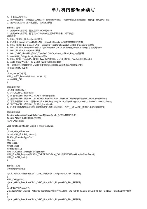
单⽚机内部flash读写1、⾃定义⼯程名称。
2、选择英⽂路径,否则会丢失启动⽂件⽽⽆法编译通过,需要⼿动添加启动⽂件: startup_stm32l431xx.s3、选择MDK-ARM V5开发软件,即KEIL5软件代码编写说明1、按键KEY1按下时,把数据写⼊MCU的flash2、按键KEY2按下时,把写⼊MCU的flash数据并读取出来,打印数据。
调⽤函数:1、HAL_FLASH_Unlock(void);//解锁2、FLASH_EraseInitTypeDef FLASH_EraseInitSturcture;//配置需要擦除的参数3、HAL_FLASHEx_Erase(FLASH_EraseInitTypeDef pEraseInit, uint32_tPageError);//擦除4、HAL_FLASH_Program(uint32_t TypeProgram, uint32_t Address, uint64_t Data);//写数据到flash5、HAL_FLASH_Lock(void);//锁住6、HAL_GPIO_ReadPin(GPIO_TypeDef* GPIOx, uint16_t GPIO_Pin);//检测按键7、void HAL_Delay(uint32_t Delay);//延时8、HAL_GPIO_TogglePin(GPIO_TypeDef* GPIOx, uint16_t GPIO_Pin);//点亮和熄灭LED9、uint8_t OneWord=(__IO uint32_t)addr;//读取地址数据10、printf();//打印数据到串⼝函数需要重新定义函数fputc();才能正常使⽤printf();int fputc(int ch,FILE*f){uint8_t temp[1]={ch};HAL_UART_Transmit(&huart1,temp,1,2);return HAL_OK;}代码编写说明• FLASH读写流程:1、对FLASH写⼊数据流程:1)解锁FLASH:调⽤HAL_FLASH_Unlock(void);2)擦除FLASH:调⽤HAL_FLASHEx_Erase(FLASH_EraseInitTypeDef pEraseInit, uint32_t PageError);3)写⼊数据到FLASH:调⽤HAL_FLASH_Program(uint32_t TypeProgram, uint32_t Address, uint64_t Data);4)锁住FLASH:调⽤HAL_FLASH_Lock(void);2、FLASH读取数据流程直接读取相应的FLASH地址即可:通过(__IO uint32_t)ADDR读取该地址数据代码编写实现#define strLen sizeof(strWriteToFlash1)/sizeof(uint8_t) //写⼊数据的长度#define ADDR 0x0803f800 //写地址写⼊FLASH数据:void writeflash(int addr, uint32_t* writeFlashData){uint32_t PageError = 0;int i=0; HAL_FLASH_Unlock();FLASH_EraseInitTypeDef f;f.Banks=1;f.NbPages=1;f.Page=255;f.TypeErase=0;HAL_FLASHEx_Erase(&f,&PageError);HAL_FLASH_Program(FLASH_TYPEPROGRAM_DOUBLEWORD,addr,writeFlashData[i]);HAL_FLASH_Lock();}代码编写实现while(1)循环内程序:if(HAL_GPIO_ReadPin(KEY1_GPIO_Port,KEY1_Pin)==GPIO_PIN_RESET){HAL_Delay(100);if(HAL_GPIO_ReadPin(KEY1_GPIO_Port,KEY1_Pin)==GPIO_PIN_RESET){printf("KEY1 Press\r\n");writeflash(ADDR,(uint32_t*)&writeFlashData);//擦除并写⼊数据 HAL_GPIO_TogglePin(LED_GPIO_Port,LED_Pin);//LED电平翻转}}if(HAL_GPIO_ReadPin(KEY2_GPIO_Port,KEY2_Pin)==GPIO_PIN_RESET){HAL_Delay(100);if(HAL_GPIO_ReadPin(KEY2_GPIO_Port,KEY2_Pin)==GPIO_PIN_RESET){printf("KEY2 Press\r\n"); ReadFlashData(ADDR,sizeof(writeFlashData),R_OldFlash);//读取写⼊的数据HAL_GPIO_TogglePin(LED_GPIO_Port,LED_Pin); //LED电平翻转 }}```**读取FLASH数据**:`void ReadFlashData(int addr,uint32_t strSize,uint8_t* ReadData){uint8_t OneWord; for(int i=0;i<strSize;i++){OneWord=*(__IO uint32_t*)addr;ReadData[i]=OneWord;addr++;}printf("Read the flash data:>>%s<<,address:%x\r\n",ReadData,addr-strSize);// 显⽰该地址的数据}`**扩展实验**:将移植flash.c,该⽂件有实现写数据到FLASH的多种⽅式,如写字符串数据到 FLASH等。
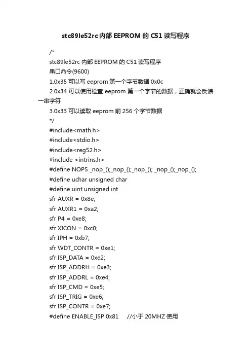
stc89le52rc内部EEPROM的C51读写程序/*stc89le52rc内部EEPROM的C51读写程序串口命令(9600)1.0x35可以写eeprom第一个字节数据0x0c2.0x34可以使用检查eeprom第一个字节的数据,正确就会反馈一串字符3.0x33可以读取eeprom前256个字节数据*/#include<math.h>#include<stdio.h>#include<reg52.h>#include <intrins.h>#define NOP5 _nop_();_nop_();_nop_(); _nop_();_nop_();#define uchar unsigned char#define uint unsigned intsfr AUXR = 0x8e;sfr AUXR1 = 0xa2;sfr P4 = 0xe8;sfr XICON = 0xc0;sfr IPH = 0xb7;sfr WDT_CONTR = 0xe1;sfr ISP_DATA = 0xe2;sfr ISP_ADDRH = 0xe3;sfr ISP_ADDRL = 0xe4;sfr ISP_CMD = 0xe5;sfr ISP_TRIG = 0xe6;sfr ISP_CONTR = 0xe7;#define ENABLE_ISP 0x81 //小于20MHZ使用#define DATA_FLASH_START_ADDR 0x2000//stc89le52rc eeprom起始地址#define TEST_CODE 0x34uchar code start_string[]={"EEPROM first data correct!\n"};uint i=0,k;uchar EEPROM_READ(uint flash_addres);void IAP_disable();void EEPROM_FORMAT(uint flash_addres);void EEPROM_WRITE(uint flash_addres, isp_data);void test_read();void send_byte(uchar bt);void send_string(uchar *ptr, uchar len);void read_string(uint start_addr,uint num);void read_string(uint start_addr, uint num){static uint j,temp;for(j=0;j<num;j++){temp=EEPROM_READ(start_addr+j);NOP5;send_byte(temp);}}void send_string(uchar * ptr, uchar len){static uint j;for(j=0;j<len;j++){send_byte(*(ptr+j));}void send_byte(uchar by){SBUF=by;while(!TI);TI=0;}void IAP_disable(){ISP_CONTR=0;ISP_CMD=0;ISP_TRIG=0;}uchar EEPROM_READ(uint flash_addres) //读取数据{uchar read;ISP_ADDRH=flash_addres>>8;ISP_ADDRL=flash_addres;ISP_CONTR=ENABLE_ISP;ISP_CMD=0x01 ;EA=0;ISP_TRIG=0x46;ISP_TRIG=0xb9 ;NOP5;read=ISP_DATA;IAP_disable();EA=1;return(ISP_DATA);}void EEPROM_WRITE(uint flash_addres,isp_data) //写入数据ISP_ADDRH=flash_addres>>8;ISP_ADDRL=flash_addres;ISP_CONTR=ENABLE_ISP;ISP_CMD=0x02 ;EA=0;ISP_DATA=isp_data;ISP_TRIG=0x46;ISP_TRIG=0xb9;IAP_disable();EA=1;}void EEPROM_FORMAT(uint flash_addres) //擦除{ISP_ADDRH=flash_addres>>8;ISP_ADDRL=flash_addres;ISP_CONTR=ENABLE_ISP;ISP_CMD=0x03;EA=0;ISP_TRIG=0x46;ISP_TRIG=0xb9;IAP_disable();EA=1;}void test_read(){if(RI){RI=0;switch(SBUF)case 0x34:k=EEPROM_READ(DATA_FLASH_START_ADDR);NOP5;if(0x0c==k){send_string(start_string,sizeof(start_string));}send_byte(k);k=0;break;case 0x33:read_string(DATA_FLASH_START_ADDR, 256);break;case 0x35:EEPROM_FORMAT(DATA_FLASH_START_ADDR); //写已经有数据的扇区前要写擦除NOP5;NOP5;NOP5; //可以适当增减延时NOP5;NOP5;NOP5;NOP5;EEPROM_WRITE(DATA_FLASH_START_ADDR,TEST_CODE);//写一个0x0cbreak;default:if(0xff==i)i=0;}k=EEPROM_READ(DATA_FLASH_START_ADDR+(i++)); send_byte(DATA_FLASH_START_ADDR+i);send_byte(k);k=0;break;}}}void init(){TMOD=0x20;SCON=0x50;TL1=0xfd;TH1=0xfd;TR1=1;ET1=1;ES=1;}void main(){init();while(1){test_read();}}。
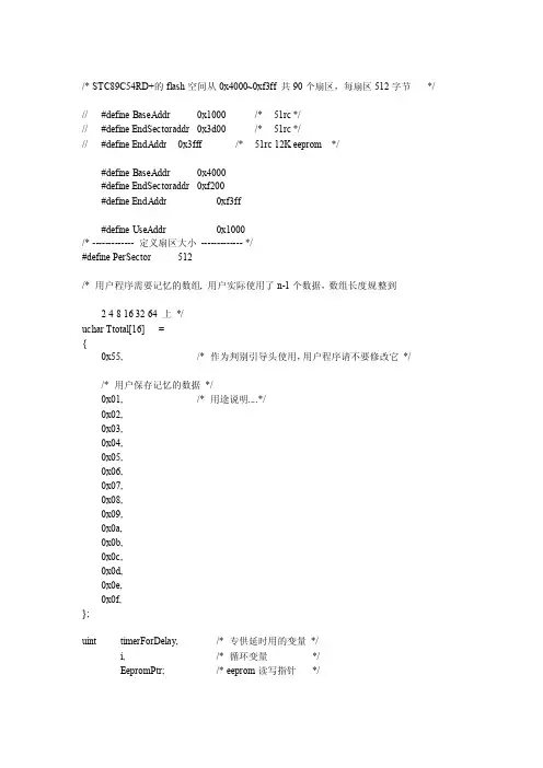
/* STC89C54RD+的flash空间从0x4000~0xf3ff 共90个扇区,每扇区512字节*/// #define BaseAddr 0x1000 /* 51rc */// #define EndSectoraddr 0x3d00 /* 51rc */// #define EndAddr 0x3fff /* 51rc 12K eeprom */#define BaseAddr 0x4000#define EndSectoraddr 0xf200#define EndAddr 0xf3ff#define UseAddr 0x1000/* ------------- 定义扇区大小------------- */#define PerSector 512/* 用户程序需要记忆的数组, 用户实际使用了n-1个数据,数组长度规整到2 4 8 16 32 64 上*/uchar Ttotal[16] ={0x55, /* 作为判别引导头使用,用户程序请不要修改它*//* 用户保存记忆的数据*/0x01, /* 用途说明....*/0x02,0x03,0x04,0x05,0x06,0x07,0x08,0x09,0x0a,0x0b,0x0c,0x0d,0x0e,0x0f,};uint timerForDelay, /* 专供延时用的变量*/i, /* 循环变量*/EepromPtr; /* eeprom读写指针*//* --------------- 命令定义--------------- */#define RdCommand 0x01 /* 字节读*/#define PrgCommand 0x02 /* 字节写*/#define EraseCommand 0x03 /* 扇区擦除*//* 定义常量*/#define Error 1#define Ok 0/* 定义Flash对应于20MHz晶振系统的操作等待时间*//* 时钟倍频时WaitTime用0x00*/#define WaitTime 0x01/* ================ 打开ISP,IAP 功能================= */ void ISP_IAP_enable(void){EA = 0; /* 关中断*/ISP_CONTR = ISP_CONTR & 0x18; /* 0001,1000 */ISP_CONTR = ISP_CONTR | WaitTime; /* 写入硬件延时*/ ISP_CONTR = ISP_CONTR | 0x80; /* ISPEN=1 */ }/* =============== 关闭ISP,IAP 功能================== */ void ISP_IAP_disable(void){ISP_CONTR = ISP_CONTR & 0x7f; /* ISPEN = 0 */ISP_TRIG = 0x00;EA = 1; /* 开中断*/}/* ================ 公用的触发代码==================== */ void ISPgoon(void){ISP_IAP_enable(); /* 打开ISP,IAP 功能*/ISP_TRIG = 0x46; /* 触发ISP_IAP命令字节1 */ ISP_TRIG = 0xb9; /* 触发ISP_IAP命令字节2 */ _nop_();}/* ==================== 字节读======================== */ uchar byte_read(uint byte_addr){ISP_ADDRH = (uchar)(byte_addr >> 8); /* 地址赋值*/ISP_ADDRL = (uchar)(byte_addr & 0x00ff);ISP_CMD = ISP_CMD & 0xf8; /* 清除低3位*/ ISP_CMD = ISP_CMD | RdCommand; /* 写入读命令*/ISPgoon(); /* 触发执行*/ISP_IAP_disable(); /* 关闭ISP,IAP功能*/return (ISP_DA TA); /* 返回读到的数据*/}/* ================== 扇区擦除======================== */ void SectorErase(uint sector_addr){uint iSectorAddr;iSectorAddr = (sector_addr & 0xfe00); /* 取扇区地址*/ISP_ADDRH = (uchar)(iSectorAddr >> 8);ISP_ADDRL = 0x00;ISP_CMD = ISP_CMD & 0xf8; /* 清空低3位*/ ISP_CMD = ISP_CMD | EraseCommand; /* 擦除命令3 */ISPgoon(); /* 触发执行*/ISP_IAP_disable(); /* 关闭ISP,IAP功能*/}/* ==================== 字节写======================== */ void byte_write(uint byte_addr, uchar original_data){ISP_ADDRH = (uchar)(byte_addr >> 8); /* 取地址*/ISP_ADDRL = (uchar)(byte_addr & 0x00ff);ISP_CMD = ISP_CMD & 0xf8; /* 清低3位*/ ISP_CMD = ISP_CMD | PrgCommand; /* 写命令2 */ISP_DA TA = original_data; /* 写入数据准备*/ISPgoon(); /* 触发执行*/ISP_IAP_disable(); /* 关闭IAP功能*/}/* =================== 字节写并校验=================== */ uchar byte_write_verify(uint byte_addr, uchar original_data){ISP_ADDRH = (uchar)(byte_addr >> 8); /* 取地址*/ISP_ADDRL = (uchar)(byte_addr & 0xff);ISP_CMD = ISP_CMD & 0xf8; /* 清低3位*/ISP_CMD = ISP_CMD | PrgCommand; /* 写命令2 */ISP_DA TA = original_data;ISPgoon(); /* 触发执行*//* 开始读,没有在此重复给地址,地址不会被自动改变*/ISP_DA TA = 0x00; /* 清数据传递寄存器*/ISP_CMD = ISP_CMD & 0xf8; /* 清低3位*/ISP_CMD = ISP_CMD | RdCommand; /* 读命令1 */ISP_TRIG = 0x46; /* 触发ISP_IAP命令字节1 */ ISP_TRIG = 0xb9; /* 触发ISP_IAP命令字节2 */_nop_(); /* 延时*/ISP_IAP_disable(); /* 关闭IAP功能*/if(ISP_DA TA == original_data){ /* 读写数据校验*/return Ok; /* 返回校验结果*/ }else{return Error;}}/* ===================== 数组写入===================== */ uchar ArrayWrite(uint begin_addr, uint len, uchar *array){uint i;uint in_addr;/* 判是否是有效范围,此函数不允许跨扇区操作*/if(len > PerSector){return Error;}in_addr = begin_addr & 0x01ff; /* 扇区内偏移量*/if((in_addr + len) > PerSector){return Error;}in_addr = begin_addr;/* 逐个写入并校对*/ISP_IAP_enable(); /* 打开IAP功能*/for(i = 0; i< len; i++){/* 写一个字节*/ISP_ADDRH = (uchar)(in_addr >> 8);ISP_ADDRL = (uchar)(in_addr & 0x00ff);ISP_DA TA= array[i]; /* 取数据*/ISP_CMD = ISP_CMD & 0xf8; /* 清低3位 */ISP_CMD = ISP_CMD | PrgCommand; /* 写命令2 */ISP_TRIG = 0x46; /* 触发ISP_IAP命令字节1 */ISP_TRIG = 0xb9; /* 触发ISP_IAP命令字节2 */_nop_();/* 读回来*/ISP_DA TA = 0x00;ISP_CMD = ISP_CMD & 0xf8; /* 清低3位 */ISP_CMD = ISP_CMD | RdCommand; /* 读命令1 */ISP_TRIG = 0x46; /* 触发ISP_IAP命令字节1 */ISP_TRIG = 0xb9; /* 触发ISP_IAP命令字节2 */_nop_();/* 比较对错*/if(ISP_DA TA != array[i]){ISP_IAP_disable();return Error;}in_addr++; /* 指向下一个字节*/ }ISP_IAP_disable();return Ok;}/* ========================= 扇区读出========================= */ /* 程序对地址没有作有效性判断,请调用方事先保证他在规定范围内*/void ArrayRead(uint begin_addr, uchar len){// uchar xdata data_buffer[]; /* 整个扇区读取缓存区*/ uint iSectorAddr;uint i;iSectorAddr = begin_addr; // & 0xfe00; /* 取扇区地址*/ISP_IAP_enable();for(i = 0; i < len; i++){ISP_ADDRH = (uchar)(iSectorAddr >> 8);ISP_ADDRL = (uchar)(iSectorAddr & 0x00ff);ISP_CMD = ISP_CMD & 0xf8; /* 清低3位 */ISP_CMD = ISP_CMD | RdCommand; /* 读命令1 */ISP_DA TA = 0;ISP_TRIG = 0x46; /* 触发ISP_IAP命令字节1 */ISP_TRIG = 0xb9; /* 触发ISP_IAP命令字节2 */_nop_();Ttotal[i] = ISP_DA TA;iSectorAddr++;}ISP_IAP_disable(); /* 关闭IAP功能*/}/* ==============================================================从eeprom中读取数据============================================================== */void DataRestore(){EepromPtr = BaseAddr; /* 指向eeprom的起始点*/while(EepromPtr < EndAddr) /* 在eeprom的可用区域内 */{if(byte_read(EepromPtr) == 0x55)/* 找到了上一次有效纪录*/{break; /* 寻找完成*/}EepromPtr += 0x10; /* 指向下一个小区*/ }if(EepromPtr >= EndAddr) /* 如果照遍都没有,是新片*/{EepromPtr = BaseAddr; /* 指向eeprom的起始点*/for(i=0;i<90;i++){SectorErase(EepromPtr+0x200*i); /* 全部扇区擦除*/}while(ArrayWrite(EepromPtr, 0x10, Ttotal)) /* 写默认值*/{ /* 写入失败才运行的部分*/byte_write(EepromPtr, 0); /* 该单元已经失效*/if(EepromPtr < EndAddr){EepromPtr += 0x10; /* 换一块新的小区*/}else{P1=0; /* 指示芯片内eeprom全坏 */EA= 0; /* 不再做任何事*/while(1); /* 死机*/}}}ArrayRead(EepromPtr, 16);}/* ==============================================================将需要记忆的数据保存到eeprom============================================================== */void DataSave(){uint wrPtr; /* 临时指针*/ NextArea:byte_write_verify(EepromPtr, 0); /* 将原来的标记清除*/wrPtr = EepromPtr & 0xfe00; /* 上一个扇区的起始地址*/EepromPtr += 0x10; /* 目标存入地址*//* ------------------ 判断是否启用新的扇区---------------- */if((EepromPtr & 0x1ff)==0){SectorErase(wrPtr); /* 将上一个扇区擦除,备用*/if(EepromPtr>=EndAddr) /* 已经用完了最后一个区域*/{EepromPtr = BaseAddr; /* 从头开始*/}}/* -------------------- 数据存入前的准备------------------ *//* 。


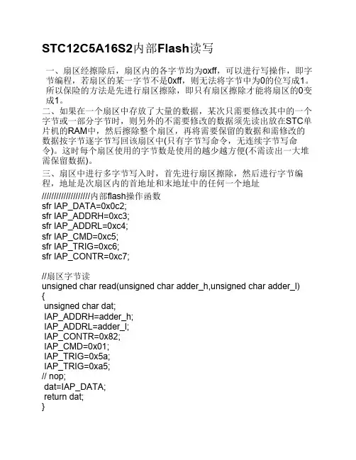
STC12C5A16S2内部Flash读写一、扇区经擦除后,扇区内的各字节均为oxff,可以进行写操作,即字节编程,若扇区的某一字节不是0xff,则无法将字节中为0的位写成1。
所以保险的方法是先进行扇区擦除,即只有扇区擦除才能将扇区的0变成1。
二、如果在一个扇区中存放了大量的数据,某次只需要修改其中的一个字节或一部分字节时,则另外的不需要修改的数据须先读出放在STC单片机的RAM中,然后擦除整个扇区,再将需要保留的数据和需修改的数据按字节逐字节写回该扇区中(只有字节写命令,无连续字节写命令)。
这时每个扇区使用的字节数是使用的越少越方便(不需读出一大堆需保留数据)。
三、扇区中进行多字节写入时,首先进行扇区擦除,然后进行字节编程,地址是次扇区内的首地址和末地址中的任何一个地址////////////////////内部flash操作函数sfr IAP_DATA=0x0c2;sfr IAP_ADDRH=0xc3;sfr IAP_ADDRL=0xc4;sfr IAP_CMD=0xc5;sfr IAP_TRIG=0xc6;sfr IAP_CONTR=0xc7;//扇区字节读unsigned char read(unsigned char adder_h,unsigned char adder_l){unsigned char dat;IAP_ADDRH=adder_h;IAP_ADDRL=adder_l;IAP_CONTR=0x82;IAP_CMD=0x01;IAP_TRIG=0x5a;IAP_TRIG=0xa5;// nop;dat=IAP_DATA;return dat;}//扇区字节写void write(unsigned char adder_h,unsigned char adder_l,unsigned char dat){IAP_DATA=dat;IAP_ADDRH=adder_h;IAP_ADDRL=adder_l;IAP_CONTR=0x82;IAP_CMD=0x02;IAP_TRIG=0x5a;IAP_TRIG=0xa5;// nop;}void del(unsigned char adder_h,unsigned char adder_l){IAP_ADDRH=adder_h;IAP_ADDRL=adder_l;IAP_CONTR=0x82;IAP_CMD=0x03;IAP_TRIG=0x5a;IAP_TRIG=0xa5;}//把设置的闹钟值存进单片机内部flash函数void restore(unsigned char hour,unsigned char min){del(0x00,0x00);//将扇区内的每个字节都变成0xffdelay_5ms();write(0x00,0x00,hour);//第一个扇区的第一个地址存放设置的小时值 delay_5ms();write(0x02,0x00,min);//第二个扇区的第一个地址存放设置的fen值}。
STC单片机烧写程序使用教程烧写程序是将程序代码写入至单片机中的一项重要工作。
本教程将分为以下几个步骤来介绍STC单片机烧写程序的具体操作:1.准备工作:在开始烧写程序之前,需要准备以下材料和设备:-STC单片机烧录器:常用的有STC-ISP、STC-USB等多种类型;-硬件电路:包括电源、晶振、电容等;- STC单片机开发工具:如Keil C、IAR等;-STC单片机程序代码。
2.连接电路:首先,需要将STC单片机烧录器与电路板连接。
将烧录器接口插到电脑的USB接口上,再选择合适的接口线连接烧录器与电路板,一般是通过芯片上的10针扎线连接。
3.安装驱动程序:在连接好电路后,需要先安装USB烧录器驱动程序,驱动程序一般会附带在设备的光盘中,在安装完成后,电脑就可以识别到烧录器设备了。
4.打开烧录软件:将烧录器连接到电脑后,需要打开STC单片机烧录软件。
根据你所使用的烧录器型号来确定使用何种软件,比如STC-ISP、STC-USB等。
打开软件后,可以看到一些操作选项。
5.选取单片机型号:在烧录软件中,需要选择要烧录的单片机型号。
一般来说,不同的单片机型号对应不同的程序代码和芯片参数,因此需要确保选择正确的单片机型号。
6.导入程序代码:将准备好的程序代码导入烧录软件。
一般来说,程序代码是以.c 或.hex文件的形式保存的,你可以通过打开文件的方式将其导入烧录软件。
7.设置烧写方式:在烧录软件中,需要设置烧写方式。
通常有两种选择:ISP(串行编程)和ICP(并行编程),其中ISP方式较为常用。
选择适合的烧写方式后,可以设置烧写速度、读出校验等参数。
8.擦除单片机:在烧写程序之前,需要先将单片机中原有的程序代码擦除。
擦除操作会将单片机中的所有数据清零,为接下来的烧写作准备。
大多数烧录软件会有一个擦除或清零的选项,点击后即可开始擦除。
9.烧写程序:擦除完成后,即可开始烧写程序。
点击“开始”或“烧写”按钮,烧录软件会根据设置的参数将程序代码写入到单片机中。
STC单片机烧写程序使用教程
1、把开发板连接到电脑上
把串口线(每端9个孔的线)一端插到电脑的串口上,一端插在开发板上;把USB一端插到电脑的串口上,一端(圆头)插在开发板上, (都是傻瓜式的接口,我相信哥们不会插错吧.如果你插不上,就不要用力,以免插错损坏接口,建议你找个对电脑硬件熟悉的哥们帮忙,呵呵~~),这时开发板上电源指示灯DS9亮。
2、找到烧写软件如图-1
图-1
3、鼠标左键单击 STC_ISP_V3.1 打开如图-2 界面
图-2
4、选择正确的单片机型号(单片机上的第一行字既是型号), 鼠标
左键单击下拉箭头界面如图-3
图-3
5、鼠标左键单击所用的型号,我用的是STC89C52RC单片机,所以
选择后的界面如图-4
图-4
6、选择我需要烧写到单片机里的程序
鼠标左键单击出现图-5 界面
图-5
找到我们需要烧写的文件,然后鼠标左键双击文件就行(如图-5的lighten_LED)
7、选择串口
鼠标左键单击下拉箭头,选择和单片机相连接的电脑串口如图-6
图-6
8、鼠标左键点击开始下载程序,要确保此前开发
板电源没有打开,即串口旁的CP发光二极管不亮;如果串口旁的CP发光二极管亮,按一下发光二极管DS9旁边的蓝色电源按钮断电。
9、按一下开发板发光二极管DS9旁边的蓝色电源按钮给单片机上
电。
10、下载成功后出现如图-7界面(注意红圈内的内容)
图-7
11、下载完成我们就可以看到程序运行的结果了,这时你可能很兴
奋,可能很郁闷.兴奋因为单片机按照你的想法干事了;郁闷是因为单片机不按你想的做事,那恭喜你,继续奋战吧~~~~~~__。
Programming Atmel’s AT29 Flash FamilyIntroductionAtmel offers a diverse family of smallsector Flash memory devices ranging indensity from 256K to 4M bits. These de-vices read and program with a singlevoltage supply. The nominal supply volt-age is 5V for the AT29CXXX, 3.3V forthe “low voltage” AT29LVXXX, and 3Vfor the “Battery Voltage” AT29BVXXXFlash memory family. The entire FlashPEROM product line is designed to al-low users to have one common pro-gramming algorithm for all three Flashvoltage families. Therefore, upgradingfrom one density to another and from ahigher voltage to a lower voltage deviceis simplified.This application note describes the de-sign benefits of Atmel’s AT29 Flash ar-chitecture as well as how the device IDfeature is used to adjust for varying den-sities and supply voltages. In addition,Atmel’s Software Data Protection (SDP)feature, which prevents inadvertentwrites, is described. An example is givento illustrate the ease with which the pro-gramming software can be written to ac-commodate four different 4M bit Flashdevices: the AT29C040, theAT29LV040, and the newer generationFlash devices, the AT29C040A and theAT29LV040A.Hardware and software has been devel-oped to demonstrate the relevant designissues. The demo uses an AT89C51Flash-based microcontroller (which hasthe same pinout and instruction set asan 80C51) as the host processor and a“C” language program for the software.The software automatically adjusts theamount of time required for program-ming the varying voltage versions of the4M bit Flash devices in addition to ac-commodating for their different sectorsizes.The AT89C51, a member of Atmel’sgrowing family of Flash microcontrollerdevices, features 4K bytes of in-systemreprogrammable Flash memory (see At-mel application note “AT89C51 In-Cir-cuit Programming” for additional infor-mation). Current and future versions ofAtmel’s microcontroller family incorpo-rate from as little as 1K byte of Flashmemory to as much as 128K bytes, pro-viding many density options for differentapplications. Other versions will also in-clude special architectures such as acombination of Flash and parallelE2PROM memory on board.Programming Flash DevicesUnlike Atmel’s Flash memories, pre-vious generations of Flash memorieshad large sectors, typically 4K to 128Kbytes, and required that an entire sectorbe erased prior to programming. Gener-ally, the sector erase cycle time washundreds or thousands of millisecondsand could be as long as 30 seconds forthe entire memory array. In addition, aseparate high voltage supply was re-quired for a write and erase operation. At-mel’s AT29 Flash memory family has sim-plified usage by having only one supplyvoltage, reducing the sector size, havingthe programming similar to an SRAMwrite operation, and decreasing signifi-cantly the total programming time.Small sector sizes reduce the amount ofsystem resources necessary for pro-gramming. When only a few bytes in aFlash memory need to be altered, aRAM image of the Flash sector must becreated. The RAM must then be alteredwith the new data, and the image trans-Flash4-251cause Atmel’s Flash devices have small sector sizes (from 64- to 512-bytes, depending on the memory density), the RAM requirements are much less than those of large sec-tor Flash devices. Often, the system RAM available is suf-ficient for Atmel’s Flash, whereas large sector Flash de-vices usually require an additional SRAM.A second advantage of Atmel’s AT29 Flash is that an en-tire sector can be updated during a single program opera-tion, instead of the byte-by-byte programming of previous generation Flash memories. This saves significant pro-gramming time when updating an entire sector, especially when comparing Atmel’s small sector devices with large sector devices. In addition, Atmel’s devices do not require a sector erase prior to writing, thus saving additional pro-gramming time. The maximum sector program time is 10msec for the AT29CXXX family and 20 msec for the AT29LVXXX/AT29BVXXX families.AT29C040 and AT29C040A ArchitectureThe AT29C040 provides operation similar to a byte-wide SRAM. The device has eight data lines and 19 address lines. The familiar three input control lines are also pre-sent (CE, OE, WE). Read operations are identical to an SRAM, but write operations are somewhat different due to the write cycle time (t WC ) requirements of all Flash memo-ries. Flash write operations take several milliseconds to complete, compared to the nanosecond writes of SRAM devices. It should be noted that Atmel’s AT29 Flash PEROMs require only a write operation; the erase opera-tion is automatically performed internally in the device.Data is loaded into the AT29C040 one sector at a time,with each sector consisting of 512-bytes. The sector cho-sen for modification is defined by the upper order address bits (A9-A18). The entire sector must be loaded during the write operation. Any byte not loaded during the sector load will contain FF (hex) after the write operation has completed. Address lines A0 through A8 define the loca-tion of the bytes within a sector. All data must be loaded into the same sector (A9 through A18 must remain con-stant) and can be randomly loaded within that sector.The AT29C040A is identical to the AT29C040 except for the sector size and the Device ID Code (the Device ID Code is described later). The AT29C040A has a 256-byte sector (instead of a 512-byte sector) which is defined by address lines A8 through A18; the bytes within the sector are determined by address lines A0 through A7.Software Data Protection (SDP)One concern of systems designers when using nonvolatile programmable memories is the possibility of inadvertent write operations that can be caused by noise or by power-up and power-down sequences. Atmel’s Flash memories provide a feature called Software Data Protection (SDP)that addresses this issue. The user can enable SDP upon receipt of the device from Atmel, and its usage is highly recommended. Data can be written into a sector with or without SDP enabled. However, once SDP has been en-abled, the device requires that all subsequent write opera-tions perform a series of “dummy” write operations before loading the chosen sector with data. The “dummy” writes consist of loading three known data values into three pre-defined addresses. This 3-byte sequence preceding a write operation virtually eliminates the chance of inadver-tent write operations. The sequence is described below.1.Load Data AA (hex) into Address 05555 (hex)2.Load Data 55 into Address 02AAA 3.Load Data A0 into Address 055554.Load desired sector with data5.Pause t WC (device write cycle time)6.Continue with next operation.If SDP is enabled, any attempt to write to the device with-out the 3-byte command sequence will start a write cycle.However, no data will actually be written to the device, and during this “write” cycle time (t WC ), valid data cannot be read from the Flash.Product and Manufacturer IDAtmel’s Flash memory devices allow the user to access both device and manufacturer information. This feature al-lows a system to determine exactly which Flash memory is being used. Once this is known, the host system can choose different algorithms for write operations in order to accommodate for differences in device density, V CC re-quirements, sector size, and required write cycle time.Product and manufacturer ID information is determined with the Software Product Identification procedure, which is similar to the Software Data Protection sequence. The sequence is described below.1.Load Data AA (hex) into Address 05555 (hex)2.Load Data 55 into Address 02AAA3.Load Data 90 into Address 055554.Pause t WC (device write cycle time)5.Read Address 00000Data read is the Manufacturer Code 6.Read Address 00001Data read is the Device ID Code 7.Load Data AA into Address 055558.Load Data 55 into Address 02AAA 9.Load Data F0 into Address 0555510.Pause t WC (device write cycle time)4-252Flashto illustrate the pertinent device information that can be determined once the Device ID Code is known. Please refer to the table at the end of this application note for in-formation on other Flash devices.Programming DemonstrationHardware and software descriptions have been prepared to demonstrate how Atmel’s AT29 Flash memories can be reprogrammed. The descriptions are provided in the fol-lowing two sections. A circuit schematic of the demonstra-tion hardware and a source code listing of the software are also included.Hardware DescriptionThe demo hardware consists of a 12 MHz AT89C51Flash-based microcontroller with 4K bytes of on-board Flash memory. The internal AT89C51 Flash memory is used for boot code, and the external 8K x 8 SRAM and the AT29C040A are mapped as data memory. The AT29C040A is also mapped as program memory to facili-tate off-chip program execution. The AT89C51 can only access a maximum of 64K bytes of data memory space,while the AT29C040A has 512K bytes of storage capacity.To solve this size mismatch, the AT29C040A is bank switched into the AT89C51 data memory map in 8K byte blocks. The bank switching is performed with six general purpose I/O port bits on the AT89C51. The system ad-dress map is shown below.System Address MapAT89C51Microcontroller 0000-1FFFInternal program memory 8K x 8 Static RAM 2000-3FFF Data memory AT29C040A Flash4000-5FFFProgram and data memorySoftware DescriptionThe software demonstrates how the Device ID Code can be used to allow a single program to work with different Atmel Flash memories. The program uses Atmel’s 4M bit Flash (AT29C040, AT29LV040, AT29C040A, and AT29LV040A) as an example, but the software can be easily adapted to accommodate other device densities.In order to program the Flash memory, the software must first determine which Flash device is being used. This is accomplished by first putting the device into the Software Product Identification mode (described in the “Product and Manufacturer ID” section of this application note). The pro-gram subsequently reads the Device ID Code and exe-cutes the 3-byte command sequence to return the Flash to the standard operating mode. Using the Device ID Code,the program then determines the appropriate sector size and write cycle time (t WC ) for the particular 4M bit Flash being used.To demonstrate a sector write, the program proceeds to load the SRAM with “dummy” data. After the data has been loaded, the program transfers the data from the SRAM to a predefined sector (within one of the mapped 8K byte blocks) of the 4M bit Flash. After pausing the re-quired write cycle time (t WC ), the sector that was just writ-ten is transferred back to the SRAM buffer.SummaryAtmel’s AT29 Flash memories are designed to allow all densities and device configurations to be programmed us-ing the same programming algorithm. The user has to sim-ply determine the Device ID Code and set the appropriate sector size and write cycle time. This operation need only be performed once provided the sector size and write cy-cle information is saved. If only one density or configura-tion will ever be used, then reading of the Device ID Code can be eliminated, and the sector size and write cycle in-formation can be predefined in the software. The table at the end of this application note details the device informa-tion and the Device ID Codes for Atmel’s AT29XXX Series of Flash PEROMs.As demonstrated, programming Atmel’s AT29 Flash is a simple process, similar to loading an SRAM. Architectural and circuit features within the devices minimize software and system overhead while simplifying programming pro-cedures. Atmel’s AT29 Flash memories require only about one-tenth of the typical software, buffer memory,and performance overhead of previous generation Flash, thus providing substantial system cost savings.Flash4-253Atmel AT29 Flash Memories4-254Flash/*****************************************************************/ /* This program demonstrates how a sector in one of the 512K X 8 *//* variants can be programmed. The program first determines *//* exactly which device is available by reading the device ID. *//* A sector is then programed with data that is copied from an *//* SRAM buffer. After waiting for the programming cycle to *//* complete the data is copied back from the 29C040 to the SRAM *//* buffer. *//* *//* The sector size and programming time are determined *//* by examining the device ID. The different 512K X 8 devices *//* have either a 256- or 512-byte sector size and a 10 mS or 20 *//* mS tWC. *//*****************************************************************//***********************//* COMPILER DIRECTIVES *//***********************/ .asm.linklist .symbols .endasm#include “c8051sr.h”/********************//* GLOBAL VARIABLES *//********************/unsigned char part_id; /* DEVICE ID VALUE */int sector_size; /* DEVICE SECTOR SIZE */int twc; /* DEVICE PROGRAMMING TIME REQUIRED */unsigned char data_buffer[512]; /* SRAM DATA BUFFER */unsigned char block_number; /* WHICH BLOCK TO PROGRAM */unsigned int sector_address; /* ADDRESS WITHIN SECTOR TO PROGRAM */unsigned int address_pointer; /* SCRATCH PAD ADDRESS REGISTER */unsigned char temp_byte; /* SCRATCH PAD DATA REGISTER *//***********************//* SUPPORT SUBROUTINES *//***********************//********************************************************************//* DELAYMS performs a time delay. The variable ticks indicates the *//* length of the delay in mS. This routine is dependant upon the *//* clock rate of the 89C51. If a clock rate other than 12 MHz is *//* used the variable ’count’ must be modified. *//********************************************************************/void delayms(char ticks){char count;for (ticks = ticks; ticks >= 0; ticks—) {for (count = 0; count <= 13; count++){Flash4-255}}}/*****************************************************************//* ENTER_ID_MODE is used to put the 29C040 into Software Product *//* Identification mode. The three step sequence is performed in *//* assembly because of tBLC requirements of the 29C040. *//*****************************************************************/void enter_id_mode(){.asmmov a,#05hmov p1,amov dptr,#4555hmov a,#aahmovx @dptr,a ;write AAh to address 05555hmov a,#02hmov p1,amov dptr,#4aaahmov a,#55hmovx @dptr,a ;write 55h to address 02AAAhmov a,#05hmov p1,amov dptr,#4555hmov a,#90hmovx @dptr,a ;write 90h to address 05555h.endasm}/********************************************************************/ /* LEAVE_ID_MODE is used to remove the 29C040 from Software Product */ /* Identification mode. The three step sequence is performed in */ /* assembly because of tBLC requirements of the 29C040. */ /********************************************************************/void leave_id_mode(){.asmmov a,#05hmov p1,amov dptr,#4555hmov a,#aahmovx @dptr,a ;write AAh to address 05555hmov a,#02hmov p1,amov dptr,#4aaahmov a,#55hmovx @dptr,a ;write 55h to address 02AAAhmov a,#05hmov p1,amov dptr,#4555hmov a,#f0h4-256Flashmovx @dptr,a ;write F0h to address 05555h .endasm }/*********************************************************************//* GET_ID is used read the value at location 00001 of the 20C040. *//* The value read from the device is returned to the calling routine *//*********************************************************************/unsigned char get_id(){P1 = 0x00; /* read from block 00h */ .asmmov dptr,#4001h ;read from address 00001h movx a,@dptr ; (flash offset = 4000h) .endasmreturn(A); /* return data value */}/******************************************************************//* GET_PART_ID determines the device ID of the 29C040 being used. *//* The ID value is returned to the calling routine *//******************************************************************/unsigned char get_part_id(){unsigned char part_id;enter_id_mode(); /* enter Identification mode */ delayms(20); /* delay 20mS */part_id = get_id(); /* read device ID from address 1 */ leave_id_mode(); /* exit from Identification mode */ delayms(20); /* delay 20mS */return(part_id); /* return device ID value */}/*****************************************************************//* SET_PARAMETERS is used to define what sector size and write *//* cycle is required for the particular 29C040 being used *//* The sector size is stored in the global variable SECTOR_SIZE, *//* and the programming time is stored in the global variable TWC.*//*****************************************************************/void set_parameters(unsigned char part_id){switch(part_id) {case 0x5b : sector_size = 512; /* is the device a 29C040 */ twc = 10; break;case 0xa4 : sector_size = 256; /* is the device a 29C040A */ twc = 10; break;case 0x3b : sector_size = 512; /* is the device a 29LV040 */ twc = 20;break;Flash4-257case 0xc4 : sector_size = 256; /* is the device a 29LV040A */ twc = 20;break;default : sector_size = 0; /* variables default to 0 */twc = 0;}}/*****************************************************************//* DUMMY_BUFFER_LOAD simply loads the SRAM buffer with the value *//* passed in IN_VALUE. Although the SRAM buffer has 512-bytes, *//* only the number of bytes required to fill a sector are loaded.*//*****************************************************************/ void dummy_buffer_load(char in_value){int count;for (count = 0; count <= sector_size; count++){data_buffer[count] = in_value;}}/*****************************************************************//* WRITE_SECTOR copies data from the SRAM buffer into the sector *//* specified in the 29C040. After loading the sector the routine*//* paused the required tWC for the programming cycle to complete.*//*****************************************************************/ void write_sector(){.asmmov a,#05h ;perform 3 step SDP sequencemov p1,amov dptr,#4555hmov a,#aahmovx @dptr,a ;write AAh to address 05555hmov a,#02hmov p1,amov dptr,#4aaahmov a,#55hmovx @dptr,a ;write 55h to address 02AAAhmov a,#05hmov p1,amov dptr,#4555hmov a,#A0hmovx @dptr,a ;write A0h to address 05555hmov dptr,#_block_numbermovx a,@dptrmov P1,a ;set up block addressmov dptr,#_sector_size ;load sector sizemovx a,@dptrmov r0,ainc dptrmovx a,@dptrmov r1,a4-258Flashmov dptr,#_sector_address ;load first sector address to write movx a,@dptr add a,#40h mov r3,a inc dptr movx a,@dptr mov r2,amov dptr,#_data_buffer ;load pointer to data_buffer nextwr: movx a,@dptr ;load data to write to 29C040 inc dptr ;increment data_buffer pointer push dpl push dph mov dpl,r2 mov dph,r3movx @dptr,a ;write data to 29C040inc dptr ;increment flash address pointer mov r2,dpl mov r3,dph pop dph pop dpldjnz r1,nextwr ;decrement byte counterdjnz r0,nextwr ; loop until sector has been loaded .endasmdelayms(twc); /* delay for the programming cycle */}/********************************************************************//* READ_SECTOR copies a sector from the 29C040 into the SRAM buffer *//* Either 256- or 512-bytes are transfered depending on the size of *//* the sector. *//********************************************************************/void read_sector(){unsigned int count;P1 = block_number; /* initial block # */ address_pointer = sector_address + 0x4000; /*create address pointer*/ for (count = 0; count < sector_size; count++) /*transfer sector to SRAM*/ {.asmmov dptr,#_address_pointer ;load address pointer’s addressmovx a,@dptr ;load address pointer high bytemov b,a inc dptrmovx a,@dptr ;load address pointer low byte mov dpl,a mov dph,bmovx a,@dptr ;read data from 29C040 mov dptr,#_temp_bytemovx @dptr,a ;store data from 29C040 into temp_byte .endasmdata_buffer[count] = temp_byte; /*place data into SRAM*/address_pointer = address_pointer + 1; /*increment address pointer*/ }}/************/Flash4-259/* MAINLINE *//************/main(){part_id = get_part_id(); /* GET PART ID */set_parameters(part_id); /* DETERMINE WRITE PARAMETERS */dummy_buffer_load(0x55); /* LOAD SRAM BUFFER WITH DUMMY DATA */ block_number = 0x1f; /* SPECIFY BLOCK NUMBER TO WRITE */sector_address = 0x0400; /* SPECIFY ADDRESS WITHIN BLOCK */write_sector(); /* COPY SRAM BUFFER TO 29C040 */read_sector(); /* COPY 29C040 SECTOR TO SRAM */}4-260FlashFlash4-261。
STC单片机内部FLASH读写程序(http://control.blog.sina。
com。
cn/admin/ar ticle/article_add.php)电子伙伴发表于 2006—4-11 16:26:001推荐//#i nclude "STC89C51.h”//#i nclude 〈intrins。
h〉#define ERROR 0#define OK 1#define WAIT_TIME 0x00 //mcu clock 40mhz//#define WAIT_TIME 0x01 //mcu clock 20mhz//#define WAIT_TIME 0x02 //mcu clock 10mhz//#define WAIT_TIME 0x03 //mcu clock 5mhz#define HOUR 0x8000#define MINUTE 0x8001void ISP_EN(void){EA = 0;// 关中断ISP_CONTR = ISP_CONTR & 0x18;// 0001,1000ISP_CONTR = ISP_CONTR | WAIT_TIME;ISP_CONTR = ISP_CONTR | 0x80; // 1000,0000}void ISP_DI(void){ISP_CONTR = ISP_CONTR & 0x7f;// 0111,1111ISP_TRIG = 0x00;EA = 1;// 开中断}unsigned char Byte_read(unsigned int byte_addr){ISP_ADDRH = (unsigned char)(byte_addr 〉> 8);ISP_ADDRL = (unsigned char)(byte_addr & 0x00ff);ISP_CMD = ISP_CMD & 0xf8;// 1111,1000ISP_CMD = ISP_CMD | 0x01;// 0000,0001 字节读数据存储区ISP_EN();ISP_TRIG = 0x46;ISP_TRIG = 0xb9;_nop_();ISP_DI();return (ISP_DATA);}void Sector_erase(unsigned int Sector_addr){unsigned char addre;addre = (unsigned char)(Sector_addr >> 8); // 1111,1110,0000,0000; 取扇区地址ISP_ADDRH = addre&0xfe;ISP_ADDRL = 0x00;ISP_CMD = ISP_CMD &0xf8;// 1111,1000ISP_CMD = ISP_CMD | 0x03; // 0000,0011 扇区擦除数据存储区ISP_EN();ISP_TRIG = 0x46; // 触发ISP_IAP命令ISP_TRIG = 0xb9;// 触发ISP_IAP命令_nop_();ISP_DI();}void Byte_program(unsigned int byte_addr, unsigned char DataBuf){ISP_ADDRH = (unsigned char)(byte_addr 〉〉 8);ISP_ADDRL = (unsigned char)(byte_addr & 0x00ff);ISP_CMD = ISP_CMD &0xf8; // 1111,1000ISP_CMD = ISP_CMD |0x02;// 0000,0010 字节编程数据存储区ISP_DATA = DataBuf;ISP_EN();ISP_TRIG = 0x46; // 触发ISP_IAP命令ISP_TRIG = 0xb9; // 触发ISP_IAP命令_nop_();ISP_DI();}unsigned char ByteProgramVerify(unsigned int byte_addr, unsigned char DataBuf){ISP_ADDRH = (unsigned char)(byte_addr 〉> 8);ISP_ADDRL = (unsigned char)(byte_addr & 0x00ff);ISP_CMD = ISP_CMD & 0xf8;// 1111,1000ISP_CMD = ISP_CMD |0x02;// 0000,0010 字节编程数据存储区ISP_DATA = DataBuf;ISP_EN();ISP_TRIG = 0x46;ISP_TRIG = 0xb9;_nop_();ISP_DATA = 0x00;ISP_CMD = ISP_CMD & 0xf8; // 1111,1000ISP_CMD = ISP_CMD | 0x01;// 0000,0001ISP_TRIG = 0x46; // 触发ISP_IAP命令ISP_TRIG = 0xb9;// 触发ISP_IAP命令_nop_();ISP_DI();if(ISP_DATA==DataBuf)return OK;else return ERROR;}。
STC单片机EEPROM的读写程序汇编语言写的,依据stc单片机官方提供的资料,测试ok,另外还有c语言的大家可到论坛去找。
stc的eeprom 功能还是不错的,可以简化我们的外围电路,但是缺点是是有就那就是写入速度太慢了,只能按扇区的写,不能字节写.下面是代码AUXR1 EQU 0A2HISPDATA EQU 0E2HISPADDRH EQU 0E3HISPADDRL EQU 0E4HISPCMD EQU 0E5HISPTRIG EQU 0E6HISPCONTR EQU 0E7HORG 0000HAJMP MAINORG 0030HMAIN:MOV AUXR1,#0INC AUXR1MOV DPTR,#2000H ACALL ERASEMOV A,#0FEH ACALL EEPROMW ACALL EEPROMR INC AUXR1AJMP MAIN ERASE:;擦除MOV ISPCONTR,#81H MOV ISPCMD,#03H MOV ISPADDRH,DPH MOV ISPADDRL,DPL CLR EAMOV ISPTRIG,#46H MOV ISPTRIG,#0B9H NOPSETB EAACALL ISPXXRET EEPROMW:;写MOV ISPCONTR,#81H MOV ISPCMD,#02HMOV ISPADDRH,DPH MOV ISPADDRL,DPL MOV ISPDATA,A CLR EAMOV ISPTRIG,#46H MOV ISPTRIG,#0B9H NOPSETB EAACALL ISPXXRET EEPROMR:;读MOV ISPCONTR,#81H MOV ISPCMD,#01H MOV ISPADDRH,DPH MOV ISPADDRL,DPL CLR EAMOV ISPTRIG,#46H MOV ISPTRIG,#0B9H NOPMOV A,ISPDATA SETB EAACALL ISPXXRETISPXX:MOV ISPCONTR,#0 MOV ISPCMD,#0 MOV ISPTRIG,#0 RETDEL:MOV R2,#0FFHD1:MOV R1,#0FFH DJNZ R1,$DJNZ R2,D1RETEND。
一、Flash块结构说明我们所用板子上flash一共划分了259个块,0-254块为128kByte,255-258块为32kByte。
各个块的地址范围如下图:我们要读flash中某个地址的数据,只要发送相关命令即可,下面会详细说明。
向flash 中写数据较复杂,首先必须将目标地址所属块解锁,然后擦除,最后才能写数据,只要解锁与擦除后就可连续往flash中写,但是不能向同一个地址写,这样会写不进去。
以上的解锁与擦除是针对一个块的操作,是将地址所属块全部擦除,写程序的时候注意不要误擦其它块。
写过程详细步骤见(二)。
二、通过c对Flash进行读写操作说明通过高级语言(如c)对flash进行读写,我们开始的想法是自己做一个flash读写的IP 核,然后在c中调用此ip核来实现对flash的读写,但是这种做法比较复杂,一直进展不顺利。
后来一次偶然的试验发现直接向总线写读写flash的命令即可对flash进行读写,也就是说直接将以前在verilog中读写falsh的操作过程搬到c语言中,这大大降低了c中读写flash 的难度。
具体说明如下:1.读flash读取flash包括两个步骤:1,首先向目标地址写x00ff,告诉flash表示要读数据了。
2,通过XIo_In16函数读取目标地址的数据。
下面两行代码即可读取flash中地址为dataAddr的数据,保存在value中。
XIo_Out16(FlashBaseAddr+2*dataAddr,0x00ff);u16 value = XIo_In16(FlashBaseAddr+2*dataAddr);其中FlashBaseAddr为flash在硬件设计中分配的基地址,并且读取的数据只能是16位的数据,这是因为flash的数据输入输出出引脚只有16位。
2.写flash向falsh中写数据包括三个步骤:1,对目标地址所属块进行解锁操作(write0x60,write 0xD0);2,擦除目标地址所属块(write 0x20,write 0xD0);3,读取寄存器状态((write0x70,read regstatu)),当寄存器状态值为0x80说明准备就绪,可以下一个操作;4,向目标地址写数据(write 0x0040,write data),data为你要写如flash的数据。
STC单片机内部FLASH读写程序(/admin/article/article_a dd.php)
电子伙伴发表于 2006-4-11 16:26:00
1
推荐
//#i nclude "STC89C51.h"
//#i nclude <intrins.h>
#define ERROR 0
#define OK 1
#define WAIT_TIME 0x00 //mcu clock 40mhz
//#define WAIT_TIME 0x01 //mcu clock 20mhz
//#define WAIT_TIME 0x02 //mcu clock 10mhz
//#define WAIT_TIME 0x03 //mcu clock 5mhz
#define HOUR 0x8000
#define MINUTE 0x8001
void ISP_EN(void)
{
EA = 0; // 关中断
ISP_CONTR = ISP_CONTR & 0x18; // 0001,1000
ISP_CONTR = ISP_CONTR | WAIT_TIME;
ISP_CONTR = ISP_CONTR | 0x80; // 1000,0000
}
void ISP_DI(void)
{
ISP_CONTR = ISP_CONTR & 0x7f; // 0111,1111
ISP_TRIG = 0x00;
EA = 1; // 开中断}
unsigned char Byte_read(unsigned int byte_addr)
{
ISP_ADDRH = (unsigned char)(byte_addr >> 8);
ISP_ADDRL = (unsigned char)(byte_addr & 0x00ff);
ISP_CMD = ISP_CMD & 0xf8; // 1111,1000 ISP_CMD = ISP_CMD | 0x01; //
0000,0001 字节读数据存储区
ISP_EN();
ISP_TRIG = 0x46;
ISP_TRIG = 0xb9;
_nop_();
ISP_DI();
return (ISP_DATA);
}
void Sector_erase(unsigned int Sector_addr)
{
unsigned char addre;
addre = (unsigned char)(Sector_addr >> 8); //
1111,1110,0000,0000; 取扇区地址
ISP_ADDRH = addre&0xfe;
ISP_ADDRL = 0x00;
ISP_CMD = ISP_CMD & 0xf8; // 1111,1000
ISP_CMD = ISP_CMD | 0x03; // 0000,0011 扇区擦除数据存储区
ISP_EN();
ISP_TRIG = 0x46; // 触发ISP_IAP命令ISP_TRIG = 0xb9; // 触发ISP_IAP命令 _nop_();
ISP_DI();
}
void Byte_program(unsigned int byte_addr, unsigned char DataBuf) {
ISP_ADDRH = (unsigned char)(byte_addr >> 8);
ISP_ADDRL = (unsigned char)(byte_addr & 0x00ff);
ISP_CMD = ISP_CMD & 0xf8; // 1111,1000
ISP_CMD = ISP_CMD | 0x02; // 0000,0010 字节编程
数据存储区
ISP_DATA = DataBuf;
ISP_EN();
ISP_TRIG = 0x46; // 触发ISP_IAP命令ISP_TRIG = 0xb9; // 触发ISP_IAP命令_nop_();
ISP_DI();
}
unsigned char ByteProgramVerify(unsigned int byte_addr, unsigned char DataBuf)
{
ISP_ADDRH = (unsigned char)(byte_addr >> 8);
ISP_ADDRL = (unsigned char)(byte_addr & 0x00ff);
ISP_CMD = ISP_CMD & 0xf8; // 1111,1000
ISP_CMD = ISP_CMD | 0x02; // 0000,0010 字节编程数据存储区
ISP_DATA = DataBuf;
ISP_EN();
ISP_TRIG = 0x46;
ISP_TRIG = 0xb9;
_nop_();
ISP_DATA = 0x00;
ISP_CMD = ISP_CMD & 0xf8; // 1111,1000 ISP_CMD = ISP_CMD | 0x01; // 0000,0001
ISP_TRIG = 0x46; // 触发ISP_IAP命令ISP_TRIG = 0xb9; // 触发ISP_IAP命令_nop_();
ISP_DI();
if(ISP_DATA==DataBuf) return OK;
else return ERROR;
}。