STM8A bootloader user manual
- 格式:pdf
- 大小:605.35 KB
- 文档页数:59
TN0189Technical noteSTM8 bootloader frequently asked questions 1 IntroductionAll STM8A, STM8L, and STM8S devices with a Flash memory space greater than 16Kbytes have a ROM bootloader:●STM8AF51xx●STM8AF61xx●STM8AH61xx●STM8S105xx●STM8S207xx●STM8S208xx●STM8L151xx (using the USART)●STM8L152xx (using the USART)Please read the device datasheets for further information.Please refer to the UM0500 (STM8A bootloader user manual) and the UM0560 (STM8L/Sbootloader) for more information on how to use the respective bootloaders of the abovefamilies.This document contains a list of frequently asked questions (FAQ) on the bootloader, whichwere received from users and subsequently answered and collected by customer support.February 2010Doc ID 16979 Rev 11/13Table of contents TN0189Table of contents1Introduction . . . . . . . . . . . . . . . . . . . . . . . . . . . . . . . . . . . . . . . . . . . . . . . . 12FAQ and answers . . . . . . . . . . . . . . . . . . . . . . . . . . . . . . . . . . . . . . . . . . . 22.1Which PC software can I use for connecting to the STM8 bootloader? . . . 22.2Does PC software with command line support exist? . . . . . . . . . . . . . . . . 22.3Which baudrate should I use with bootloader communication? . . . . . . . . . 22.4What should I do if there is no answer from the STM8 when I start theFlash loader demonstrator? . . . . . . . . . . . . . . . . . . . . . . . . . . . . . . . . . . . . 22.5What should I do when the following message appears in the Flashloader demonstrator: Could not find E_W_ROUTINEs file for thisversion X.X. Please make sure you selected the right device ...? . . . . . . . 32.6How do I enable the bootloader? . . . . . . . . . . . . . . . . . . . . . . . . . . . . . . . . 42.7How do I set the bootloader option byte through the Flash loaderdemonstrator? . . . . . . . . . . . . . . . . . . . . . . . . . . . . . . . . . . . . . . . . . . . . . . 42.8How do I obtain the S19 file with the bootloader option byte inside it? . . . 52.9What should I do if the device Flash memory cannot be programmed(stopping communication after write or erase commands are sent tothe Flash) when I use my own uploading software? . . . . . . . . . . . . . . . . . 62.10Where do I obtain E_W routines for a device that I want to uploadthrough the SPI (or UART) when using my own software? . . . . . . . . . . . . 62.11What should I do if the following message appears when I want toconnect to the device with the Flash loader demonstrator: Cannotget available commands, please try to change Echo selection, resetyour device then try again...? . . . . . . . . . . . . . . . . . . . . . . . . . . . . . . . . . . . 62.12What does Echo mode mean? . . . . . . . . . . . . . . . . . . . . . . . . . . . . . . . . . . 72.13When using SPI communication, what should I do if I have difficultiesuploading the Flash memory or if the upload process stops? . . . . . . . . . . 72.14What should I do if communication between the device and thebootloader stops when using a CAN connection? . . . . . . . . . . . . . . . . . . . 82.15Is the bootloader active if readout protection (ROP) is enabled? . . . . . . . . 82.16How can I upload firmware through the bootloader into anROP-protected device? . . . . . . . . . . . . . . . . . . . . . . . . . . . . . . . . . . . . . . . 82.17Is an ROP-protected device safe from having its inside code readthrough the bootloader? . . . . . . . . . . . . . . . . . . . . . . . . . . . . . . . . . . . . . . . 82.18What is the solution for STM8 devices without a ROM bootloader? . . . . . 9 2/13Doc ID 16979 Rev 1TN0189Table of contents2.19Other questions? . . . . . . . . . . . . . . . . . . . . . . . . . . . . . . . . . . . . . . . . . . . . 9 3Revision history . . . . . . . . . . . . . . . . . . . . . . . . . . . . . . . . . . . . . . . . . . . 10Doc ID 16979 Rev 13/13FAQ and answers TN0189 2 FAQ and answers2.1 Which PC software can I use for connecting to the STM8bootloader?The PC software, Flash loader demonstrator, is used to connect to the STM8 UART via anRS232 port. It is provided by ST and can be downloaded free of charge from the STwebsite: .Note:The Flash loader demonstrator application is dedicated to the UART and LIN bootloader and is fully functional. However, it is provided only as a demonstration software. For customapplications, it is recommended that you write your own PC software according to theSTM8A bootloader user manual (UM0500) or the STM8L/S bootloader (UM0560). Free PCsoftware development tools can be used from the Internet (for example, GNU tools).2.2 Does PC software with command line support exist?Y es, the Flash loader demonstrator software has command line support. AnSTM8FlashLoader.exe program exits in the installation directory of the Flash loaderdemonstrator. This program is a command line version of the Flash loader demonstrator.Run it in MS-DOS command terminal, to obtain command line option descriptions.2.3 Which baudrate should I use with bootloadercommunication?The STM8 bootloader has automatic baudrate detection (when communication starts).Consequently, you can use baudrates from 4800 baud up to 500 kbaud.2.4 What should I do if there is no answer from the STM8 when Istart the Flash loader demonstrator?Answer AThe bootloader must be enabled by the bootloader option bytes or the device has to bealready erased.Answer BIf the device is already programmed after reset, the bootloader waits for the host for only 1 s.Consequently, before connecting to the STM8 from the Flash loader demonstrator, you mustreset the device and immediately press the “next” button in the PC software.4/13Doc ID 16979 Rev 1TN0189FAQ and answers 2.5 What should I do when the following message appears in theFlash loader demonstrator: Could not find E_W_ROUTINEsfile for this version X.X. Please make sure you selected theright device ...?Answer AIn this case, the PC software has read the bootloader version X.X from the device and istrying to find the corresponding erase/write routines (E_W routines). Please confirm thismessage and select the given connected device from the drop down menu. Once thecorrect device is selected, this message will not appear again.Figure 1.Dialog message when an E_W_ROUTINEs file for a specific bootloaderversion cannot be foundAnswer BIf the message appears again and you selected the correct device, a new version of thebootloader must exist inside the device for which there are no E_W routines in the PCsoftware. Please update your PC software.Figure 2.Dialog message when the PC software needs to be updatedDoc ID 16979 Rev 15/13FAQ and answers TN0189 2.6 How do I enable the bootloader?Answer AIf the device is erased, the bootloader is always active.Answer BIf the device is not empty, the bootloader is activated by setting the bootloader option bytesto 55AAh. This can be done by STVP or manually by the SWIM interface. If the device isempty, it can be done by the bootloader itself. To enable the option bytes if the device isempty (bootloader active), write the correct bootloader option bytes to the device option bytearea. As a consequence of bootloader option byte activation, the device Flash memory(which is now no longer empty) and the bootloader remain active up to 1 s after reset Note:Enabling the bootloader (by setting the bootloader option bytes) is recommended as the first operation on virgin devices.2.7 How do I set the bootloader option byte through the Flashloader demonstrator?To set the bootloader option bytes, you must have an S19 file which contains a memory areawith a bootloader option byte address inside (see example below of the .s19 with the optionbyte highlighted).Example: Bootloader option byte for STM8S105x6 (address 487E and 487F)S104480000B3S104480100B2S1044802FFB2S104480300B0S1044804FFB0S104480500AES1044806FFAES104480700ACS1044808FFACS104480900AAS104480AFFAAS104480B00A8S104480CFFA8S104480D00A6S104487E55E0<- “Bootloader enable” optionS104487F AA E0<- Complemented “Bootloader enable” optionS9030000FCTable 1.Reminder .S19 format[record type][length_Add_and_CS_include][Add][data][CS]S-2bytes4bytes Nbytes2bytes 6/13Doc ID 16979 Rev 1TN0189FAQ and answers The Flash loader demonstrator offers *.S19 files for upload to the device. Ensure that thisfile has the correct bootloader option byte content and upload it onto the device. Thebootloader automatically performs option byte programming (option byte area programmingdetection according to the addresses in *.S19 file).Note:The address of the bootloader option byte may be different according to the chosen MCU.Please refer to the component datasheets.2.8 How do I obtain the S19 file with the bootloader option byteinside it?There are several ways to obtain the S19 file:e the Flash loader demonstratora) Download the option byte area from the device to the S19 file.b) Change the bootloader option byte address for the correct value (55AAh) in thegiven saved file using an S19/HEX editor.Note: Also change the checksum in the edited S19 file line (see S19 filespecification).2. Use STVD in debug modea) Start a simple STVD project with a given device.b) Connect the device and the SWIM.c) Start debug mode and set the correct value of the option bytes in STVD (using theDebug instruments – MCU configuration menu) to enable the bootloader.d) Open the memory window and right click on the mouse to open the File – SaveLayout menu.e) Select the bootloader option byte addresses (for example 487Eh to 487Fh) andsave to the S19 file.3. Use STVPa) Start STVP and connect the device and SWIM.b) Go to the option byte page.c) Set the correct bootloader option byte value (to enable it).d) Save the option byte addresses to the S19 file.Note: If there is a bug, complementary bytes will not be saved. The bug should beremoved, otherwise save to the S19 file through method (1) or (2).Doc ID 16979 Rev 17/13FAQ and answers TN0189 2.9 What should I do if the device Flash memory cannot beprogrammed (stopping communication after write or erasecommands are sent to the Flash) when I use my ownuploading software?Before uploading content into the Flash/EEPROM memory you must firstly write E_Wroutines into the RAM. These RAM routines are called by the bootloader when thedestination address is in the Flash or EEPROM memory.Note:The Flash/EEPROM memory must be programmed from the RAM.Next, upload E_W routines into the RAM address, A0h, using the WRITE bootloadercommand.Note:STM8L devices do not require E_W routine downloading because the routines are stored inside device (not externally).2.10 Where do I obtain E_W routines for a device that I want toupload through the SPI (or UART) when using my ownsoftware?E_W routines are disseminated, free of charge, as attachment to the UM0560 and UM0500user manuals on . Routines are also present in Flash loader demonstratorinstallation subdirectory: \STM8_Routines. Load the appropriate routine to the RAMaddress, A0h, using the WRITE bootloader command.2.11 What should I do if the following message appears when Iwant to connect to the device with the Flash loaderdemonstrator: Cannot get available commands, please try tochange Echo selection, reset your device then try again...?In this case, Echo mode probably needs to be enabled on the UART. T ry to enable Echomode in the PC software and to connect again. Echo mode can be enabled on the UARTs ofthe following devices:●STM8S207/208 on UART3●STM8S105 on UART2●STM8A on LINUART8/13Doc ID 16979 Rev 1TN0189FAQ and answers Figure 3.Dialog message if experiencing problems when trying to connect to thedevice with the Flash loader demonstrator2.12 What does Echo mode mean?Answer AEcho mode is where each received byte from the device is sent back to the device. It isdesigned for a physical layer where the RxD and TxD lines are shared, providing a halfduplex system with communication in both directions (via a LIN or RS485 connection).Answer BEcho mode can be enabled on UARTs (see Section2.11)Note:Normal mode (without Echo) is enabled on UART1 on the STM8S207/208 and on the USART on the STM8A51xx.2.13 When using SPI communication, what should I do if I havedifficulties uploading the Flash memory or if the uploadprocess stops?Answer ASPI mode is master driven where the host pulls answers from device. It is thereforeimportant to implement delays of adequate length on the host side when the host wants toobtain answers from the device. The device must be ready: sent commands have to beprocessed and the device must be prepared to send them to the host. See the UM0500 andUM0560 for the required delay calculations.Answer BAn alternative to implementing long delays on the host side, is to use special E_W RAMroutines which send back the “busy” status if the device is not ready. In other words, the hostcontinues to poll the device until the “busy” byte answer disappears. This speeds up theupload process and provides safer implementation. Contact ST support to obtain the E_WRAM routines. See the UM0560 for further explanations.Doc ID 16979 Rev 19/13FAQ and answers TN0189 2.14 What should I do if communication between the device andthe bootloader stops when using a CAN connection?The CAN support during bootloader implementation of the STM8S208xx has a bug whichaffects uninitialized CAN message filters. To solve this, initialize the CAN message filtersfrom the user firmware and then jump back to the bootloader (to address 0x6000). The CANbootloader works on the second run. To support this problem, ST can provide a prepareduser code or a code in the user boot code area (UBC) which initializes CAN message filters.2.15 Is the bootloader active if readout protection (ROP) isenabled?No, the bootloader does not run if ROP is set. This is to protect reading and/or writing codeinto the device (which protects the memory against T rojan horse malfunctions).2.16 How can I upload firmware through the bootloader into anROP-protected device?Answer AThe bootloader is not active when ROP is set. However, the user application can jump backto the bootloader to a special bootloader entry point (after ROP check).The jump back to the bootloader in ROP-protected devices is application dependent. In theuser application, it is strongly recommended to follow an authentication process andimplement a password check before allowing the user firmware to jump back to thebootloader.Answer BThis situation is explained in the UM0560 user manuals.2.17 Is an ROP-protected device safe from having its inside coderead through the bootloader?Y es, the device is safe from code reading because after startup the bootloader monitorsROP protection. If ROP is set, the bootloader jumps directly to the user application even ifthe bootloader has been enabled by the option bytes.10/13Doc ID 16979 Rev 1TN0189FAQ and answersDoc ID 16979 Rev 111/132.18 What is the solution for STM8 devices without a ROMbootloader?STM8 devices with a Flash memory below 16 Kbytes usually have no built-in ROMbootloader. However, the user can implement his own bootloader code (user-bootloader)and locate it in the UBC area. This area is located at the beginning of the Flash memory andcan be write protected. It is highly recommended that the implemented code follows asimilar structure as the built-in bootloader. However, the implemented code must alsooccupy some place in the Flash memory.ST provides an example of the user bootloader which works the same way as the ROMbootloader. See the attached source codes in the AN2659. The user can modify sourcecodes to fit them to a given STM8 type, to reduce space or add functionality.2.19 Other questions?For all other questions, please contact ST STM8 bootloader support or refer to the “mcu”web site on .Revision history TN018912/13Doc ID 16979 Rev 13 Revision historyTable 2.Document revision history DateRevision Changes19-Feb-20101Initial releaseTN0189Please Read Carefully:Information in this document is provided solely in connection with ST products. STMicroelectronics NV and its subsidiaries (“ST”) reserve the right to make changes, corrections, modifications or improvements, to this document, and the products and services described herein at any time, without notice.All ST products are sold pursuant to ST’s terms and conditions of sale.Purchasers are solely responsible for the choice, selection and use of the ST products and services described herein, and ST assumes no liability whatsoever relating to the choice, selection or use of the ST products and services described herein.No license, express or implied, by estoppel or otherwise, to any intellectual property rights is granted under this document. If any part of this document refers to any third party products or services it shall not be deemed a license grant by ST for the use of such third party products or services, or any intellectual property contained therein or considered as a warranty covering the use in any manner whatsoever of such third party products or services or any intellectual property contained therein.UNLESS OTHERWISE SET FORTH IN ST’S TERMS AND CONDITIONS OF SALE ST DISCLAIMS ANY EXPRESS OR IMPLIED WARRANTY WITH RESPECT TO THE USE AND/OR SALE OF ST PRODUCTS INCLUDING WITHOUT LIMITATION IMPLIED WARRANTIES OF MERCHANTABILITY, FITNESS FOR A PARTICULAR PURPOSE (AND THEIR EQUIVALENTS UNDER THE LAWS OF ANY JURISDICTION), OR INFRINGEMENT OF ANY PATENT, COPYRIGHT OR OTHER INTELLECTUAL PROPERTY RIGHT. UNLESS EXPRESSLY APPROVED IN WRITING BY AN AUTHORIZED ST REPRESENTATIVE, ST PRODUCTS ARE NOT RECOMMENDED, AUTHORIZED OR WARRANTED FOR USE IN MILITARY, AIR CRAFT, SPACE, LIFE SAVING, OR LIFE SUSTAINING APPLICATIONS, NOR IN PRODUCTS OR SYSTEMS WHERE FAILURE OR MALFUNCTION MAY RESULT IN PERSONAL INJURY, DEATH, OR SEVERE PROPERTY OR ENVIRONMENTAL DAMAGE. ST PRODUCTS WHICH ARE NOT SPECIFIED AS "AUTOMOTIVE GRADE" MAY ONLY BE USED IN AUTOMOTIVE APPLICATIONS AT USER’S OWN RISK.Resale of ST products with provisions different from the statements and/or technical features set forth in this document shall immediately void any warranty granted by ST for the ST product or service described herein and shall not create or extend in any manner whatsoever, any liability of ST.ST and the ST logo are trademarks or registered trademarks of ST in various countries.Information in this document supersedes and replaces all information previously supplied.The ST logo is a registered trademark of STMicroelectronics. All other names are the property of their respective owners.© 2010 STMicroelectronics - All rights reservedSTMicroelectronics group of companiesAustralia - Belgium - Brazil - Canada - China - Czech Republic - Finland - France - Germany - Hong Kong - India - Israel - Italy - Japan - Malaysia - Malta - Morocco - Philippines - Singapore - Spain - Sweden - Switzerland - United Kingdom - United States of AmericaDoc ID 16979 Rev 113/13。
November 2012Doc ID 14153 Rev 41/25AN2659Application noteSTM8 in-application programming (IAP)using a customized user-bootloaderIntroductionThis application note is intended for STM8 firmware and system designers who need to implement an in-application programming (IAP) feature in the product they are developing with the STM8 microcontroller.The STM8 is an 8-bit microcontroller family with a Flash memory for storing the user program code or firmware. IAP makes it possible to update the firmware ‘in situ’, after the microcontroller has been embedded in the final product. The advantage is that the microcontroller board can stay inside its product enclosure. No mechanical intervention is needed to make the update.IAP is extremely useful for distributing new firmware versions. It makes it easy to add new product features and correct problems throughout the product life cycle.The user-bootloader firmware source code provided with this application note shows an example of how to implement IAP for the STM8 microcontroller. Use this code as a reference when integrating IAP in your STM8 application. It includes the following features:●Bootloader activated by external pin (jumper on PCB)●Flash block programing by executable RAM code management ●Read while write (RWW) feature ●High level C-language usage ●Reduced size of the code (optimized code) ●Support for multiple communication interfaces (SPI, I 2C, and UART)●UART code compatible with ST Flash loader demonstrator software Table 1.Applicable productsProduct family Part numbersMicrocontrollers –STM8S003xx, STM8S005xx, STM8S007C8–STM8S103xx, STM8S903xx, STM8S105xx, STM8S207xx, STM8S208xx,–STM8AF6x26/4x/66/68, STM8AF5xxx, STM8AF6x69/7x/8x/9x/Ax–STM8L05xxx–STM8L101xx–STM8L151C2/K2/G2/F2 and STM8L151C3/K3/G3/F3–STM8L151x4, STM8L151x6, STM8L152x4, STM8L152x6–STM8L151x8, STM8L152x8, STM8L151R6, STM8L152R6, STM8L162R8,STM8L162M8–STM8AL313x, STM8AL314x, STM8AL316x, STM8AL3L4x, STM8AL3L6x–STM8TL5xxx Contents AN2659Contents1Operation theory . . . . . . . . . . . . . . . . . . . . . . . . . . . . . . . . . . . . . . . . . . . . 52STM8 devices with built-in ROM-bootloader . . . . . . . . . . . . . . . . . . . . . 62.1Implementation details . . . . . . . . . . . . . . . . . . . . . . . . . . . . . . . . . . . . . . . . 62.2Adapting IAP master side to ROM-bootloader protocol . . . . . . . . . . . . . . . 73User-bootloader for STM8 devices . . . . . . . . . . . . . . . . . . . . . . . . . . . . . 83.1User-bootloader firmware example description . . . . . . . . . . . . . . . . . . . . . 93.2Configuring the user-bootloader firmware example . . . . . . . . . . . . . . . . . 124Memory management for IAP . . . . . . . . . . . . . . . . . . . . . . . . . . . . . . . . . 134.1Memory protection . . . . . . . . . . . . . . . . . . . . . . . . . . . . . . . . . . . . . . . . . . 134.1.1Flash memory protection . . . . . . . . . . . . . . . . . . . . . . . . . . . . . . . . . . . . 134.1.2User boot code protection (UBC) . . . . . . . . . . . . . . . . . . . . . . . . . . . . . . 134.1.3Vector table redirection . . . . . . . . . . . . . . . . . . . . . . . . . . . . . . . . . . . . . 144.2Block versus word programming . . . . . . . . . . . . . . . . . . . . . . . . . . . . . . . 154.3RAM versus Flash programming code location . . . . . . . . . . . . . . . . . . . . 154.3.1Programming the data EEPROM area . . . . . . . . . . . . . . . . . . . . . . . . . . 154.4Library support for Flash programming . . . . . . . . . . . . . . . . . . . . . . . . . . 164.4.1Flash programming function list . . . . . . . . . . . . . . . . . . . . . . . . . . . . . . . 165Configuring the Cosmic compiler for RAM code execution . . . . . . . . 185.1Creating a segment in the STVD project . . . . . . . . . . . . . . . . . . . . . . . . . 185.2Creating a memory segment in the Cosmic linker file . . . . . . . . . . . . . . . 195.3Finishing and checking the configuration . . . . . . . . . . . . . . . . . . . . . . . . . 20 6Setting up your application firmware for user-bootloader use . . . . . . 227Conclusion . . . . . . . . . . . . . . . . . . . . . . . . . . . . . . . . . . . . . . . . . . . . . . . . 237.1Features in the final user-bootloader application . . . . . . . . . . . . . . . . . . . 23 8Revision history . . . . . . . . . . . . . . . . . . . . . . . . . . . . . . . . . . . . . . . . . . . 242/25Doc ID 14153 Rev 4AN2659List of tables List of tablesTable 1.Applicable products . . . . . . . . . . . . . . . . . . . . . . . . . . . . . . . . . . . . . . . . . . . . . . . . . . . . . . . 1 Table 2.Document revision history . . . . . . . . . . . . . . . . . . . . . . . . . . . . . . . . . . . . . . . . . . . . . . . . . 24Doc ID 14153 Rev 43/25List of figures AN2659 List of figuresFigure 1.Typical bootloader application . . . . . . . . . . . . . . . . . . . . . . . . . . . . . . . . . . . . . . . . . . . . . . . 5 Figure 2.Example of STM8S208xx bootloader. . . . . . . . . . . . . . . . . . . . . . . . . . . . . . . . . . . . . . . . . . 6 Figure 3.Example of user-bootloader implementation in the Flash memory. . . . . . . . . . . . . . . . . . . . 8 Figure 4.Example of the user-bootloader package provided . . . . . . . . . . . . . . . . . . . . . . . . . . . . . . . 9 Figure 5.Bootloader flowchart. . . . . . . . . . . . . . . . . . . . . . . . . . . . . . . . . . . . . . . . . . . . . . . . . . . . . . 11 Figure er boot code area and user application area . . . . . . . . . . . . . . . . . . . . . . . . . . . . . . . . . 14 Figure 7.Define linker memory section in STVD. . . . . . . . . . . . . . . . . . . . . . . . . . . . . . . . . . . . . . . . 19 Figure 8.Setting the project start and vector table addresses in STVD . . . . . . . . . . . . . . . . . . . . . . 22 4/25Doc ID 14153 Rev 4AN2659Operation theory Doc ID 14153 Rev 45/251 Operation theoryIn practice, IAP requires a bootloader implemented in the STM8 firmware that cancommunicate with an external master (such as a PC) via a suitable communicationinterface. The new code can be downloaded into the microcontroller through this interface.The microcontroller then programs this code into its Flash memory.IAP can also be used to update the content of the internal data EEPROM memory, and theinternal RAM memory.This operation is useful when a microcontroller is already soldered in its final application andneeds a firmware update.Figure 1 shows a typical bootloader application.Figure 1.Typical bootloader applicationThe bootloader is that part of the code which runs immediately after a microcontroller resetand which waits for an activation signal (for example, from grounding a specific pin orreceiving a token from a communication interface). If activation is successful the code entersbootloader mode. If activation fails (for example due to a timeout or the jumper on the pin notbeing present) the bootloader jumps directly to the user application code.In bootloader mode, the microcontroller communicates with the external master devicethrough one of the serial communication interfaces available in it (UART, SPI, I 2C, CAN)using a set of commands. These commands are usually:●Write to Flash ●Erase Flash ●Verify Flash ●Additional operations such as read memory and execute code from a given address (jump to given address).The ST proprietary bootloader can be used. It is embedded in the ROM memory of STM8devices with a program memory greater than 8 Kbytes. In this case, no code development isneeded. To use the proprietary bootloader, enable it via the option bytes.Alternatively, develop a customized bootloader using, for example, a serial communicationinterface that is not supported in ST versions or in devices where the ST bootloader is notpresent. Such a bootloader should be stored in the user boot code area (UBC) in themicrocontroller. This guarantees protection against unintentional write operations.RS232RS232/TTLconverterSTM8 boardSTM8Bootloader enable PC jumper2 STM8 devices with built-in ROM-bootloaderMost STM8 devices have an internal bootROM memory which contains an ST proprietarybootloader. Consequently, they already have a built in IAP implementation (see UM0560:STM8 bootloader).details2.1 ImplementationThe built-in ROM-bootloader is located in a dedicated part of the memory called theBootROM. The ROM-bootloader code is fixed (not rewritable) and is specific for eachdevice. The communication interface supported depends on the peripherals present in thegiven STM8 device and whether they are implemented in the ROM-bootloader. For example,some devices support firmware download through UART/LIN and CAN, some devicessupport only UART, and others only SPI. Information concerning the supported interfacescan be found in the relevant device datasheet.Activation of the built-in ROM-bootloader is made by programming the BL[7:0] option bytedescribed in the option byte section of the device datasheet. The bootROM bootloaderchecks this option byte and if it is enabled, it runs its own code (it waits for the host to sendcommands/data). If the BL[7:0] option byte is inactive, the bootrom bootloader jumps to theuser reset address (0x8000).6/25Doc ID 14153 Rev 42.2 Adapting IAP master side to ROM-bootloader protocolTo be able to download firmware into the device, the host and bootloader must communicatethrough the same protocol. This bootloader protocol for STM8 devices is specified in theSTM8 bootloader (UM0560) user manuals available from . The sameprotocol is used in the firmware example provided with this application note. The UM0560user manual describes all bootloader protocol properties including used interfaces,timeouts, command formats, packet formats, and error management.Doc ID 14153 Rev 47/253 User-bootloader for STM8 devicesFor STM8 microcontrollers which do not include a built-in bootloader or which use acommunication protocol (I2C) not yet supported in the built-in bootloader, user-bootloaderfirmware can be added and customized at the beginning of the Flash memory.For this purpose, an example of a user-bootloader firmware is provided with this applicationnote. This package is divided into three main subdirectories, each one dedicated to oneSTM8 family member: STM8AF, STM8L and STM8S. For the STM8AL family, please usethe STM8L directory. Each directory is composed of the following components:●Sources: containing the firmware source code●Includes: containing the firmware header file (main.h). This file can be edited toconfigure your user-bootloader (see Section 3.2: Configuring the user-bootloaderfirmware example).●Flash_loader_demonstrator_files: contain all map files to add in the Flashloaderdemonstrator install directory to be compatible with the user-bootloader.●STVD: containing a prebuilt project for STVD using a Cosmic or raisonance compilerFigure 4 shows an example of the user-bootloader firmware.8/25Doc ID 14153 Rev 4Figure 4.Example of the user-bootloader package providedfirmware example description3.1 User-bootloaderThe basic program flow of a user bootloader application is described in Figure 5: Bootloaderflowchart.After a device reset, a selected GPIO can be used as a bootloader activation signal.Depending on its logical state (0 V or 5 V), the bootloader can be activated or not.The bootloader configures this GPIO as input mode with pull-up in order to detect anyvoltage variation. If the pin voltage level is zero (jumper present), the bootloader is activated.Otherwise, the bootloader jumps to the reset address of the user application (if this addressis valid).In the case of bootloader activation, the chosen communication interface is initialized. Atimeout count is then activated (i.e. 1 second). If, during this timeout, nothing is receivedfrom the given communication interface (UART, SPI, I2C) the bootloader jumps to the userapplication reset address.If the user-bootloader receive a valid activating token byte from the communication interfacebefore the timeout elapses, it then enters memory management mode to perform thefollowing operations:1.Initialize the Flash programming routines by copying the programming functions toRAM.2. Wait in a loop for a valid command to be received from the master3. Compute the received command (read, write, erase, version)4. If a Go command is received, the user-bootloader jumps to the address given in thecommand.All commands have a specified format and must be followed by both the user-bootloaderand the master. The command specification handles all possibilities and covers errormanagement.Doc ID 14153 Rev 49/25Several specific processing methods must be taken into account to achieve the appropriateaction in the memory using the bootloader. These methods are explained in Section 4:Memory management for IAP. They include:●Protection management●Code execution from RAM depending on memory write method (byte, word, or blockprogramming).10/25Doc ID 14153 Rev 4Doc ID 14153 Rev 411/25Figure 5.Bootloader flowchartReset IO pin groundedInit I/O pin (pull-up)Y es User application start Valid user reset vector?Received tokenin timeout interval?Perform commandWait for command from MasterGO command?(to run user code)Jump to GO address Parse commands- WRITE- ERASE- READ- VERSIONCopy write block routine into RAMCommunicationinterface init protocol No No NoNoY es Y esY es3.2 Configuring the user-bootloader firmware exampleThe provided package is configured for STM8S105xx devices with I2C protocol. Thepackage can be reconfigured easily, without any source code modification, by modifyinginformation in the main.h files (see package description).The configuration file is divided into three sections (see below). Each section can bemodified depending on requirements./* USER BOOTLOADER PROTOCOL PARAMETERS */This section is used to select a protocol. The user-bootloader firmware example supportsthree protocols: UART, I2C, and SPI. Only one protocol can be selected./* USER USER BOOT CODE Customisation */This section is used for defining byte values (acknowledge, non-acknowledge, andidentification), command numbers, and received data buffer structure./* USER BOOT CODE MEMORY PARAMETERS */This section is used to describe the memory configuration of the STM8 microcontroller. It ismandatory to set up some memory variables corresponding to the memory configuration ofthe microcontroller, for example, memory size, block size, EEPROM size, and addressrange. For more informations on these variables please refer to the appropriate devicedatasheet).12/25Doc ID 14153 Rev 44 Memory management for IAPprotection4.1 Memoryprotection4.1.1 FlashmemoryTo avoid accidental overwriting of the Flash code memory (for example in the case of afirmware crash) several levels of write protection are implemented in the STM8microcontroller family.After an STM8 reset, write access to the Flash memory is disabled. To enable it, firmwaremust write two unlock keys in a dedicated register. If the unlock keys are correct (0x56,0xAE), write access to the Flash memory is enabled and it is possible to program the Flashmemory using either byte/word or block programming mode. If the unlock keys are incorrect,write access to the Flash memory is disabled until the next device reset. After writing to theFlash memory, it is recommended to enable write protection again by clearing a specific bitin the Flash control register (to avoid accidental write). A similar protection mechanismexists for the Data EEPROM memory, with a specific unlock register and unlock keys (0xAE,0x56).code protection (UBC)boot4.1.2 UserAdditional write protection exists for the programming code itself, to protect the user-bootloader code from being overwritten during IAP. The STM8 family has a user boot code(UBC) area which is permanently write protected. This UBC area starts from the Flashmemory start address (0x8000) and its size can be changed by the UBC option byte (seedevice reference manuals and product datasheets). The boot code area also includes aninterrupt vector table (0x8000 to 0x8080). An important point to highlight in order to modifythe vector table via IAP, is that the main vector table should be redirected to another vectortable located in the rewritable application code area (see Figure 6). The only drawback ofsuch redirection, is the increase of the interrupt latency because of the execution of a doublejump.Doc ID 14153 Rev 413/25More detailed information about memory map of specific STM8 device type can be found inthe STM8 reference manuals and datasheets.redirectiontable4.1.3 VectorAs the initial interrupt vector table (address 0x8000 to 0x8080) is write protected by the UBCoption, it is mandatory to create another interrupt vector table to be able to modify it by IAP.Vector table redirection is performed in the following way:●The start of the user application area contains its own interrupt table with the sameformat as the primary interrupt table.●The primary interrupt table contains a set of jumps to the user interrupt table. If aninterrupt occurs, the user application is automatically redirected from the primaryinterrupt table to the user interrupt table by one jump.●The only requirement for the user application is that the user interrupt table must belocated at a fixed address. This is because the primary interrupt table is not rewritableand jumps to the user interrupt table at a fixed address value (see Section 6: Setting upyour application firmware for user-bootloader use).14/25Doc ID 14153 Rev 44.2 Block versus word programmingSTM8 microcontrollers contain a Flash type program memory where firmware can bewritten. There are two methods for writing (or erasing) Flash program memory:●Byte/word programming (1 or 4 bytes)–Advantages: offers small area programming, code can be executed directly on the Flash program.–Disadvantages: program stops during programming, programming speed is slow●Block programming (128 bytes or 1 Flash block for a given STM8 device)–Advantages: offers large area programming with high speed (large blocks)–Disadvantages: programming routine must run from the RAM (need to copyprogramming routine into the RAM).4.3 RAM versus Flash programming code locationDepending on the selected programming method (see Section 4.2: Block versus wordprogramming), the programming code must run from the RAM or from the Flash memory.If the programming code runs from the Flash memory, use only byte/word programming toprogram the Flash memory. During Flash memory programming, the code cannot accessthe Flash memory (the Flash is in programming mode). Therefore, program execution fromthe Flash is stopped during programming (for several milliseconds) and then continues. Thismode is useful in situations where only a small part (a few bytes) of the Flash memoryneeds to be updated or when it does not matter that programming is (very) slow.To program a large Flash memory area with optimum speed, block programming mode hasto be used. Block programming mode can be performed only by a code located in the RAM.First, copy the programming code into the RAM and then run (jump to) this code. The RAMcode can then use block mode to program the Flash. In this mode, programming one blocktakes the same time as programming one byte/word in byte/word mode. Consequently,programming speed is faster and code execution is not stopped (because it is running fromRAM). The only disadvantage of this method is the RAM code management:–Copying the executable code to the RAM–Storing the RAM code–Allocating RAM space for the code–Compiling the code to be able to run from the RAMdata EEPROM areathe4.3.1 ProgrammingFor data EEPROM programming, the programming code does not have to be executed fromthe RAM. It can be located in the Flash program memory, even if block programming isused. This read-while-write (RWW) feature speeds up microcontroller performance duringIAP. Only the data loading phase, the part of code which loads data into the EEPROM buffer,must execute from the RAM. However, during the physical programming phase, which takesmore time (several milliseconds), the code runs from the Flash while the data EEPROMmemory is programmed in the background. Completion of data EEPROM programming isindicated by a flag. An interrupt can be generated when the flag is set.Doc ID 14153 Rev 415/254.4 Library support for Flash programmingThe STM8 firmware libraries, available from , provide developed and verifiedfunctions for programming the Flash memory of every STM8 microcontroller family. Thefunctions support byte/word and block programming and make it easier for developers towrite their own programming code. The library also includes functions for managing theprogramming code execution from RAM. These functions are: copy to RAM, execution fromRAM, and storing functions in the Flash memory. They are contained in the following files:●\library\scr\stm8x_flash.c●\library\inc\stm8x_flash.hThese files contain the complete source code for Flash programming. Refer to the libraryuser manual “\FWLib\stm8s_fwlib_um.chm” for help using the STM8 library.4.4.1 Flash programming function listThis list gives a short description of the STM8S Flash programming functions (which are thesame for STM8AF, STM8AL, and STM8L devices):void FLASH_DeInit ( void)Deinitializes the FLASH peripheral registers to their default reset values.void FLASH_EraseBlock ( u16 BlockNum, FLASH_MemType_TypeDef MemType ) Erases a block in the program or data EEPROM memory.void FLASH_EraseByte ( u32 Address )Erases one byte in the program or data EEPROM memory.void FLASH_EraseOptionByte ( u32 Address )Erases an option byte.u32 FLASH_GetBootSize ( void )Returns the boot memory size in bytes.FlagStatus FLASH_GetFlagStatus ( FLASH_Flag_TypeDef FLASH_FLAG )Checks whether the specified Flash flag is set or not.FLASH_LPMode_TypeDef FLASH_GetLowPowerMode ( void )Returns the Flash behavior type in low power mode.FLASH_ProgramTime_TypeDef FLASH_GetProgrammingTime ( void )Returns the fixed programming time.void FLASH_ITConfig ( FunctionalState NewState )Enables or disables the Flash interrupt mode.void FLASH_Lock ( FLASH_MemType_TypeDef MemType )Locks the program or data EEPROM memory.void FLASH_ProgramBlock ( u16 BlockNum, FLASH_MemType_TypeDef MemType, FLASH_ProgramMode_T ypeDef ProgMode, u8 * Buffer )Programs a memory block.void FLASH_ProgramByte ( u32 Address, u8 Data )Programs one byte in the program or data EEPROM memory.void FLASH_ProgramOptionByte ( u32 Address, u8 Data )Programs an option byte.16/25Doc ID 14153 Rev 4void FLASH_ProgramWord ( u32 Address, u32 Data )Programs one word (4 bytes) in the program or data EEPROM memory.u8 FLASH_ReadByte ( u32 Address )Reads any byte from the Flash memory.u16 FLASH_ReadOptionByte ( u32 Address )Reads one option byte.void FLASH_SetLowPowerMode ( FLASH_LPMode_TypeDef LPMode )Select the Flash behavior in low power mode.void FLASH_SetProgrammingTime ( FLASH_ProgramTime_TypeDef ProgTime )Sets the fixed programming time.void FLASH_Unlock ( FLASH_MemType_T ypeDef MemType )Unlocks the program or data EEPROM memory.FLASH_Status_TypeDef FLASH_WaitForLastOperation ( FLASH_MemT ype_T ypeDef MemT ype )Waits for a Flash operation to complete.Note:The STM8 library package also contains examples that show how to use these functions in the final source code. Write your own code based on these examples.Doc ID 14153 Rev 417/255 Configuring the Cosmic compiler for RAM codeexecutionBlock programming must be executed from the RAM memory. Therefore, the code to becopied into the RAM must be compiled and linked to be run in the RAM address space but itis stored in the Flash memory.It is possible to write a simple programming code assembly, taking care with the RAMaddressing and then storing this code in the Flash (example, the code uses only relativeaddressing or RAM addresses). However, it is more efficient to use compiler support for thispurpose. Cosmic compiler support (described below) has these features built-in. Twoprocessing methods can be used:●Creating a segment in the STVD project●Creating a memory segment in the Cosmic linker file5.1 Creating a segment in the STVD projectThe first step to create a segment in the STVD project is to define one section in your code,example “FLASH_CODE”, and put your Block programming function inside. This is doneusing the following code:...//set code section to FLASH_CODE placement#pragma section (FLASH_CODE)void FlashWrite(void){...}void FlashErase(void){...}//set back code section to default placement#pragma section ()...The second step is to set the linker in your project settings window by clicking onProject>Settings, then clicking on access to Linker tab, and then selecting “input”category. In this way you can dedicate a memory area to your defined section,“.FLASH_CODE”, in the RAM . Option “-ic” must also be associated with this section (seeFigure 7: Define linker memory section in STVD).18/25Doc ID 14153 Rev 4Figure 7.Define linker memory section in STVD5.2 Creating a memory segment in the Cosmic linker fileThe second way to configure the Cosmic compiler for RAM code execution is to create aspecial memory segment which is defined in the linker file (*.lkf) and marked by the flag “-ic”.An example of a RAM space segments definition in the linker file is as follows:# Segment Ram:+seg .data -b 0x100 -m 0x500 -n .data+seg .bss -a .data -n .bss+seg .FLASH_CODE -a .bss -n FLASH_CODE -icThis example defines a RAM space from address 0x100. Firstly, the .data and .bss sectionsare defined. Then, the code defines a moveable .FLASH_CODE section where the routinesfor Flash memory erase and write operations are located. This section must be marked byoption “-ic” (moveable code).Into the marked “-ic” section, put functions which should be compiled/linked for RAMexecution but which are stored in the Flash memory. This is done in the source code bydefining a section as shown below:Doc ID 14153 Rev 419/25...//set code section to FLASH_CODE placement#pragma section (FLASH_CODE)void FlashWrite(void){...}void FlashErase(void){...}//set back code section to default placement#pragma section ()...5.3 Finishing and checking the configurationBy using either one of the above processes (Creating a segment in the STVD project orCreating a memory segment in the Cosmic linker file), the “FlashWrite()” and “FlashErase()”functions are compiled and linked for RAM execution (in the section “FLASH_CODE”) buttheir code is placed in the Flash memory (after the“.text” and “.init” sections). This can beseen in the generated map file:Example of final map file:--------Segments--------start 00008080 end 00008500 length 1152 segment .textstart 00000000 end 00000000 length 0 segment .bsctstart 00000000 end 00000003 length 3 segment .ubsctstart 00000003 end 00000098 length 149 segment .RAMstart 00000098 end 00000098 length 0 segment .sharestart 00000100 end 00000100 length 0 segment .datastart 00000100 end 00000100 length 0 segment .bssstart 00000100 end 000001F0 length 240 segment .FLASH_CODE, initializedstart 00008510 end 00008600 length 240 segment .FLASH_CODE, fromstart 00008000 end 00008080 length 128 segment .conststart 00008500 end 00008510 length 16 segment .initThe map file shows the location of the “FLASH_CODE” sections. One section is for storagein the Flash (it is stored in the map file marked “from”). The other section is for execution (itis stored in the map file marked “initialized”).Finally, the microcontroller firmware must copy these sections from the Flash to the RAMbefore calling the RAM functions. The Cosmic compiler supports this copying by a built-infunction “int _fctcpy(char name)” which copies a whole section from a source location in theFlash to a destination location in the RAM using the following code:20/25Doc ID 14153 Rev 4。
STM8S固件库使用手册alSTM8S固件库用户手册STM8S系列8位微控制器固件函数库version 1.1.0北京微芯力科 & 沈阳微扬电机整理INDEXSTM8S_FWLIB version V1.1.0stm8s_Adc1 __________ 1 stm8s_Beep __________ 7 stm8s_Clk __________ 8 stm8s_exti __________ 14 stm8s_flash __________ 16 stm8s_gpio __________ 20 stm8s_iwdg __________ 23 stm8s_tim1 __________ 24 stm8s_tim2 __________ 40 stm8s_tim4 __________ 50 stm8s_can __________*************************************************************** ************************** file stm8s_adc1. version V1.1.0 *************************************************************** ************************** ***************************** STM8S FWLIB *************************************** ADC1_DeInit(void);ADC1_Init( ADC1_ConvMode_TypeDef ADC1_ConversionMode,ADC1_Channel_TypeDef ADC1_Channel,ADC1_PresSel_TypeDef ADC1_PrescalerSelection,ADC1_ExtTrig_TypeDef ADC1_ExtTrigger,FunctionalState ADC1_ExtTriggerState,ADC1_Align_TypeDef ADC1_Align,ADC1_SchmittTrigg_TypeDef ADC1_SchmittTriggerChannel, FunctionalState ADC1_SchmittTriggerState);ADC1_Cmd(FunctionalState NewState);ADC1_ScanModeCmd(FunctionalState NewState);ADC1_DataBufferCmd(FunctionalState NewState);ADC1_ITConfig(ADC1_IT_TypeDef ADC1_IT, FunctionalState NewState);ADC1_PrescalerConfig(ADC1_PresSel_TypeDefADC1_Prescaler);ADC1_SchmittTriggerChannel,ADC1_SchmittTriggerConfig( ADC1_SchmittTrigg_TypeDefFunctionalState NewState);ADC1_ConversionConfig( ADC1_ConvMode_TypeDef ADC1_ConversionMode,ADC1_Channel_TypeDef ADC1_Channel,ADC1_Align_TypeDef ADC1_Align);ADC1_ExternalTriggerConfig(ADC1_ExtTrig_TypeDefADC1_ExtTrigger, FunctionalState NewState); ADC1_AWDChannelConfig(ADC1_Channel_TypeDef Channel, FunctionalState NewState);ADC1_StartConversion(void);ADC1_GetConversionValue(void);ADC1_SetHighThreshold(u16 Threshold);ADC1_SetLowThreshold(u16 Threshold);ADC1_GetBufferValue(u8 Buffer);ADC1_GetAWDChannelStatus(ADC1_Channel_TypeDef Channel);ADC1_ClearFlag(ADC1_Flag_TypeDef Flag);ADC1_GetITStatus(ADC1_IT_TypeDef ITPendingBit);ADC1_ClearITPendingBit(ADC1_IT_TypeDef ITPendingBit);*************************************************************** ***************************************************************************************** ************************** ADC1_DeInit(void);*************************************************************** ************************** ADC1_Init( ADC1_ConvMode_TypeDef ADC1_ConversionMode,ADC1_Channel_TypeDef ADC1_Channel,ADC1_PresSel_TypeDef ADC1_PrescalerSelection,ADC1_ExtTrig_TypeDef ADC1_ExtTrigger,FunctionalState ADC1_ExtTriggerState,ADC1_Align_TypeDef ADC1_Align,ADC1_SchmittTrigg_TypeDef ADC1_SchmittTriggerChannel, FunctionalState ADC1_SchmittTriggerState); ———————————————————————————————————————————— INPUT ://ADC1 conversion mode selectionADC1_CONVERSIONMODE_SINGLEADC1_CONVERSIONMODE_CONTINUOUS//ADC1 analog channel selectionADC1_CHANNEL_0. . . . . .ADC1_CHANNEL_9//ADC1 clock prescaler selectionADC1_PRESSEL_FCPU_D2D3, D4, D6, D8, D10, D12ADC1_PRESSEL_FCPU_D18//ADC1 External conversion trigger event selection ADC1_EXTTRIG_TIMADC1_EXTTRIG_GPIO//FunctionalState ADC1_ExtTriggerStateADC1_EXTTRIG_TIM = (u8)0x00,ADC1_EXTTRIG_GPIO = (u8)0x10,//ADC1 data alignmentADC1_ALIGN_LEFTADC1_ALIGN_RIGHT//ADC1 schmitt TriggerADC1_SCHMITTTRIG_CHANNEL0. . . . . .ADC1_SCHMITTTRIG_CHANNEL9ADC1_SCHMITTTRIG_ALL//FunctionalState ADC1_SchmittTriggerState ADC1_SCHMITTTRIG_CHANNEL1 = (u8)0x01, ADC1_SCHMITTTRIG_CHANNEL2 = (u8)0x02, ADC1_SCHMITTTRIG_CHANNEL3 = (u8)0x03, ADC1_SCHMITTTRIG_CHANNEL4 = (u8)0x04, ADC1_SCHMITTTRIG_CHANNEL5 = (u8)0x05, ADC1_SCHMITTTRIG_CHANNEL6 = (u8)0x06, ADC1_SCHMITTTRIG_CHANNEL7 = (u8)0x07, ADC1_SCHMITTTRIG_CHANNEL8 = (u8)0x08, ADC1_SCHMITTTRIG_CHANNEL9 = (u8)0x09,(u8)0xFFADC1_SCHMITTTRIG_ALL =*************************************************************** ************************** ADC1_Cmd(FunctionalState NewState); ———————————————————————————————————————————— INPUT : DISABLE ; ENABLE *************************************************************** ************************** ADC1_ScanModeCmd(FunctionalState NewState);————————————————————————————————————————————INPUT : DISABLE ; ENABLE*************************************************************** ************************** ADC1_DataBufferCmd(FunctionalState NewState);————————————————————————————————————————————INPUT : DISABLE ; ENABLE*************************************************************** ************************** ADC1_ITConfig(ADC1_IT_TypeDef ADC1_IT, FunctionalState NewState); ———————————————————————————————————————————— INPUT ://ADC1 Interrupt sourceADC1_IT_AWDIE = (u16)0x10, /**< Analog WDG interrupt enable */ADC1_IT_EOCIE = (u16)0x20, /**< EOC iterrupt enable */ADC1_IT_AWD = (u16)0x140, /**< Analog WDG status */ADC1_IT_AWS0 = (u16)0x110, /**< Analog channel 0 status */ADC1_IT_AWS1 = (u16)0x111, /**< Analog channel 1 status */ADC1_IT_AWS2 = (u16)0x112, /**< Analog channel 2 status */ADC1_IT_AWS3 = (u16)0x113, /**< Analog channel 3 status */ADC1_IT_AWS4 = (u16)0x114, /**< Analog channel 4 status */ADC1_IT_AWS5 = (u16)0x115, /**< Analog channel 5 status */ADC1_IT_AWS6 = (u16)0x116, /**< Analog channel 6 status */ADC1_IT_AWS7 = (u16)0x117, /**< Analog channel 7 status */ADC1_IT_AWS8 = (u16)0x118, /**< Analog channel 8 status */ADC1_IT_AWS9 = (u16)0x119, /**< Analog channel 9 status */ADC1_IT_EOC = (u16)0x80 /**< EOC pending bit */FunctionalState NewState : DISABLE ; ENABLE*************************************************************** **************************ADC1_PrescalerConfig(ADC1_PresSel_TypeDef ADC1_Prescaler); ————————————————————————————————————————————INPUT : //ADC1 clock prescaler selectionADC1_PRESSEL_FCPU_D2 = (u8)0x00, /**< Prescaler selection fADC1 = fcpu/2 */ADC1_PRESSEL_FCPU_D3 = (u8)0x10, /**< Prescaler selection fADC1 = fcpu/3 */ADC1_PRESSEL_FCPU_D4 = (u8)0x20, /**< Prescaler selection fADC1 = fcpu/4 */ADC1_PRESSEL_FCPU_D6 = (u8)0x30, /**< Prescaler selection fADC1 = fcpu/6 */ADC1_PRESSEL_FCPU_D8 = (u8)0x40, /**< Prescaler selection fADC1 = fcpu/8 */ADC1_PRESSEL_FCPU_D10 = (u8)0x50, /**< Prescaler selection fADC1 = fcpu/10 */ADC1_PRESSEL_FCPU_D12 = (u8)0x60, /**< Prescaler selection fADC1 = fcpu/12 */ADC1_PRESSEL_FCPU_D18 = (u8)0x70 /**< Prescaler selection fADC1 = fcpu/18 */*************************************************************** **************************ADC1_SchmittTriggerConfig( ADC1_SchmittTrigg_TypeDef ADC1_SchmittTriggerChannel,FunctionalState NewState); ———————————————————————————————————————————— INPUT: //ADC1 schmitt TriggerADC1_SCHMITTTRIG_CHANNEL0 = (u8)0x00, /**< Schmitt trigger disable on AIN0 */ADC1_SCHMITTTRIG_CHANNEL1 = (u8)0x01, /**< Schmitt trigger disable on AIN1 */ADC1_SCHMITTTRIG_CHANNEL2 = (u8)0x02, /**< Schmitt trigger disable on AIN2 */ADC1_SCHMITTTRIG_CHANNEL3 = (u8)0x03, /**< Schmitt trigger disable on AIN3 */ADC1_SCHMITTTRIG_CHANNEL4 = (u8)0x04, /**< Schmitt trigger disable on AIN4 */ADC1_SCHMITTTRIG_CHANNEL5 = (u8)0x05, /**< Schmitt trigger disable on AIN5 */ADC1_SCHMITTTRIG_CHANNEL6 = (u8)0x06, /**< Schmitt trigger disable on AIN6 */ADC1_SCHMITTTRIG_CHANNEL7 = (u8)0x07, /**< Schmitttrigger disable on AIN7 */ADC1_SCHMITTTRIG_CHANNEL8 = (u8)0x08, /**< Schmitt trigger disable on AIN8 */ADC1_SCHMITTTRIG_CHANNEL9 = (u8)0x09, /**< Schmitt trigger disable on AIN9 */(u8)0xFFADC1_SCHMITTTRIG_ALL =/**< Schmitt trigger disable on All channels */ FunctionalState NewState : DISABLE ; ENABLE*************************************************************** **************************ADC1_ConversionConfig( ADC1_ConvMode_TypeDef ADC1_ConversionMode,ADC1_Channel_TypeDef ADC1_Channel,ADC1_Align_TypeDef ADC1_Align ); ———————————————————————————————————————————— INPUT: SEE:ADC1_Init ( )*************************************************************** **************************ADC1_ExternalTriggerConfig(ADC1_ExtTrig_TypeDefADC1_ExtTri gger, FunctionalState NewState); ———————————————————————————————————————————— INPUT: SEE:ADC1_Init ( )FunctionalState NewState : DISABLE ; ENABLE*************************************************************** **************************ADC1_AWDChannelConfig(ADC1_Channel_TypeDef Channel, FunctionalState NewState); ————————————————————————————————————————————INPUT: SEE:ADC1_Init( ) -> ADC1_Channel_TypeDefADC1_ChannelFunctionalState NewState : DISABLE ; ENABLE*************************************************************** ************************** ADC1_StartConversion(void);*************************************************************** ************************** ADC1_GetConversionValue(void); ————————————————————————————————————————————Return : (u16) ConversionValueADC1_GetConversionValue( );Examples: ADC1ConversionValue=*************************************************************** ************************** ADC1_SetHighThreshold(u16 Threshold); // Sets the high threshold of the analog watchdog ———————————————————————————————————————————— INPUT : u16 DATA *************************************************************** ************************** ADC1_SetLowThreshold(u16 Threshold); // Sets the high threshold of the analog watchdog ———————————————————————————————————————————— INPUT : u16 DATA *************************************************************** ************************** ADC1_GetBufferValue(u8 Buffer); //Read ADC1ConversionValue from the DATA buffer ———————————————————————————————————————————— INPUT : (u8) Buffer ValueADC1ConversionValueReturn : (u16)*************************************************************** **************************ADC1_GetAWDChannelStatus(ADC1_Channel_TypeDef Channel);// Checks the specified analog watchdog channel status ————————————————————————————————————————————INPUT : (u8) ADC1_Channel_TypeDef Channel 0 ~ 9Return : (u8) ((FlagStatus)status) 0 or 1*************************************************************** **************************ADC1_GetFlagStatus(ADC1_Flag_TypeDef Flag);//Checks the specified ADC1 flag status : REG ADC3_CR3_DBUF ————————————————————————————————————————————INPUT : //ADC1 flag.ADC1_FLAG_OVR = (u8)0x41, /**< Overrun status flag */ADC1_FLAG_AWD = (u8)0x40, /**< Analog WDG status */ADC1_FLAG_AWS0 = (u8)0x10, /**< Analog channel 0 status */ADC1_FLAG_AWS1 = (u8)0x11, /**< Analog channel 1 status */ADC1_FLAG_AWS2 = (u8)0x12, /**< Analog channel 2 status */ADC1_FLAG_AWS3 = (u8)0x13, /**< Analog channel 3 status */ADC1_FLAG_AWS4 = (u8)0x14, /**< Analog channel 4 status */ADC1_FLAG_AWS5 = (u8)0x15, /**< Analog channel 5 status */ADC1_FLAG_AWS6 = (u8)0x16, /**< Analog channel 6 status */ADC1_FLAG_AWS7 = (u8)0x17, /**< Analog channel 7 status*/ADC1_FLAG_AWS8 = (u8)0x18, /**< Analog channel 8 status*/ADC1_FLAG_AWS9 = (u8)0x19, /**< Analog channel 9 status */ADC1_FLAG_EOC = (u8)0x80 /**< EOC falg */Return :0 or 1 //FlagStatus Status of the ADC1 flag.*************************************************************** ************************** ADC1_ClearFlag(ADC1_Flag_TypeDef Flag); // Clear the specified ADC1 Flag. ———————————————————————————————————————————— INPUT : //ADC1 flag. SEE ADC1_GetFlagStatus( );*************************************************************** ************************** ADC1_GetITStatus(ADC1_IT_TypeDef ITPendingBit); // Returns the specified pending bit status INPUT : // ITPendingBit : the IT pending bit to check.ADC1_IT_AWDIE = (u16)0x10, /**< Analog WDG interrupt enable */ADC1_IT_EOCIE = (u16)0x20, /**< EOC iterrupt enable */ADC1_IT_AWD = (u16)0x140, /**< Analog WDG status */ADC1_IT_AWS0 = (u16)0x110, /**< Analog channel 0 status */ADC1_IT_AWS1 = (u16)0x111, /**< Analog channel 1 status */ADC1_IT_AWS2 = (u16)0x112,/**< Analog channel 2 status */ADC1_IT_AWS3 = (u16)0x113, /**< Analog channel 3 status */ADC1_IT_AWS4 = (u16)0x114, /**< Analog channel 4 status */ADC1_IT_AWS5 = (u16)0x115, /**< Analog channel 5 status */ADC1_IT_AWS6 = (u16)0x116, /**< Analog channel 6 status */ADC1_IT_AWS7 = (u16)0x117, /**< Analog channel 7 status */ADC1_IT_AWS8 = (u16)0x118, /**< Analog channel 8 status */ADC1_IT_AWS9 = (u16)0x119, /**< Analog channel 9 status */ADC1_IT_EOC = (u16)0x80 /**< EOC pending bit */Return :0 or 1 // status of the specified pending bit.*************************************************************** **************************ADC1_ClearITPendingBit(ADC1_IT_TypeDef ITPendingBit); ———————————————————————————————————————————— INPUT : S EE ADC1_GetITStatus( );***************************** STM8S FWLIB ****************************************************************************************************** ************************** BEEP_DeInit(void);BEEP_Init(BEEP_Frequency_TypeDef BEEP_Frequency);BEEP_Cmd(FunctionalState NewState);BEEP_LSICalibrationConfig(u32 LSIFreqHz);*************************************************************** ***************************************************************************************** ************************** BEEP_DeInit(void); // Deinitializes the BEEP peripheral registers to their default reset***************************************************************************************** BEEP_Init(BEEP_Frequency_TypeDef BEEP_Frequency);// Initializes the BEEP function according to the specified parameters. ————————————————————————————————————————————INPUT : // BEEP_Frequency Frequency selection.BEEP_FREQUENCY_1KHZ = (u8)0x00, /*!< Beep signal output frequency equals to 1 KHz */BEEP_FREQUENCY_2KHZ = (u8)0x40, /*!< Beep signal output frequency equals to 2 KHz */BEEP_FREQUENCY_4KHZ = (u8)0x80 /*!< Beep signal output frequency equals to 4 KHz */*************************************************************** ************************** BEEP_Cmd(FunctionalState NewState); ———————————————————————————————————————————— INPUT : DISABLE ; ENABLE *************************************************************** ************************** BEEP_LSICalibrationConfig(u32 LSIFreqHz);// Update CSR register with the measured LSI frequency. ———————————————————————————————————————————— INPUT : u32 LSIFreqHz ***************************** STM8S FWLIB ****************************************************************************************************** **************************CLK_DeInit (void);CLK_HSECmd (FunctionalState NewState);CLK_HSICmd (FunctionalState NewState);CLK_LSICmd (FunctionalState NewState);CLK_CCOCmd (FunctionalState NewState);CLK_ClockSwitchCmd (FunctionalState NewState);CLK_FastHaltWakeUpCmd (FunctionalState NewState);CLK_SlowActiveHaltWakeUpCmd (FunctionalState NewState);CLK_PeripheralClockConfig (CLK_Peripheral_TypeDef CLK_Peripheral, FunctionalState NewState);CLK_Source_TypeDef CLK_ClockSwitchConfig (CLK_SwitchMode_TypeDefCLK_SwitchMode,CLK_NewClock,ITState,FunctionalStateCLK_CurrentClockState_TypeDef CLK_CurrentClockState);CLK_HSIPrescalerConfig (CLK_Prescaler_TypeDef HSIPrescaler);CLK_CCOConfig (CLK_Output_TypeDef CLK_CCO);CLK_ITConfig (CLK_IT_TypeDef CLK_IT, FunctionalState NewState);CLK_SYSCLKConfig (CLK_Prescaler_TypeDef CLK_Prescaler);CLK_SWIMConfig (CLK_SWIMDivider_TypeDef CLK_SWIMDivider);CLK_CANConfig (CLK_CANDivider_TypeDef CLK_CANDivider);CLK_ClockSecuritySystemEnable (void);CLK_SYSCLKEmergencyClear (void);CLK_AdjustHSICalibrationValue (CLK_HSITrimValue_TypeDef CLK_HSICalibrationValue);CLK_GetClockFreq (void);CLK_GetSYSCLKSource (void);CLK_GetFlagStatus (CLK_Flag_TypeDef CLK_FLAG);CLK_GetITStatus (CLK_IT_TypeDef CLK_IT);CLK_ClearITPendingBit (CLK_IT_TypeDef CLK_IT);*************************************************************** ***************************************************************************************** ************************** CLK_DeInit (void);*************************************************************** ************************** CLK_HSECmd (FunctionalState NewState); ————————————————————————————————————————————INPUT : DISABLE ; ENABLE*************************************************************** ************************** CLK_HSICmd (FunctionalState NewState); ————————————————————————————————————————————INPUT : DISABLE ; ENABLE*************************************************************** ************************** CLK_LSICmd (FunctionalState NewState); ————————————————————————————————————————————INPUT : DISABLE ; ENABLE*************************************************************** ************************** CLK_CCOCmd (FunctionalState NewState); // Enables or disablle the Configurable Clock Output ———————————————————————————————————————————— INPUT : DISABLE ; ENABLE *************************************************************** ************************** CLK_ClockSwitchCmd (FunctionalState NewState); // Starts or Stops manually clock switch execution ———————————————————————————————————————————— INPUT : DISABLE ; ENABLE *************************************************************** ************************** CLK_FastHaltWakeUpCmd (FunctionalState NewState); ————————————————————————————————————————————INPUT : DISABLE ; ENABLE*************************************************************** ************************** CLK_SlowActiveHaltWakeUpCmd (FunctionalState NewState); //Configures the slow active halt wake up ———————————————————————————————————————————— INPUT : DISABLE ; ENABLE*************************************************************** ************************** CLK_PeripheralClockConfig ( C LK_Peripheral_TypeDef CLK_Peripheral,FunctionalState NewState); ———————————————————————————————————————————— INPUT : // CLK Enable peripheralCLK_PERIPHERAL_I2C = (u8)0x00, /*!< Peripheral Clock Enable 1, I2C */CLK_PERIPHERAL_SPI = (u8)0x01, /*!< Peripheral Clock Enable 1, SPI */CLK_PERIPHERAL_UART1 = (u8)0x02, /*!< Peripheral Clock Enable 1, UART1 */CLK_PERIPHERAL_UART2 = (u8)0x03, /*!< Peripheral Clock Enable 1, UART2 */CLK_PERIPHERAL_UART3 = (u8)0x03, /*!< Peripheral Clock Enable 1, UART3 */CLK_PERIPHERAL_TIMER6 = (u8)0x04, /*!< Peripheral Clock Enable 1, Timer6 */CLK_PERIPHERAL_TIMER4 = (u8)0x04, /*!< Peripheral Clock Enable 1, Timer4 */CLK_PERIPHERAL_TIMER5 = (u8)0x05, /*!< Peripheral Clock Enable 1, Timer5 */CLK_PERIPHERAL_TIMER2 = (u8)0x05, /*!< Peripheral Clock Enable 1, Timer2 */CLK_PERIPHERAL_TIMER3 = (u8)0x06, /*!< Peripheral Clock Enable 1, Timer3 */CLK_PERIPHERAL_TIMER1 = (u8)0x07, /*!< Peripheral Clock Enable 1, Timer1 */CLK_PERIPHERAL_ADC = (u8)0x13, /*!< Peripheral Clock Enable 2, ADC */CLK_PERIPHERAL_CAN = (u8)0x17 /*!< Peripheral Clock Enable 2, CAN */FunctionalState NewState : DISABLE ; ENABLE*************************************************************** ************************** CLK_ClockSwitchConfig ( CLK_SwitchMode_TypeDef CLK_SwitchMode,CLK_Source_TypeDef CLK_NewClock,ITState,FunctionalStateCLK_CurrentClockState_TypeDef CLK_CurrentClockState ); ———————————————————————————————————————————— INPUT ://Switch Mode Auto, Manual.CLK_SWITCHMODE_MANUAL = (u8)0x00, /*!< Enable the manual clock switching mode */CLK_SWITCHMODE_AUTO = (u8)0x01 /*!< Enable the automatic clock switching mode *///CLK Clock Source.CLK_SOURCE_HSI = (u8)0xE1, /*!< Clock Source HSI. */CLK_SOURCE_LSI = (u8)0xD2, /*!< Clock Source LSI. */CLK_SOURCE_HSE = (u8)0xB4 /*!< Clock Source HSE. *///FunctionalState ITStateDISABLE ; ENABLE//CLK_CurrentClockState_TypeDefCLK_CURRENTCLOCKSTATE_DISABLE = (u8)0x00, /*!< Current clock disable */CLK_CURRENTCLOCKSTATE_ENABLE = (u8)0x01 /*!< Current clock enable */Return : SUCCESS or ERROR;*************************************************************** ************************** CLK_HSIPrescalerConfig (CLK_Prescaler_TypeDef HSIPrescaler); ———————————————————————————————————————————— INPUT : //CLK Clock Divisor.CLK_PRESCALER_HSIDIV1 = (u8)0x00, /*!< High speed internal clock prescaler: 1 */CLK_PRESCALER_HSIDIV2 = (u8)0x08, /*!< High speed internal clock prescaler: 2 */CLK_PRESCALER_HSIDIV4 = (u8)0x10, /*!< High speed internal clock prescaler: 4 */CLK_PRESCALER_HSIDIV8 = (u8)0x18, /*!< High speed internal clock prescaler: 8 */CLK_PRESCALER_CPUDIV1 = (u8)0x80, /*!< CPU clock division factors 1 */CLK_PRESCALER_CPUDIV2 = (u8)0x81, /*!< CPU clock division factors 2 */CLK_PRESCALER_CPUDIV4 = (u8)0x82, /*!< CPU clock division factors 4 */CLK_PRESCALER_CPUDIV8 = (u8)0x83, /*!< CPU clock division factors 8 */CLK_PRESCALER_CPUDIV16 = (u8)0x84, /*!< CPU clock division factors 16 */CLK_PRESCALER_CPUDIV32 = (u8)0x85, /*!< CPU clock division factors 32 */CLK_PRESCALER_CPUDIV64 = (u8)0x86, /*!< CPU clock division factors 64 */CLK_PRESCALER_CPUDIV128 = (u8)0x87 /*!< CPU clock division factors 128 */*************************************************************** ************************** CLK_CCOConfig (CLK_Output_TypeDef CLK_CCO); ————————————————————————————————————————————INPUT : //CLK Clock OutputCLK_OUTPUT_HSI = (u8)0x00, /*!< Clock Output HSI */CLK_OUTPUT_LSI = (u8)0x02, /*!< Clock Output LSI */CLK_OUTPUT_HSE = (u8)0x04, /*!< Clock Output HSE */CLK_OUTPUT_CPUDIV2 = (u8)0x0A, /*!< Clock Output CPU/2 */CLK_OUTPUT_CPUDIV4 = (u8)0x0C, /*!< Clock Output CPU/4 */CLK_OUTPUT_CPUDIV8 = (u8)0x0E, /*!< Clock Output CPU/8 */CLK_OUTPUT_CPUDIV16 = (u8)0x10, /*!< Clock Output CPU/16 */CLK_OUTPUT_CPUDIV32 = (u8)0x12, /*!< Clock Output CPU/32 */CLK_OUTPUT_CPUDIV64 = (u8)0x14, /*!< Clock Output CPU/64 */CLK_OUTPUT_HSIRC = (u8)0x16, /*!< Clock Output HSI RC */ CLK_OUTPUT_MASTER = (u8)0x18, /*!< Clock Output Master */CLK_OUTPUT_OTHERS = (u8)0x1A /*!< Clock Output OTHER */*************************************************************** ************************** CLK_ITConfig (CLK_IT_TypeDef CLK_IT, FunctionalState NewState); ————————————————————————————————————————————INPUT : //CLK interrupt configuration and Flags cleared by software.CLK_IT_CSSD = (u8)0x0C, /*!< Clock security system detection Flag */CLK_IT_SWIF = (u8)0x1C /*!< Clock switch interrupt Flag */ *************************************************************** ************************** CLK_SYSCLKConfig (CLK_Prescaler_TypeDef CLK_Prescaler); ———————————————————————————————————————————— INPUT : //CLK Clock Divisor.CLK_PRESCALER_HSIDIV1 = (u8)0x00, /*!< High speed internal clock prescaler: 1 */CLK_PRESCALER_HSIDIV2 = (u8)0x08, /*!< High speed internal clock prescaler: 2 */CLK_PRESCALER_HSIDIV4 = (u8)0x10, /*!< High speed internal clock prescaler: 4 */CLK_PRESCALER_HSIDIV8 = (u8)0x18, /*!< High speed internal clock prescaler: 8 */CLK_PRESCALER_CPUDIV1 = (u8)0x80, /*!< CPU clock division factors 1 */CLK_PRESCALER_CPUDIV2 = (u8)0x81, /*!< CPU clockdivision factors 2 */CLK_PRESCALER_CPUDIV4 = (u8)0x82, /*!< CPU clock division factors 4 */CLK_PRESCALER_CPUDIV8 = (u8)0x83, /*!< CPU clock division factors 8 */CLK_PRESCALER_CPUDIV16 = (u8)0x84, /*!< CPU clock division factors 16 */CLK_PRESCALER_CPUDIV32 = (u8)0x85, /*!< CPU clock division factors 32 */CLK_PRESCALER_CPUDIV64 = (u8)0x86, /*!< CPU clock division factors 64 */CLK_PRESCALER_CPUDIV128 = (u8)0x87 /*!< CPU clock division factors 128 **************************************************************** ************************** CLK_SWIMConfig (CLK_SWIMDivider_TypeDef CLK_SWIMDivider); ———————————————————————————————————————————— INPUT : //SWIM Clock divider.CLK_SWIMDIVIDER_2 = (u8)0x00, /*!< SWIM clock is divided by 2 */CLK_SWIMDIVIDER_OTHER = (u8)0x01 /*!< SWIM clock is not divided by 2 */*************************************************************** ************************** CLK_CANConfig (CLK_CANDivider_TypeDef CLK_CANDivider); ———————————————————————————————————————————— INPUT : //External CAN clock dividern.CLK_CANDIVIDER_1 = (u8)0x00, /*!< External CAN clock = HSE/1 */CLK_CANDIVIDER_2 = (u8)0x01, /*!< External CAN clock =HSE/2 */CLK_CANDIVIDER_3 = (u8)0x02, /*!< External CAN clock = HSE/3 */CLK_CANDIVIDER_4 = (u8)0x03, /*!< External CAN clock = HSE/4 */CLK_CANDIVIDER_5 = (u8)0x04, /*!< External CAN clock = HSE/5 */CLK_CANDIVIDER_7 = (u8)0x06, /*!< External CAN clock = HSE/7 */CLK_CANDIVIDER_8 = (u8)0x07 /*!< External CAN clock = HSE/8 */*************************************************************** ************************** CLK_ClockSecuritySystemEnable (void); // Enables the Clock Security System.*************************************************************** ************************** CLK_SYSCLKEmergencyClear (void); // Reset the SWBSY flag (SWICR Reister)*************************************************************** ************************** CLK_AdjustHSICalibrationValue (CLK_HSITrimValue_TypeDef CLK_HSICalibrationValue); ———————————————————————————————————————————— INPUT : //CLK HSI Calibration Value.CLK_HSITRIMV ALUE_0 = (u8)0x00, /*!< HSI Calibtation Value 0 */CLK_HSITRIMV ALUE_1 = (u8)0x01, /*!< HSI Calibtation Value 1 */CLK_HSITRIMV ALUE_2 = (u8)0x02, /*!< HSI Calibtation Value 2 */CLK_HSITRIMV ALUE_3 = (u8)0x03, /*!< HSI Calibtation Value 3 */CLK_HSITRIMV ALUE_4 = (u8)0x04, /*!< HSI Calibtation Value 4 */CLK_HSITRIMV ALUE_5 = (u8)0x05, /*!< HSI Calibtation Value 5 */CLK_HSITRIMV ALUE_6 = (u8)0x06, /*!< HSI Calibtation Value 6 */CLK_HSITRIMV ALUE_7 = (u8)0x07 /*!< HSI Calibtation Value 7 */*************************************************************** ************************** CLK_GetClockFreq (void); //eturns the frequencies of different on chip clocks. ———————————————————————————————————————————— Return : ((u32)clockfrequency)Examples :(u32)clockfrequency = CLK_GetClockFreq ();*************************************************************** ************************** CLK_GetSYSCLKSource (void); ———————————————————————————————————————————— Return : // Returns the clock source used as system clock.(u8)0xE1, /*!< Clock Source HSI. */(u8)0xD2, /*!< Clock Source LSI. */(u8)0xB4 /*!< Clock Source HSE. */*************************************************************** ************************** CLK_GetFlagStatus (CLK_Flag_TypeDef CLK_FLAG);// Checks whether the specified CLK flag is set or not. ———————————————————————————————————————————— INPUT : // CLK_FLAG Flag to check.CLK_FLAG_LSIRDY = (u16)0x0110, /*!< Low speed internal oscillator ready Flag */CLK_FLAG_HSIRDY = (u16)0x0102, /*!< High speed internal oscillator ready Flag */CLK_FLAG_HSERDY = (u16)0x0202, /*!< High speed external oscillator ready Flag */CLK_FLAG_SWIF = (u16)0x0308, /*!< Clock switch interrupt Flag */CLK_FLAG_SWBSY = (u16)0x0301, /*!< Switch busy Flag */ CLK_FLAG_CSSD = (u16)0x0408, /*!< Clock security system detection Flag */CLK_FLAG_AUX = (u16)0x0402, /*!< Auxiliary oscillator connected to master clock */CLK_FLAG_CCOBSY = (u16)0x0504, /*!< Configurable clock output busy */CLK_FLAG_CCORDY = (u16)0x0502 /*!< Configurable clock output ready */Return : RESET or SET //FlagStatus, status of the checked flag *************************************************************** **************************CLK_GetITStatus (CLK_IT_TypeDef CLK_IT); ———————————————————————————————————————————— INPUT : // CLK_IT specifies the CLK interrupt.CLK_IT_CSSD = (u8)0x0C, /*!< Clock security system detection Flag */CLK_IT_SWIF = (u8)0x1C /*!< Clock switch interrupt Flag */ Return : RESET or SET: //ITStatus, new state of CLK_IT (SET or RESET).*************************************************************** ************************** CLK_ClearITPendingBit (CLK_IT_TypeDef CLK_IT); ————————————————————————————————————————————。
自制Stm8 bootloader由于本人项目需要,要做STM8L052R8的bootloader,用于远程程序升级功能,为了安全考虑,不使用ST自带的bootloader,而是自制bootloader。
基本的功能是这样的,首先程序运行在一个V1.0的版本上,且带了BOOT,当程序收到一条命令后,程序跑入死循环,等待硬件看门狗复位;程序复位后进入bootload区,等待第二条命令的接收,接收到正确的数据帧后,bootloader开始擦除FLASH,并接收数据包,直到最后一个数据包接收完毕,通过指示灯以2HZ的频率闪烁,指示升级完成。
第一步:boot区程序设计,首先修改link文件,define region NearFuncCode = [from 0x8000 to 0xAFFF];define region FarFuncCode = [from 0x8000 to 0xAFFF];define region HugeFuncCode = [from 0x8000 to 0xAFFF];place at start of NearFuncCode { block INTVEC };以上是link文件部分,可以看出flash地址为0x8000开始,结束于0x17FFF; 长度为64kB,中断向量地址为0x8000,这样,知道了这个我们就可以修改BOOT程序的link和主程序的link了,这里我把BOOTLOAD区划分为8K,应用区为48K设置link文件如下,这样把boot区和APP区分开,互不干扰,你也可以根据需要调整他们的大小。
program:define region NearFuncCode = [from 0xB000 to 0xFFFF];define region FarFuncCode = [from 0xB000 to 0xFFFF]| [from 0x10000 to0x17FFF];define region HugeFuncCode = [from 0xB000 to 0x17FFF];place at start of NearFuncCode { block INTVEC };bootload:define region NearFuncCode = [from 0x8000 to 0xAFFF];define region FarFuncCode = [from 0x8000 to 0xAFFF];define region HugeFuncCode = [from 0x8000 to 0xAFFF];place at start of NearFuncCode { block INTVEC };像STM32这样的芯片中断向量地址可以任意定,所有boot区和APP区都可以使用中断,且互不干扰,但是STM8的中断向量表固定在0X8000地址,不能修改,所以BOOT 区不能开中断,否则会和APP区的中断打架,但是APP区的一但开启中断后就会跳转到0x8000地址,这样就跳到了BOOT区,因此需要使用跳转指令将中断跳回到APP区,__root const long reintvec[]@".intvec"={ 0x82008080,0x8200b004,0x8200b008,0x8200b00c, //当应用程序地址不是0xB000时则要相应改掉除第一个0x8200b010,0x8200b014,0x8200b018,0x8200b01c, //0x82008080以外的数值0x8200b020,0x8200b024,0x8200b028,0x8200b02c,0x8200b030,0x8200b034,0x8200b038,0x8200b03c,0x8200b040,0x8200b044,0x8200b048,0x8200b04c,0x8200b050,0x8200b054,0x8200b058,0x8200b05c,0x8200b060,0x8200b064,0x8200b068,0x8200b06c,0x8200b070,0x8200b074,0x8200b078,0x8200b07c,};这里大概的含义就是重定义STM8的中断,STM8中断向量重定义,至于这里为什么这样写,请网上自己去看,我也不是很清楚。
UM0560User manualSTM8L/S bootloader 1 IntroductionThis user manual contains the bootloader specifications for STM8L/S devices which containa bootloader embedded in the system memory of the device (the ROM). Through thisfirmware, the device memory can be erased and programmed using one of the standardcommunication interfaces present on the particular device. For each device, please refer tothe corresponding datasheets to know if the bootloader is present and which peripherals aresupported by it.The document describes the features and operation of the STM8L/S integrated bootloaderprogram. This code allows memories, including Flash program, data EEPROM, and RAM, tobe written into the device using the standard serial interfaces UART, CAN, and SPI.The bootloader code is similar for all STM8L/S versions. However, even though a peripheralmay be present in a product, the product may not support it (for example the SPI is notsupported in STM8S20xxx devices). In addition, different cuts support different peripherals:for example, the bootloader code can be accessed via the UART1, UART3 and CANperipherals in STM8S20xxx devices, via the UART2 and SPI in STM8S105xx devices, andvia the UART only in STM8L15xxx devices.For further information on the STM8L/S family features, pinout, electrical characteristics,mechanical data and ordering information, please refer to the STM8L/S datasheets.November 2009Doc ID 14798 Rev 21/62Contents UM0560Contents1Introduction . . . . . . . . . . . . . . . . . . . . . . . . . . . . . . . . . . . . . . . . . . . . . . . . 12Bootloader introduction . . . . . . . . . . . . . . . . . . . . . . . . . . . . . . . . . . . . . . 62.1Bootloader activation . . . . . . . . . . . . . . . . . . . . . . . . . . . . . . . . . . . . . . . . . 63Peripheral settings . . . . . . . . . . . . . . . . . . . . . . . . . . . . . . . . . . . . . . . . . 103.1UART settings . . . . . . . . . . . . . . . . . . . . . . . . . . . . . . . . . . . . . . . . . . . . . 103.1.1UART in “reply” mode settings . . . . . . . . . . . . . . . . . . . . . . . . . . . . . . . . 103.2SPI settings . . . . . . . . . . . . . . . . . . . . . . . . . . . . . . . . . . . . . . . . . . . . . . . 113.3CAN settings . . . . . . . . . . . . . . . . . . . . . . . . . . . . . . . . . . . . . . . . . . . . . . 114Bootloader command set . . . . . . . . . . . . . . . . . . . . . . . . . . . . . . . . . . . . 134.1Get command . . . . . . . . . . . . . . . . . . . . . . . . . . . . . . . . . . . . . . . . . . . . . . 144.1.1Get command via UART1/ UART2/UART3 . . . . . . . . . . . . . . . . . . . . . . 144.1.2Get command via SPI . . . . . . . . . . . . . . . . . . . . . . . . . . . . . . . . . . . . . . 164.1.3Get command via CAN . . . . . . . . . . . . . . . . . . . . . . . . . . . . . . . . . . . . . 184.2Read memory command . . . . . . . . . . . . . . . . . . . . . . . . . . . . . . . . . . . . . 204.2.1Read memory command via UART1/UART2/UART3 . . . . . . . . . . . . . . 204.2.2Read memory command via SPI . . . . . . . . . . . . . . . . . . . . . . . . . . . . . . 224.2.3Read memory command via CAN . . . . . . . . . . . . . . . . . . . . . . . . . . . . . 254.3Erase memory command . . . . . . . . . . . . . . . . . . . . . . . . . . . . . . . . . . . . . 264.3.1Erase memory command via UART1/UART2/UART3 . . . . . . . . . . . . . . 274.3.2Erase memory command via SPI . . . . . . . . . . . . . . . . . . . . . . . . . . . . . 304.3.3Erase memory command via CAN . . . . . . . . . . . . . . . . . . . . . . . . . . . . 324.4Write memory command . . . . . . . . . . . . . . . . . . . . . . . . . . . . . . . . . . . . . 344.4.1Write memory command via UART1/UART2/UART3 . . . . . . . . . . . . . . 344.4.2Write memory command via SPI . . . . . . . . . . . . . . . . . . . . . . . . . . . . . . 374.4.3Write memory command via CAN . . . . . . . . . . . . . . . . . . . . . . . . . . . . . 404.5Speed command . . . . . . . . . . . . . . . . . . . . . . . . . . . . . . . . . . . . . . . . . . . 434.5.1Speed command via CAN . . . . . . . . . . . . . . . . . . . . . . . . . . . . . . . . . . . 434.6Go command . . . . . . . . . . . . . . . . . . . . . . . . . . . . . . . . . . . . . . . . . . . . . . 454.6.1Go command via UART1/UART2/UART3 . . . . . . . . . . . . . . . . . . . . . . . 454.6.2Go command via SPI . . . . . . . . . . . . . . . . . . . . . . . . . . . . . . . . . . . . . . . 47 2/62Doc ID 14798 Rev 2UM0560Contents4.6.3Go command via CAN . . . . . . . . . . . . . . . . . . . . . . . . . . . . . . . . . . . . . . 494.7Sector codes . . . . . . . . . . . . . . . . . . . . . . . . . . . . . . . . . . . . . . . . . . . . . . 505Software model . . . . . . . . . . . . . . . . . . . . . . . . . . . . . . . . . . . . . . . . . . . . 545.1RAM erase/write routines . . . . . . . . . . . . . . . . . . . . . . . . . . . . . . . . . . . . . 54 6Error management . . . . . . . . . . . . . . . . . . . . . . . . . . . . . . . . . . . . . . . . . 55 7Programming time . . . . . . . . . . . . . . . . . . . . . . . . . . . . . . . . . . . . . . . . . . 56Appendix A How to upload ROP protected device . . . . . . . . . . . . . . . . . . . . . . . 57A.1Rules for upgrading ROP protected devices. . . . . . . . . . . . . . . . . . . . . . . 57 Appendix B Bootloader entry points . . . . . . . . . . . . . . . . . . . . . . . . . . . . . . . . . . 58Appendix C SPI with busy state checking . . . . . . . . . . . . . . . . . . . . . . . . . . . . . . 59C.1Modified erase/write RAM routines. . . . . . . . . . . . . . . . . . . . . . . . . . . . . . 59 Appendix D PC software support . . . . . . . . . . . . . . . . . . . . . . . . . . . . . . . . . . . . . 60 Revision history . . . . . . . . . . . . . . . . . . . . . . . . . . . . . . . . . . . . . . . . . . . . . . . . . . . . 61Doc ID 14798 Rev 23/62List of tables UM0560 List of tablesTable 1.Initial checking . . . . . . . . . . . . . . . . . . . . . . . . . . . . . . . . . . . . . . . . . . . . . . . . . . . . . . . . . . . 9 Table 2.Serial interfaces associated with STM8L/S devices. . . . . . . . . . . . . . . . . . . . . . . . . . . . . . 10 Table 3.Bootloader commands . . . . . . . . . . . . . . . . . . . . . . . . . . . . . . . . . . . . . . . . . . . . . . . . . . . . 13 Table 4.Bootloader codes . . . . . . . . . . . . . . . . . . . . . . . . . . . . . . . . . . . . . . . . . . . . . . . . . . . . . . . . 13 Table 5.Examples of delay . . . . . . . . . . . . . . . . . . . . . . . . . . . . . . . . . . . . . . . . . . . . . . . . . . . . . . . 38 Table 6.STM8L/S sector codes. . . . . . . . . . . . . . . . . . . . . . . . . . . . . . . . . . . . . . . . . . . . . . . . . . . . 50 Table 7.Error table. . . . . . . . . . . . . . . . . . . . . . . . . . . . . . . . . . . . . . . . . . . . . . . . . . . . . . . . . . . . . . 55 Table 8.UART1/UART2/UART3 programming times. . . . . . . . . . . . . . . . . . . . . . . . . . . . . . . . . . . . 56 Table 9.SPI programming time . . . . . . . . . . . . . . . . . . . . . . . . . . . . . . . . . . . . . . . . . . . . . . . . . . . . 56 Table 10.CAN programming time . . . . . . . . . . . . . . . . . . . . . . . . . . . . . . . . . . . . . . . . . . . . . . . . . . . 56 Table 11.Bootloader entry points. . . . . . . . . . . . . . . . . . . . . . . . . . . . . . . . . . . . . . . . . . . . . . . . . . . . 58 Table 12.Document revision history . . . . . . . . . . . . . . . . . . . . . . . . . . . . . . . . . . . . . . . . . . . . . . . . . 61 4/62Doc ID 14798 Rev 2UM0560List of figures List of figuresFigure 1.Bootloader activation flow chart . . . . . . . . . . . . . . . . . . . . . . . . . . . . . . . . . . . . . . . . . . . . . . 7 Figure 2.CAN frame . . . . . . . . . . . . . . . . . . . . . . . . . . . . . . . . . . . . . . . . . . . . . . . . . . . . . . . . . . . . . 11 Figure 3.Get command via UART1/UART2/UART3 - host side . . . . . . . . . . . . . . . . . . . . . . . . . . . . 14 Figure 4.Get command via UART1/UART2/UART3 - device side . . . . . . . . . . . . . . . . . . . . . . . . . . 15 Figure 5.Get command via SPI - host side. . . . . . . . . . . . . . . . . . . . . . . . . . . . . . . . . . . . . . . . . . . . 16 Figure 6.Get command via SPI - device side . . . . . . . . . . . . . . . . . . . . . . . . . . . . . . . . . . . . . . . . . . 17 Figure 7.Get command via CAN - host side. . . . . . . . . . . . . . . . . . . . . . . . . . . . . . . . . . . . . . . . . . . 18 Figure 8.Get command via CAN - device side . . . . . . . . . . . . . . . . . . . . . . . . . . . . . . . . . . . . . . . . . 19 Figure 9.Read memory command via UART1/UART2/UART3 - host side. . . . . . . . . . . . . . . . . . . . 20 Figure 10.Read memory command via UART1/UART2/UART3 - device side. . . . . . . . . . . . . . . . . . 21 Figure 11.Read memory command via SPI - host side . . . . . . . . . . . . . . . . . . . . . . . . . . . . . . . . . . . 22 Figure 12.Read memory command via SPI - device side. . . . . . . . . . . . . . . . . . . . . . . . . . . . . . . . . . 24 Figure 13.Read memory command via CAN - host side. . . . . . . . . . . . . . . . . . . . . . . . . . . . . . . . . . . 25 Figure 14.Read memory command via CAN - device side. . . . . . . . . . . . . . . . . . . . . . . . . . . . . . . . . 25 Figure 15.Erase memory command via UART1/UART2/UART3 - host side . . . . . . . . . . . . . . . . . . . 27 Figure 16.Erase memory command via UART1/UART2/UART3 - device side. . . . . . . . . . . . . . . . . . 29 Figure 17.Erase memory command via SPI - host side . . . . . . . . . . . . . . . . . . . . . . . . . . . . . . . . . . . 30 Figure 18.Erase memory command via SPI - device side . . . . . . . . . . . . . . . . . . . . . . . . . . . . . . . . . 31 Figure 19.Erase memory command via CAN - host side . . . . . . . . . . . . . . . . . . . . . . . . . . . . . . . . . . 32 Figure 20.Erase memory command via CAN - device side . . . . . . . . . . . . . . . . . . . . . . . . . . . . . . . . 33 Figure 21.Write memory command via UART1/UART2/UART3 - host side. . . . . . . . . . . . . . . . . . . . 34 Figure 22.Write memory command via UART1/UART2/UART3 - device side . . . . . . . . . . . . . . . . . . 36 Figure 23.Write memory command via SPI - host side. . . . . . . . . . . . . . . . . . . . . . . . . . . . . . . . . . . . 37 Figure 24.Write memory command via SPI - device side. . . . . . . . . . . . . . . . . . . . . . . . . . . . . . . . . . 39 Figure 25.Write memory command via CAN - host side. . . . . . . . . . . . . . . . . . . . . . . . . . . . . . . . . . . 40 Figure 26.Write memory command via CAN -device side . . . . . . . . . . . . . . . . . . . . . . . . . . . . . . . . . 42 Figure 27.Speed command via CAN - host side. . . . . . . . . . . . . . . . . . . . . . . . . . . . . . . . . . . . . . . . . 43 Figure 28.Speed command via CAN - device side. . . . . . . . . . . . . . . . . . . . . . . . . . . . . . . . . . . . . . . 44 Figure 29.Go command via UART1/UART2/UART3 -host side . . . . . . . . . . . . . . . . . . . . . . . . . . . . . 45 Figure 30.Go command via UART1/UART2/UART3 - device side. . . . . . . . . . . . . . . . . . . . . . . . . . . 46 Figure 31.Go command via SPI - host side . . . . . . . . . . . . . . . . . . . . . . . . . . . . . . . . . . . . . . . . . . . . 47 Figure 32.Go command via SPI - device side. . . . . . . . . . . . . . . . . . . . . . . . . . . . . . . . . . . . . . . . . . . 48 Figure 33.Go command via CAN - host side . . . . . . . . . . . . . . . . . . . . . . . . . . . . . . . . . . . . . . . . . . . 49 Figure 34.Go command via CAN - device side. . . . . . . . . . . . . . . . . . . . . . . . . . . . . . . . . . . . . . . . . . 49 Figure 35.Delay elimination in modified RAM routines . . . . . . . . . . . . . . . . . . . . . . . . . . . . . . . . . . . 59 Figure 36."Flash loader demonstrator" software. . . . . . . . . . . . . . . . . . . . . . . . . . . . . . . . . . . . . . . . . 60Doc ID 14798 Rev 25/62Bootloader introduction UM05606/62Doc ID 14798 Rev 22 Bootloader introductionThe main task of the bootloader is to download the application program into the internalmemories through the integrated peripherals (UART1, UART2, UART3, SPI, CAN) withoutusing the SWIM protocol and dedicated hardware. Data are provided by any host which iscapable of sending the required protocol data through one of the required interfaces.The bootloader permits downloading of application software into the device memories,including the program memory, using standard serial interfaces. It is a complementarysolution to programming via the SWIM debugging interface.The bootloader code is stored in the internal boot ROM. After a reset, the bootloader codechecks whether the program memory is virgin or whether a specific option byte is setallowing code modifications.If these conditions are not fulfilled, the bootloader resumes and the user application isstarted.In case of a successful check the bootloader is executed.When the bootloader procedure starts, the main tasks are:●Polling all supported serial interfaces to check which peripheral is used ●Programming code, data, option bytes and/or vector tables at the address(es) received from the host.2.1 Bootloader activationThe STM8L/S hardware reset vector is located at the beginning of the boot ROM (6000h),while the other interrupt vectors are in the Flash program memory starting at address8004h.The device executes the boot ROM (jumps inside the boot ROM area) and after checkingcertain address locations (see Table 1: Initial checking on page 9), it starts to execute thebootloader or the user code defined by the reset vector (8000h).The bootloader activation flowchart is described in Figure 1: Bootloader activation flowchart .UM0560Bootloader introduction Doc ID 14798 Rev 27/621.See Flow chart description on page 8 for explanation of points 1 to 8.2.Dotted routines are loaded in RAM by the host. They are removed by the go command before jumping to the Flash program memory to execute an application.Bootloader introduction UM0560Flow chart description1.Disable all interrupt sources.2. The host can start the bootloader process according to checks shown in Table1 (inkeeping with the content of the first Flash program memory location (8000h) and“bootloader enable” option bytes). The host checks the following bootloader startconditions:Condition 1: the host checks if the device memory is empty by inspecting the content ofaddress 8000h (reset vector). If the content is not equal to 82h or ACh, the device isrecognized as being empty and the bootloader remains active and waits for hostcommands without timeouts.Condition 2: the host checks if the bootloader option bytes (two bytes) are set to enablethe bootloader or not. The bootloader is enabled with a value of 55AAh and disabled byall other values (see the device datasheets for the bootloader option byte locations). Ifthe option bytes are enabled, the bootloader remains active and waits for hostcommands with a 1-second timeout. If the host does not send a command within thistimeout, the bootloader jumps directly to the application user vector (jump to address8000h).Condition 3: If the option bytes disable the bootloader (by a value different from55AAh), the bootloader jumps directly to the application user vector (jump to address8000h).The above checking process is summarized in T able1.3. When readout protection (ROP) is active, the Flash program memory is readoutprotected. In this case, the bootloader stops and the user application starts. If ROP isinactive, the bootloader continues to be executed. (How to upload ROP protecteddevice with bootloader support - see Appendix A: How to upload ROP protecteddevice.)4. The CAN peripheral can only be used if an external clock (8 MHz, 16 MHz, or 24 MHz)is present. It is initialized at 125 kbps. The UART and SPI peripherals do not require anexternal clock.5. Set the high speed internal RC oscillator (HSI) to 16 MHz and initialize the UARTs RxDpins in input pull-up mode in the GPIO registers. Initialize the SPI in slave mode.6. Interface polling: The bootloader polls all peripherals waiting for a synchronizationbyte/message (SYNCHR = 7Fh) within a timeout of 1 s. If a timeout occurs,either theFlash program memory is virgin in which case it waits for a synchronizationbyte/message in an infinite loop, or the Flash program memory is not virgin and thebootloader restores the registers’ reset status and jumps to memory address given bythe reset vector (located at 8000h).Note: When synchronization fails (the bootloader receives a byte/message different to‘SYNCHR’ = 7Fh) two different situations can be distinguished according to theperipheral:With the UART peripheral, a device reset or power-down is necessary beforesynchronization can be tried again.With the CAN or SPI peripheral, the user can continue to poll the interfaces until asynchronization or a timeout occurs.8/62Doc ID 14798 Rev 2UM0560Bootloader introduction Doc ID 14798 Rev 29/627. If the synchronization message is received by the UART , the bootloader automaticallydetects the baud rate, initializes the UART, and goes to step 8 below. If thesynchronization message is received by the CAN or SPI, the bootloader goes directlyto step 8 below.Note: Once one of the available interfaces receives the synchronization message, allothers are disabled.8. Waiting for commands: Commands are checked in an infinite loop and executed. To exitfrom the bootloader, the host has to send a ‘GO’ command. When this is done, thebootloader removes the EM and WM routines from the RAM and jumps to the addressselected by the host.Note : To be able to write/erase data in Flash and EEPROM the host must write intoRAM executable routines for writing and erasing. Those routines (*.s19 files) areprovided with the bootloader. Host must upload those routines at address 0xA0. Seesection 5.1: RAM erase/write routines for more information.Some bootloader versions are not required to write executable routines because suchroutines are automatically loaded into the RAM from the Flash device memory whenthe bootloader starts. See Table 2.Note:After interface initialization, the ROP bit is checked to avoid non-authorized read operationsto the Flash program memory and data EEPROM.Table 1.Initial checking ChecksProgram memory location 8000h Bootloader check opt_bytes Actual Flash program memory status -> Flash action 1stXXh != (82h or ACh)XXXXh Flash program memory virgin. -> jump to bootloader 2nd XXh == (82h or ACh)55AAh Flash program memory already written, bootloader enabled by option bytes.-> jump to bootloader3rd XXh == (82h or ACh)XXh != 55AAhFlash program memory already written,bootloader disabled by option bytes.-> jump to Flash program memory resetPeripheral settings UM056010/62Doc ID 14798 Rev 23 Peripheral settingsThis section describes the hardware settings of the STM8L/S communication peripherals:●UARTs ●SPI ●CANNote:During bootloading only one (first addressed) peripheral is enabled. All others are disabled.Note:The above table reflects only current bootloader versions and device states.3.1 UART settingsThis peripheral supports asynchronous serial communication.The UART settings are:●Data frame: 1 start bit, 8 data bit, 1 parity bit set to even, 1 stop bit ●Baud rate: The baud rate is automatically detected by the bootloader. When the user sends the synchronization byte, 7Fh, the bootloader automatically detects the baudrate and sets the UART to the same baud rate. Maximum baud rate = 1 Mbps;minimum baud rate = 4800 bps.To perform the automatic speed detection, the RxD line must be stable in the applicationboard (internal pull-up is enabled on RxD line by bootloader).3.1.1 UART in “reply” mode settingsSettings are:●Data frame: 1 start bit, 8 data bit, 1 parity bit even, 1 stop bit ●Baud rate: The baud rate is automatically detected by the bootloader. When the user sends the synchronization byte 7Fh, the bootloader automatically detects the baud rateand sets the UART to the same baud rate. Maximum baud rate = 550 kbps; minimumbaud rate = 4800 bps.To perform automatic speed detection, the RxD line must be stable in the application board(by enabling the internal pull-up on the RxD line by the bootloader).Reply modeThe host must reply to all the bytes sent from the bootloader. If TxD and RxD lines share thesame physical medium (for example, 1-wire communication), then host replies are notnecessary since RxD and TxD pins coincide.Table 2.Serial interfaces associated with STM8L/S devicesDevice Serial interfaceSTM8S20xxxUART1, UART3 (in “reply” mode), CAN STM8S105xxUART2 (in “reply” mode), SPI STM8L15xxxUARTUM0560Peripheral settingsDoc ID 14798 Rev 211/623.2 SPI settingsThe SPI settings are:●8 data bit, MSB first●Bit rate: Set by the host which acts as a master ●Peripheral set in slave mode with NSS not used●Data polarity: CPOL =0 (SCK to 0 when idle), CPHA = 0 (the first clock transition is thefirst data capture edge).Note:1Before sending a ‘token’ byte, the host has to wait for a delay of a specified period of time. If this period is not quantified, it is equal to 6 µs.2The SPI peripheral is accessible via SPI_SCK, SPI_MOSI and SPI_MISO pins.3.3 CAN settingsTo address additional devices on the same bus, the CAN protocol provides a standardidentifier field (11-bit) and an optional extended identifier field (18-bit) in the frame. Figure 2 shows the CAN frame that uses the standard identifier only.The CAN settings are the following:●Standard identifier (not extended)●Bit rateBy default, it is 125kbps. The runtime can be changed via the speed command to achieve a maximum bit rate of 1 Mbps.The transmit settings (from the STM8L/S to the host) are:●Tx mailbox0: On●Tx mailbox1 and Tx mailbox2: Off ●Tx identifier: 02h●Outgoing messages contain 1 data bytePeripheral settingsUM056012/62Doc ID 14798 Rev 2The receive settings (from the host to the STM8L/S) are:●The synchronization byte, 7Fh, is in the RX identifier and not in the data field ●The RX identifier depends on the command (00h, 03h, 11h, 21h, 31h, 43h)●Error checking: If the error field (bit [6:4] in the CESR register) is different from 000b, the message is discarded and a NACK is sent to the host.●In FIFO overrun condition, the message is discarded and a NACK is sent to the host.●Incoming messages can contain from 1 to 8 data bytes.Note:The CAN peripheral is accessible via CAN_TX and CAN_RX pins.UM0560Bootloader command setDoc ID 14798 Rev 213/624 Bootloader command setThe commands supported by the bootloader are listed in Table 3 below.Table 4.Bootloader codesWhen the bootloader receives a command via the UART, CAN or SPI peripherals, the general protocol is as follows:1.The bootloader sends an ACK byte (79h) to the host and waits for an address and for a checksum byte, both of which are checked when received.2.When the address is valid and the checksum is correct, the bootloader transmits an ACK byte (79h), otherwise it transmits a NACK byte (1Fh) and aborts the command. The bootloader waits for the number of bytes to be transmitted (N bytes) and for its complemented byte (checksum). –If the checksum is correct, it then carries out the command, starting from the received address.–If the checksum is incorrect, it sends a NACK (79h) byte before aborting the command.The bootloader protocol via UART and SPI are identical on the device side, but differregarding the host. A token byte is needed when sending each byte to the host via SPI (see Figure 5, Figure 11, Figure 17, Figure 23, and Figure 31). The bootloader protocol via CAN differs from all other peripherals.Table 3.Bootloader commandsCommandCommand codeCommand descriptionGet 00h Gets the version and the allowed commands supported bythe current version of the bootloaderRead memory 11h Reads up to 256 bytes of memory starting from an address specified by the hostErase memory43hErases from one to all of the Flash program memory/data EEPROM sectorsWrite memory31h Writes up to 128 bytes to the RAM or the Flash program memory/data EEPROM starting from an address specified by the hostSpeed 03h Allows the baud rate for CAN runtime to be changed Go21hJumps to an address specified by the host to execute a loaded codeName Code DescriptionSYNCH 7Fh Synchronization byte ACK 79h Acknowledge NACK1FhNo acknowledgeBootloader command setUM056014/62Doc ID 14798 Rev 2The following sections are organized as follows:●Commands via UART1/ UART2/ UART3●Commands via SPI ●Commands via CAN4.1 Get commandThe get command allows the host to get the version of the bootloader and the supportedcommands. When the bootloader receives the get command, it transmits the bootloader version and the supported command codes to the host.4.1.1 Get command via UART1/ UART2/UART3The host sends the bytes as followsByte 1: 00h - Command ID Byte 2:FFh- ComplementUM0560Bootloader command setThe STM8L/S sends the bytes as followsByte 1: ACK (after the host has sent the command)Byte 2: N = 5 = the number of bytes to be sent -1 (1 <= N +1 <= 256)Byte 3: Bootloader version (0 < version <= 255)Byte 4: 00h- Get commandByte 5: 11h- Read memory commandByte 6: 21h- Go commandByte 7: 31h- Write memory commandByte 8: 43h- Erase memory commandByte 9: ACKDoc ID 14798 Rev 215/62Bootloader command set UM0560 4.1.2 Get command via SPI16/62Doc ID 14798 Rev 2UM0560Bootloader command setThe host sends the bytes as followsByte 1: 00h- Command IDByte 2: FFh - ComplementByte 3 (token): XYh; host waits for ACK or NACKByte 4 (token): XYh; host waits for 05h...Byte 11(token): XYh; host waits for ACK or NACK.The STM8L/S sends the bytes as followsByte 1: ACKByte 2: N = 5 = the number of bytes to be sent -1 (1 <= N +1 <= 256)Byte 3: Bootloader version (0 < version <= 255)Byte 4: 00h- Get commandByte 5: 11h- Read memory commandByte 6: 21h- Go commandByte 7: 31h- Write memory commandByte 8: 43h- Erase memory commandByte 9: ACKDoc ID 14798 Rev 217/62Bootloader command set UM0560 4.1.3 Get command via CANThe host sends the messages as followsCommand message: Std ID = 00h, data length code (DLC) = ‘not important’.18/62Doc ID 14798 Rev 2UM0560Bootloader command setThe STM8L/S sends the messages as followsMessage 1: Std ID = 02h, DLC = 1, data = ACKMessage 2: Std ID = 02h, DLC = 1 data = N = 6 = the number of bytes to be sent -1(1 <= N +1 <= 256)Message 3: Std ID = 02h, DLC = 1, data = bootloader version (0 < version <= 255)Message 4: Std ID = 02h, DLC = 1, data = 00h - Get commandMessage 5: Std ID = 02h, DLC = 1, data = 03h - Speed commandMessage 6: Std ID = 02h, DLC = 1, data = 11h - Read memory commandMessage 7: Std ID= 02h, DLC = 1, data = 21h - Go commandMessage 8: Std ID = 02h, DLC = 1, data = 31h - Write memory commandMessage 9: Std ID= 02h, DLC = 1, data = 43h - Erase memory commandMessage 10: Std ID = 02h, DLC = 1, data = ACKDoc ID 14798 Rev 219/62。
![转载stm8初始化[宝典]](https://uimg.taocdn.com/8a718c197dd184254b35eefdc8d376eeaeaa172f.webp)
转载stm8初始化1. IO口: 寄存器(X=A,B,C,D...)PX_DDR: 输入输出状态配置 1:输出,0:输入.PX_CR1: 输出时 1:推挽输出 ,0:开漏输出.输入时 1:上拉输入,0:浮空输入.PX_CR2: 输出时 1:以10MHz的速度输出,0:以2MHz的速度输出.输入时 1:开启中断功能,0:禁止中断.PX_ODR: 输出状态寄存器向其写1 对应的IO口则输出高电位,写0则输出低电位.PX_IDR: 读状态寄存器,读出的结果为1 则对应IO口为高电位,为0则为低电位.2.时钟:(CLK)STM8S刚上电的时候运行的时钟是内部的高速RC振荡器的8分频(HSI/8)(16MHZ/8=2MHZ),其内部还有一个低速的RC振荡器(LSI).用户还可以外接一个最大值为24MHZ的外部晶振作为时钟(HSE).可以通过软件编程来改变系统的主时钟.CLK寄存器(CLK寄存器还有很多,涉及到时钟切换的就这几个就可以了)CLK_CKDIVR: 低3位保存CPU时钟的分频因子(设低3位的值为x 那么分频因子就是2^x),第3位和第4位是HSI时钟的分频因子;其余位保留.CLK_SWCR:[0](SWBSY)时钟切换忙判断位(没切换完成为1,切换完成为0),[1](SWEN)时钟切换启动位 1启动切换 0 禁止切换.[2](SWIEN)时钟切换中断选择位 1:开启时钟切换中断,0:不开启.CLK_SWR: 时钟源选择寄存器,给这个寄存器赋值为 0xe1:主时钟为内部高速振荡器,0xd2:主时钟为内部低速振荡器,0xb4:外部高速振荡器.{ //时钟切换例子从HSI/8切换为HSE//CLK_CKDIVR=0;//分频银子设置为0CLK_SWR=0xb4;//选择时钟源CLK_SWCR&=~(1<<2);//关闭切换中断CLK_SWCR|=(1<<1);//启动切换while(CLK_SWBSY&(1<<0)==1);//等待切换完成}3.串口(UART) STM8S可能有很多串口,这里只讲UART1与串口1配置相关的寄存器:CLK_PCKENR1:这个寄存器的第2位是UART1的时钟启动位,1:启动,0:关闭UART1_CR2:[2]:接收使能位(1:使能,0失能),[3]:发送使能位(1:使能,0失能),[5]接收中断使能位(1:使能,0失能),[6]发送完成中断使能位(1:使能,0失能),[7]发送中断使能位(1:使能,0失能).UART1_CR3:UART1模式选择寄存器[5:4]停止位个数选择 00:1个停止位,01:保留,10:2个停止位,11:1.5个停止位UART1_CR1:[1] 奇偶校验选择位 1:奇校验,0:偶校验.[2]奇偶校验使能位 1:使能,0失能. [4]字长选择位 1: 1个起始位 9个数据位 1个停止位, 0:一个起始位 8个数据位,UART1_CR3[5:4]个停止位.[5] UART1启动位 0:启动 1:关闭UART1_BRR2:波特率选择寄存器2,波特率的值=主时钟频率/分频因子.分频因子就是这两个寄存器的值.比如分频因子为0xABCD 那么UART1_BRR2=0xAD,UART1_BRR1=0xBC.UART1_BRR1:波特率选择寄存器1给这两个寄存器赋值的时候要先给UART1_BRR2 赋值.在给UART1_BRR1赋值,因为给UART1_BRR1赋值完成的时候波特率就已经决定好了,再给UART1_BRR2 赋值就没有意义了.{ //UART1配置例子(开启收发,开启接受中断关闭发送中断)#define BRR 9600//定义波特率(修改波特率只需要修改这个宏的值就可以了)#define Fosc 16000000 //定义CPU频率#define BRR1 (((Fosc)/(BRR))>>4)#define BRR2(((((Fosc)/(BRR))&0xf000)>>8)|(((Fosc)/(BRR))&0x000f))CLK_PCKENR1|=1<<2;//开启UART1时钟UART1_CR2&=~(1<<2);//先关闭接收UART1_CR2&=~(1<<3);//先关闭发送UART1_BRR2=BRR2;//设置波特率先给BRR2赋值在给BRR1赋值UART1_BRR1=BRR1;UART1_CR1&=~(1<<2);//不使用奇偶校验UART1_CR1&=~(1<<4);//选择1个起始位 8个数据位UART1_CR3&=~(1<<4);//选择1个停止位UART1_CR3&=~(1<<5);//选择1个停止位UART1_CR2&=~(1<<6);//不使用发送中断UART1_CR2|=(1<<5);//使用接收中断UART1_CR1&=~(1<<5);//启动UART1UART1_CR2|=(1<<2);//启动接收UART1_CR2|=(1<<3);//启动发送}4:定时器(TIM4)ST的单片机无论是STM32还是STM8S他的定时器的功能非常强大.强大的功能必然伴随着配置更加复杂.我这里先学容易一些的定时器TIM4.TIM4的寄存器:TIM4_IER:与中断有关的寄存器 [0] 设置为1时开启更新中断,设置为0时关闭TIM4_PSCR:计数器的分频因子计数器的频率=时钟源频率/TIM4_PSCR[2:0]TIM4_ CNTR:计数器从TIM4_CNTR的值计数到255 然后从新从TIM4_ARR处开始计数TIM4_ARR:TIM4_EGR:事件产生寄存器 [0]设置为1时有更新事件为0时无更新事件TIM4_CR1:[0] 为1时开启TIM4的计数器,否则关闭TIM4的计数器TIM4_SR: [0]更新事件标准位,中断处理函数里面要将其请0{ //TIM4设置例子#define PERIOD 100#define ARR ((0xff)-(PERIOD))TIM4_IER=0x00;//关闭所有中断TIM4_PSCR=0x04;//计数器频率=16MHZ/2^4;TIM4_CNTR=ARR;TIM4_ARR=ARR;TIM4_EGR|=(1<<0);//产生更新事件TIM4_CR1|=(1<<0);//开启TIM4的计数器TIM4_SR&=~(1<<0);// 清除中断标志TIM4_IER|=(1<<0);// 开启更新中断}5.使用TIM3的PWM功能与PWM(OC1)功能有关的寄存器TIM3_CCMR1:模式选择[6:4]TIM3_CCER1:该寄存器的[0]为1时启动PWM 否则关闭TIM3_CCR1L:比较寄存器低位TIM3_CCR1H:比较寄存器高位当TIM3_CNT寄存器的值小于TIM3_CCR1寄存器时OC1输出的电平和TIM3_CNT大于TIM3_CCR1时的电平不一样(至于究竟是什么电平跟模式有关)从而电位出现高低高低的变化,调节 TIM3_CCR1/TIM3_ARR的比值可以调节占空比{ //TIM3_PWM演示TIM3_ARRL=100;TIM3_ARRH=0;TIM3_CCR1L=50;TIM3_CCR1H=0; //占空比=50/100=0.5TIM3_PSCR=4; //16/2^4=1 分频TIM3_CCMR1|=0x70;//设置为PWM2模式TIM3_CCER|=0x01;//启动PWM输出TIM3_CR1|=0x01;//启动计数器}。
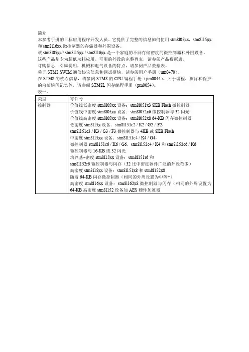
本参考手册的目标应用程序开发人员。
它提供了完整的信息如何使用stm8l05xx,stm8l15xx 和stm8l16xx微控制器的存储器和外围设备。
该stm8l05xx/stm8l15xx/stm8l16xx是一个家庭的不同存储密度的微控制器和外围设备。
这些产品是专为超低功耗应用。
可用的外设的完整列表,请参阅产品数据表。
订购信息,引脚说明,机械和电气设备的特点,请参阅产品数据表。
关于STM8SWIM通信协议信息和调试模块,请参阅用户手册(um0470)。
在STM8的核心信息,请参阅STM8的CPU编程手册(pm0044)。
关于编程,擦除和保护的内部快闪记忆体,请参阅STM8L闪存编程手册(pm0054)。
表一、类型零件号控制器价值线低密度stm8l05xx设备:stm8l051x38KB Flash微控制器价值线中密度stm8l05xx设备:stm8l052x6微控制器与32闪光价值线高密度stm8l05xx设备:stm8l052x864-KB闪存微控制器低密度stm8l15x设备:stm8l151c2/K2/G2/F2,stm8l151c3/K3/G3/F3微控制器与4KB或8KB Flash中密度stm8l15xx设备:stm8l151c4/K4/G4,微控制器stm8l151c6/K6/G6,stm8l152c4/K4和stm8l152c6/K6微控制器与16-KB或32闪光培养基+密度stm8l15xx设备:stm8l151r6和stm8l152r6微控制器与闪存(32比中密度器件广泛的外设范围)高密度stm8l15xx设备:stm8l151x8和stm8l152x8随着64-KB闪存微控制器(相同的外周设置为中等+)高密度stm8l16xx设备:stm8l162x8微控制器与闪存(相同的外周设置为64-KB高密度stm8l152设备加AES硬件加速器1中央处理单元(CPU)。
30。
1.1引言301.2CPU的寄存器。
RM0016Reference manualSTM8S microcontroller familyIntroduction:This reference manual provides complete information for application developers on how to use the STM8S microcontroller memory and peripherals.The STM8S is a family of microcontrollers with different memory sizes, packages and peripherals.■The STM8S is designed for general purpose applications. For ordering information, pin description, mechanical and electrical device characteristics, please refer to the STM8S performance line and access line datasheets.■For information on programming, erasing and protection of the internal Flash memory please refer to the STM8S Flash programming manual (PM0051) and the STM8 SWIM communication protocol and debug module user manual (UM0470)■For information on the STM8 core, please refer to the STM8 CPU programming manual (PM0051)1 Central processing unit (CPU)1.1IntroductionThe CPU has an 8-bit architecture. Six internal registers allow efficient data manipulations.The CPU is able to execute 80 basic instructions. It features 20 addressing modes and can address six internal registers. For the complete description of the instruction set, refer to the STM8 microcontroller family programming manual (PM0044).1.2 CPU registersThe six CPU registers are shown in the programming model in Figure 1. Following an interrupt, the registers are pushed onto the stack in the order shown in Figure 2. They are popped from stack in the reverse order. The interrupt routine must therefore handle it, if needed, through the POP and PUSH instructions.1.2.1 Description of CPU registersAccumulator (A)The accumulator is an 8-bit general purpose register used to hold operands and the results of the arithmetic and logic calculations as well as data manipulations.Index registers (X and Y)These are 16-bit registers used to create effective addresses. They may also be used as a temporary storage area for data manipulations and have an inherent use for some instructions (multiplication/division). In most cases, the cross assembler generates a PRECODE instruction (PRE) to indicate that the following instruction refers to the Y register.Program counter (PC)The program counter is a 24-bit register used to store the address of the next instruction to be executed by the CPU. It is automatically refreshed after each processed instruction. As a result, the STM8 core can access up to 16 Mbytes of memory.Figure 1. Programming modelStack pointer (SP)The stack pointer is a 16-bit register. It contains the address of the next free location of the stack. Depending on the product, the most significant bits can be forced to a preset value.The stack is used to save the CPU context on subroutine calls or interrupts. The user can also directly use it through the POP and PUSH instructions.The stack pointer can be initialized by the startup function provided with the C compiler. For applications written in C language, the initialization is then performed according to the address specified in the linker file for C users. If you use your own linker file or startup file, make sure the stack pointer is initialized properly (with theaddress given in the datasheets).For applications written in assembler, you can use either the startup function provided by ST or write your own by initializing the stack pointer with the correct address.The stack pointer is decremented after data has been pushed onto the stack and incremented after data is popped from the stack. It is up to the application to ensure that the lower limit is not exceeded.A subroutine call occupies two or three locations. An interrupt occupies nine locations to store all the internal registers (except SP). For more details refer to Figure 2. Note: The WFI/HALT instructions save the context in advance. If an interrupt occurs while the CPUis in one of these modes, the latency is reduced.Figure 2. Stacking orderCondition code register (CC)The condition code register is an 8-bit register which indicates the result of the instruction just executed as well as the state of the processor. The 7th bit (MSB) of this register is reserved. These bits can be individually tested by a program and specified action taken as a result of their state. The following paragraphs describeeach bit:●V: OverflowWhen set, V indicates that an overflow occurred during the last signed arithmetic operation, on the MSB result bit. See the INC, INCW, DEC, DECW, NEG, NEGW, ADD, ADDW, ADC, SUB, SUBW, SBC, CP, and CPW instructions.●I1: Interrupt mask level 1The I1 flag works in conjunction with the I0 flag to define the current interruptability level as shown in Table 1. These flags can be set and cleared by software through the RIM, SIM, HALT, WFI, IRET, TRAP, and POP instructions and are automatically set by hardware when entering an interrupt service routine.Table 1. Interrupt levels●H: Half carry bitThe H bit is set to 1 when a carry occurs between the bits 3 and 4 of the ALU during an ADD or ADC instruction. The H bit is useful in BCD arithmetic subroutines.●I0: Interrupt mask level 0See Flag I1.●N: NegativeWhen set to 1, this bit indicates that the result of the last arithmetic, logical or data manipulation is negative (i.e. the most significant bit is a logic 1).●Z: ZeroWhen set to 1, this bit indicates that the result of the last arithmetic, logical or data manipulation is zero.●C: CarryWhen set, C indicates that a carry or borrow out of the ALU occurred during the last arithmetic operation on the MSB operation result bit. This bit is also affected during bit test, branch, shift, rotate and load instructions. See the ADD, ADC, SUB, and SBC instructions.In a division operation, C indicates if trouble occurred during execution (quotient overflow or zero division). See the DIV instruction.In bit test operations, C is the copy of the tested bit. See the BTJF and BTJT instructions. In shift and rotate operations, the carry is updated. See the RRC, RLC, SRL, SLL, and SRA instructions.This bit can be set, reset or complemented by software using the SCF, RCF, and CCF instructions.Example: Addition$B5 + $94 = "C" + $49 = $1491.2.2 STM8 CPU register mapThe CPU registers are mapped in the STM8 address space as shown inTable 2. These registers can only be accessed by the debug module but not by memory access instructions executed in the core.Table 2. CPU register map1.3 Global configuration register (CFG_GCR)1.3.1 Activation levelThe MCU activation level is configured by programming the AL bit in the CFG_GCR register. For information on the use of this bit refer to Section 10.4: Activation level/low power mode control on page 90.1.3.2 SWIM disableBy default, after an MCU reset, the SWIM pin is configured to allow communication with an external tool for debugging or Flash/EEPROM programming. This pin can be configured by the application for use as a general purpose I/O. This is done by setting the SWD bit in the CFG_GCR register.1.3.3 Description of global configuration register (CFG_GCR)Address offset: 0x00Reset value: 0x00Bits 7:2 Reserved, must be kept cleared.Bit 1 AL: Activation levelThis bit is set and cleared by software. It configures main or interrupt-only activation. 0: Main activation level. An IRET instruction causes the context to be retrieved from the stack and the main program continues after the WFI instruction.1: Interrupt-only activation level. An IRET instruction causes the CPU to go back to WFI/halt mode without restoring the context.Bit 0 SWD: SWIM disable0: SWIM mode enabled1: SWIM mode disabledWhen SWIM mode is enabled, the SWIM pin cannot be used as general purpose I/O.1.3.4 Global configuration register map and reset valuesThe CFG_GCR is mapped in the STM8 address space. Refer to the corresponding datasheets for the base address.Table 3. CFG_GCR register map2 Boot ROMThe internal 2 Kbyte boot ROM (available in some devices) contains the bootloader code. Its main task is to download the application program to the internal Flash/EEPROM through the SPI, CAN or UART interface and program the code, data, option bytes and interrupt vectors in the internal Flash/EEPROM.The boot loader starts executing after reset. Refer to the STM8 bootloader user manual (UM0560) for more details.3 Memory and register mapFor details on the memory map, I/O port hardware register map and CPU/SWIM/debug module/interrupt controller registers, refer to the product datasheets.3.1 Register description abbreviationsIn the register descriptions of each chapter in this reference manual, the following abbreviations are used:read/write (rw) :Software can read and write to these bits.read-only (r) :Software can only read these bits.write only (w):Software can only write to this bit. Reading the bit returns a meaningless value.read/write once (rwo):Software can only write once to this bit but, can read it at any time. Only a reset can return this bit to its reset value.read/clear (rc_w1) :Software can read and clear this bit by writing 1. Writing ‘0’ has no effect on the bit value.read/clear (rc_w0):Software can read and clear this bit by writing 0. Writing ‘1’ has no effect on the bit value.read/set (rs): Software can read and set this bit. Writing ‘0’ has no effect on the bit value.read/clear by read (rc_r):Software can read this bit. Reading this bit automatically clears it to ‘0’.Writing ‘0’ has no effect on the bit value.4 Flash program memory and data EEPROM (Flash)4.1 IntroductionThe embedded Flash program memory and data EEPROM memories are controlled by a common set of registers. Using these registers, the application can program or erase memory contents and set write protection, or configure specific low power modes. The application can also program the device option bytes.4.2 Glossary●BlockA block is a set of bytes that can be programmed or erased in one single programming operation. Operations that are performed at block level are faster than standard programming and erasing. Refer to Table 4 for the details on block size.●PageA page is a set of blocks.A dedicated option byte can be used to configure, by increments of one page, the size of the user boot code.4.3 Flash main features●STM8S EEPROM is divided into two memory areas:–Up to 128 Kbytes of Flash program memory. The density differs according to the device. Refer to Section 4.4: Memory organization for details.–Up to 2 Kbytes of data EEPROM including option bytes. Data EEPROM density differs according to the device. Refer to Section 4.4: Memory organization for details.●Programming modes–Byte programming and automatic fast byte programming (without erase operation)–Word programming–Block programming and fast block programming mode (without erase operation) –Interrupt generation on end of program/erase operation and on illegal program operation.●Read-while-write capability (RWW). This feature is not available on all STM8 devices.Refer to the datasheets for details.●In-application programming (IAP) and in-circuit programming (ICP) capabilities ●Protection features–Memory readout protection (ROP)–Program memory write protection with memory access security system (MASS keys).–Data memory write protection with memory access security system (MASS keys) –Programmable write protected user boot code area (UBC)●Memory state configurable to operating or power-down (IDDQ) in halt and Active-halt modes.4.4 Memory organizationSTM8S EEPROM is organized in 32-bit words (4 bytes per word).The memory organization differs according to the devices:●Low density STM8S devices–8 Kbytes of Flash program memory organized in 128 pages of 64 bytes each–640 bytes of data EEPROM organized in 10 pages of 64 bytes each. The data EEPROM includes one block of option bytes (64 bytes)●Medium density STM8S devices–From 16 to 32 Kbytes of Flash program memory organized in up to 64 pages of 512 bytes each.–1 Kbyte of data EEPROM organized in 2 pages of 512 bytes each. The data EEPROM includes one block of option bytes (128 bytes)●High density STM8S devices–From 32 to 128 Kbytes of Flash program memory organized in up to 256 pages of 512 bytes each–From 1 to 2 Kbytes of data EEPROM organized in up to 4 pages of 512 bytes each. The data EEPROM includes one block of option bytes (128 bytes)The page defines the granularity of the user boot code area as described in Section4.4.2:User boot area (UBC).Figure 3, Figure 4, and Figure 5 show the Flash memory and data EEPROM organization for STM8S devices.Note: The EEPROM access time allows the device to run up to 16 MHz. For clock frequencies above 16 MHz, Flash/data EEPROM access must be configured for 1 wait state. This is enabled by the device option byte (refer to the option bytes section of the STM8S datasheets).4.4.1 Memory access/ wait state configurationThe Flash/ data EEPROM access time allows the device to run at up to 16 MHz without waitstates.When using the high-speed external clock (HSE) at higher frequencies up to 24 MHz, one wait state is necessary. In this case the device option byte should be programmed to insert this wait state. Refer to the datasheet option byte section.Figure 3. Flash memory and data EEPROM organization on low density STM8S Figure 4. Flash memory and data EEPROM organization on medium density STM8SFigure 5. Flash memory and data EEPROM organization high density STM8S4.4.2 User boot area (UBC)The user boot area (UBC) contains the reset and the interrupt vectors. It can be used to store the IAP and communication routines. The UBC area has a second level of protection to prevent unintentional erasing or modification during IAP programming. This means that it is always write protected and the write protection cannot be unlocked using the MASS keys.The size of the UBC area can be obtained by reading the UBC option byte.The size of the UBC area can be configured in ICP mode (using the SWIM interface) through the UBC option byte. The UBC option byte specifies the number of pages allocated for the UBC area starting from address 0x00 8000.Refer to Figure 6, Figure 7 and Figure 8 for a description of the UBC area memory mapping and to the option byte section in the datasheets for more details on the UBC option byte.Figure 6. UBC area size definition on low density STM8S devices1. N (number of protected pages) = UBC[7:0].2. UBC[7:0] = 0x00 means no user boot code area is defined. Refer to the datasheets for the description of the UBC option byte.3. The first 2 pages (128 bytes) contain the interrupt vectors.Figure 7. UBC area size definition on medium density STM8S1. N (number of protected pages) = UBC[7:0] + 2 for UBC[7:0] > 1.2. UBC[7:0] =0x00 means no user boot code area is defined. Refer to the datasheets for the description of the UBC option byte.3. The first 2 pages (1 Kbytes) contain the 128 bytes of interrupt vectors (32 IT vectors).Figure 8. UBC area size definition on high density STM8S1. UBC[7:0] = 0x00 means no user boot code area is defined. Refer to the datasheets for the description of the UBC option byte.2. The first 2 pages (1 Kbytes) contain the interrupt vectors, of which only 128 bytes (32 IT vectors) are used.4.4.3 Data EEPROM (DATA)The data EEPROM area can be used to store application data. By default, the DATA area is write protected to prevent unintentional modification when the main program is updated in IAP mode. The write protection can be unlocked only by using a specific MASS key sequence (refer to Enabling write access to the DATA area).Refer to Section 4.4: Memory organization for the size of the DATA area according to the STM8S devices.4.4.4 Main program areaThe main program is the part of the Flash program memory which is used to store theapplication code (see Figure 3, Figure 4 and Figure 5).4.4.5 Option bytesThe option bytes are used to configure device hardware features and memory protection.They are located in a dedicated memory array of one block.The option bytes can be modified both in ICP/SWIM and in IAP mode, with OPT bit of the FLASH_CR2 register set to 1 and the NOPT bit of the FLASH_NCR2 register set to 0 (see Section 4.8.2: Flash control register 2 (FLASH_CR2) and Section 4.8.3: Flash complementary control register 2 (FLASH_NCR2)).Refer to the option byte section in the datasheet for more information on option bytes, and to the STM8 SWIM protocol and debug module user manual (UM0470) for details on how to program them.4.5 Memory protection4.5.1 Readout protectionReadout protection is selected by programming the ROP option byte to 0xAA. When readout protection is enabled, reading or modifying the Flash program memory and DATA area in ICP mode (using the SWIM interface) is forbidden, whatever the write protection settings. Even if no protection can be considered as totally unbreakable, the readout feature provides a very high level of protection for a general purpose microcontroller.The readout protection can be disabled on the program memory, UBC, and DATA areas, by reprogramming the ROP option byte in ICP mode. In this case, the Flash program memory, the DATA area and the option bytes are automatically erased and the device can be reprogrammed.Refer to Table 5: Memory access versus programming method for details on memory access when readout protection is enabled or disabled.4.5.2 Memory access security system (MASS)After reset, the main program and DATA areas are protected against unintentional write operations. They must be unlocked before attempting to modify their content. This unlock mechanism is managed by the memory access security system (MASS). The UBC area specified in the UBC option byte is always write protected (see Section 4.4.2:User boot area (UBC)).Once the memory has been modified, it is recommended to enable the write protection again to protect the memory content against corruption.Enabling write access to the main program memoryAfter a device reset, it is possible to disable the main program memory write protection by writing consecutively two values called MASS keys to theFLASH_PUKR register (see Section 4.8.6: Flash program memory unprotecting key register (FLASH_PUKR)). These programmed keys are then compared to two hardware key values:●First hardware key: 0b0101 0110 (0x56)●Second hardware key: 0b1010 1110 (0xAE)The following steps are required to disable write protection of the main program area: 1. Write a first 8-bit key into the FLASH_PUKR register. When this register is written for the first time after a reset, the data bus content is not latched into the register, but compared to the first hardware key value (0x56).2. If the key available on the data bus is incorrect, the FLASH_PUKR register remains locked until the next reset. Any new write commands sent to this address are discarded.3. If the first hardware key is correct when the FLASH_PUKR register is written for the second time, the data bus content is still not latched into the register, but compared to the second hardware key value (0xAE).4. If the key available on the data bus is incorrect, the write protection on program memory remains locked until the next reset. Any new write commands sent to this address is discarded.5. If the second hardware key is correct, the main program memory is write unprotected and the PUL bit of the FLASH_IAPSR is set (see Section 4.8.8: Flash status register (FLASH_IAPSR) register.Before starting programming, the application must verify that PUL bit is effectively set. The application can choose, at any time, to disable again write access to the Flash program memory by clearing the PUL bit.Enabling write access to the DATA area After a device reset, it is possible to disable the DATA area write protection by writing consecutively two values called MASS keys to the FLASH_DUKR register (see Section 4.8.9: Flash register map and reset values). These programmed keys are then compared to two hardware key values:●First hardware key: 0b1010 1110 (0xAE)●Second hardware key: 0b0101 0110 (0x56)The following steps are required to disable write protection of the DATA area:1. Write a first 8-bit key into the FLASH_DUKR register. When this register is written for the first time after a reset, the data bus content is not latched into the register, but compared to the first hardware key value (0xAE).2. If the key available on the data bus is incorrect, the application can re-enter two MASS keys to try unprotecting the DATA area.3. If the first hardware key is correct, the FLASH_DUKR register is programmed with the second key. The data bus content is still not latched into the register, but compared to the second hardware key value (0x56).4. If the key available on the data bus is incorrect, the data EEPROM area remains write protected until the next reset. Any new write command sent to this address isignored.5. If the second hardware key is correct, the DATA area is write unprotected and the DUL bit of the FLASH_IAPSR register is set (see Section 4.8.8: Flash status register (FLASH_IAPSR)).Before starting programming, the application must verify that the DATA area is not write protected by checking that the DUL bit is effectively set. The application can choose, at any time, to disable again write access to the DATA area by clearing the DUL bit.4.5.3 Enabling write access to option bytesThe procedure for enabling write access to the option byte area is the same as the one used for data EEPROM. However, the OPT bit in the Flash control register 2 (FLASH_CR2) must be set, and the corresponding NOPT bit in the Flash complementary control register 2 (FLASH_NCR2) must be cleared to enable write access to the option bytes.。
stm:Bootloader1.项目介绍在之前的例程和实践中,我们都是使用st-link调试下载的方式进行程序烧录。
大家可能已经认识到这种烧录方式的弊端了。
因为这种烧录方式首先必须要有以下几个工具或者软件:1.烧录工具(不能芯片支持的工具不一样,有ST-Link,JTAG等)2.已经安装了IDE(IAR或者SVD或者CCS等)或者与烧录工具匹配的烧录软件的电脑3.烧录前后需要物理上电掉电(不建议ST-Link进行热插拔),即开/关电源.也许大家会觉得,对于学习而言,这些都能忍受。
但是如果真正做成产品,如果还是用这种方式进行升级,那代价就太大。
举个例子吧,我之前的工作是开发和维护大功率的UPS(不间断电源),主要客户是一些大型企业,例如银行的数据中心,中国移动网络中心。
UPS内部有许多ARM芯片,DSP芯片。
这类应用场合,即便给程序升级,客户也不会让你断电的,而且因为安全性要求,一般MCU,DSP都是在产品内部,根本无法对外开放烧录盒的烧录接口。
所以绝大部分嵌入式产品,都会开发Bootloader程序。
那么什么是Boot Loader呢?一般来说,嵌入式产品的软件都会分为两部分,第一部分为Bootloader,第二部分为主程序(Main APP),它们存放在flash的不同区域。
Bootloader是上电或者复位以后先执行的,通过它,我们可以初始化硬件设备、建立内存空间的映射图,检测程序的完整性,判断是否需要从Bootloader 跳转到APP或者更新APP。
而主程序呢,则是真正用来实现产品面向客户的功能的。
通常呢,在Bootloader会实现一种或者一种以上的IAP方式,可能是UART,SPI,CAN或者Ethernet等。
本次例程呢,就是设计一个Bootloader,允许用户用电脑的串口+超级终端实现烧录功能2.程序流程设计秉承软件开发好习惯,coding前先想好思路,设计好流程框图,coding时才能事半功倍哦。
June 2011Doc ID 14614 Rev 31/27PM0051Programming manualHow to program STM8S and STM8A Flash program memory and data EEPROMIntroductionThis manual describes how to program Flash program memory and data EEPROM onSTM8 microcontrollers. It applies to access and performance line STM8S and medium and high density STM8A devices. It is intended to provide information to the programming tool manufacturers and to the customers who want to implement programming by themselves on their production line.The in-circuit programming (ICP) method is used to update the content of Flash program memory and data EEPROM while the user software is not running. It uses the Single wire interface module (SWIM) to communicate between the programming tool and the device.In contrast to the ICP method, in-application programming (IAP) can use anycommunication interface supported by the microcontroller (I/Os, SPI, USART , I 2C, USB, CAN...). IAP has been implemented for users who want their application software to update itself by re-programming the Flash program memory during program execution. The main advantage of IAP is its ability to re-program Flash program memory and data EEPROM when the chip has already been soldered on the application board and while the usersoftware is running. Nevertheless, part of the Flash program memory has to be previously programmed using ICP .Some devices also contain a bootloader embedded in a ROM memory. Through this firmware the device memory can be re-programmed using a standard communication interface. This programming method is not described in this document.For details on memory implementation and features, registers or stack top addresses, refer to the product datasheets.Related documents●STM8 SWIM communication protocol and debug module (UM0470)●STM8 bootloader user manual (UM0560)l●STM8S and STM8A microcontroller families reference manual (RM0016)●Basic in-application programming example using the STM8 I 2C and SPI peripherals (AN2737)●STM8 in-application programming example (AN2659)●Performance line datasheet (high density Flash program and data EEPROM)●Access line datasheets (low and medium density Flash program and data EEPROM)●STM8A datasheets (up to 32 Kbytes and up to 128Kbytes of Flash program memory)Contents PM0051Contents1Glossary . . . . . . . . . . . . . . . . . . . . . . . . . . . . . . . . . . . . . . . . . . . . . . . . . . . 42Memory organization . . . . . . . . . . . . . . . . . . . . . . . . . . . . . . . . . . . . . . . . 62.1Low density STM8S microcontrollers . . . . . . . . . . . . . . . . . . . . . . . . . . . . . 62.2Medium density STM8S microcontrollers . . . . . . . . . . . . . . . . . . . . . . . . . . 72.3High density STM8S microcontrollers . . . . . . . . . . . . . . . . . . . . . . . . . . . . 92.4Medium density STM8A microcontrollers . . . . . . . . . . . . . . . . . . . . . . . . . 102.5High density STM8A microcontrollers . . . . . . . . . . . . . . . . . . . . . . . . . . . 123Memory protection strategy . . . . . . . . . . . . . . . . . . . . . . . . . . . . . . . . . . 143.1Readout protection . . . . . . . . . . . . . . . . . . . . . . . . . . . . . . . . . . . . . . . . . . 143.2User Boot Code area protection . . . . . . . . . . . . . . . . . . . . . . . . . . . . . . . . 153.3Unwanted memory access protection . . . . . . . . . . . . . . . . . . . . . . . . . . . 154Programming STM8 Flash microcontrollers . . . . . . . . . . . . . . . . . . . . . 164.1Unlocking the Memory Access Security System (MASS) . . . . . . . . . . . . 164.2Block programming . . . . . . . . . . . . . . . . . . . . . . . . . . . . . . . . . . . . . . . . . 164.3Word programming . . . . . . . . . . . . . . . . . . . . . . . . . . . . . . . . . . . . . . . . . . 204.4Byte programming . . . . . . . . . . . . . . . . . . . . . . . . . . . . . . . . . . . . . . . . . . 214.5Programming the option bytes . . . . . . . . . . . . . . . . . . . . . . . . . . . . . . . . . 224.5.1Summary of memory dedicated option bytes . . . . . . . . . . . . . . . . . . . . 224.5.2How to program the option bytes . . . . . . . . . . . . . . . . . . . . . . . . . . . . . . 224.6Memory access versus programming method . . . . . . . . . . . . . . . . . . . . . 234.6.1ICP methods . . . . . . . . . . . . . . . . . . . . . . . . . . . . . . . . . . . . . . . . . . . . . 244.6.2IAP method . . . . . . . . . . . . . . . . . . . . . . . . . . . . . . . . . . . . . . . . . . . . . . 25 5Flash program memory and data EEPROM comparison . . . . . . . . . . . 25 6Revision history . . . . . . . . . . . . . . . . . . . . . . . . . . . . . . . . . . . . . . . . . . . 262/27Doc ID 14614 Rev 3PM0051List of tables List of tablesTable 1.Low density STM8S memory partition . . . . . . . . . . . . . . . . . . . . . . . . . . . . . . . . . . . . . . . . . 7 Table 2.Medium density STM8S memory partition . . . . . . . . . . . . . . . . . . . . . . . . . . . . . . . . . . . . . . 8 Table 3.High density STM8S memory partition. . . . . . . . . . . . . . . . . . . . . . . . . . . . . . . . . . . . . . . . . 9 Table 4.Medium density STM8A memory partition . . . . . . . . . . . . . . . . . . . . . . . . . . . . . . . . . . . . . 11 Table 5.High density STM8A memory partition. . . . . . . . . . . . . . . . . . . . . . . . . . . . . . . . . . . . . . . . 12 Table 6.Recommended minimum and maximum sizes of the UBC area . . . . . . . . . . . . . . . . . . . . 15 Table 7.MASS . . . . . . . . . . . . . . . . . . . . . . . . . . . . . . . . . . . . . . . . . . . . . . . . . . . . . . . . . . . . . . . . . 16 Table 8.Memory access versus programming method . . . . . . . . . . . . . . . . . . . . . . . . . . . . . . . . . . 23 Table parison between STM8S and STM8A devices . . . . . . . . . . . . . . . . . . . . . . . . . . . . . . 25 Table 10.Document revision history . . . . . . . . . . . . . . . . . . . . . . . . . . . . . . . . . . . . . . . . . . . . . . . . . 26Doc ID 14614 Rev 33/27Glossary PM0051 1 GlossaryThis section gives a brief definition of acronyms and terms used in this document:●BlockA block is a set of bytes that can be programmed or erased in one single programmingoperation. Operations that are available on a block are fast programming, erase only,and standard programming (which includes an erase operation). Refer to Section2:Memory organization for details on block size according to the device.●BootloaderThe bootloader is an IAP application embedded in the system memory of the device. Itis used to erase and program the device using a standard serial communication port.The bootloader is not available on small devices, and is not described in the presentdocument. Refer to STM8 bootloader user manual (UM0500) for more details.●DriverA driver is a control program defined by the application developer. It is used to managethe allocation of system resources to start application programs. In this document twodrivers are described, ICP and IAP drivers.●In-application programming (IAP)IAP is the ability to re-program the Flash program memory and data EEPROM (DAT A)of a microcontroller while the device is already plugged-in to the application and theapplication is running.●In-circuit programming (ICP)ICP is the ability to program the Flash program memory and data EEPROM of amicrocontroller using the SWIM protocol while the device is plugged-in to theapplication.●In-circuit debugging (ICD)ICD is the ability to debug the user software using the SWIM protocol. The user has theability to connect the device to a debugger and insert breakpoints in his firmware.Debugging may be intrusive (application patched to allow debugging) or non intrusive(using a debug module).●Memory access security system (MASS) keysThe Memory access security system (MASS) consists of a memory write protectionlock designed to prevent unwanted memory modifications due to EMS or programcounter loss. To unlock the memory protection, one or more keys must be written in adedicated register and in a specific order. When the operation (write or erase) iscompleted, the MASS must be activated again to provide good memory security.4/27 Doc ID 14614 Rev 3PM0051Glossary●PageA page is a set of blocks. The number of blocks in a page may differ from one device toanother. Refer to Section2: Memory organization for details on page size according tothe device.A dedicated option byte can be used to configure by increments of one page the size ofthe user boot code. Refer to Section5: Flash program memory and data EEPROMcomparison for a description of available areas and option bytes according to thedevices.●Read-while-write (RWW)The RWW feature provides the ability for the software to perform write operation ondata EEPROM while reading and executing the program memory. Execution time istherefore optimized. The opposite operation is not allowed: the software cannot readdata memory while writing program memory.The RWW feature is not available on all STM8 devices. Refer to Table9 for informationon devices with RWW capability.●Single wire interface module (SWIM)The SWIM is a communication protocol managed by hardware in the STM8microcontrollers. The SWIM main purpose is to provide non intrusive debug capability.It can also be used to download programs into RAM and execute them. It can also write(registers or RAM) or read any part of the memory space and jump to any memoryaddress. The SWIM protocol is used for ICP. It is accessed by providing a specificsequence on the SWIM pin either during the reset phase or when the device is running(if allowed by the application).●System memoryThe STM8 system memory is a small ROM accessible when the user software isexecuted. It contains the bootloader. The system ROM and the bootloader are notavailable on all STM8 devices.●User boot code area (UBC)The user boot code area is a write-protected area which contains reset vector, interruptvectors, and IAP routine for the device to be able to recover from interrupted orerroneous IAP programming.●User modeThe user mode is the standard user software running mode in the STM8. It is enteredeither by performing a power-on-reset on the device or by issuing the SWIM SRSTcommand from a development tool.●WordA word is a set of 4 bytes and corresponds to the memory granularity.Doc ID 14614 Rev 35/27Memory organization PM00516/27 Doc ID 14614 Rev 32 Memory organizationThis section describes the memory organization corresponding to:●Access line and performance line STM8S microcontrollers ●Medium and high density STM8A microcontrollersSTM8S microcontrollers offer low density (8Kbytes), medium density (from 16 to32Kbytes) and high density (from 32 to 128Kbytes) Flash program memory, plus data EEPROM.STM8A microcontrollers feature medium density (from 8 to 32Kbytes) and high density (from 32 to 128Kbytes) Flash memory, plus data EEPROM.The memory organization differs from one STM8 family to another. Refer to Section 2.1, Section 2.2, Section 2.3, Section 2.4, and Section 2.3 for a description of the memory organization according to microcontroller family and memory density.A memory accelerator takes advantage of the parallel 4-byte storage, which corresponds to a word. The Flash program memory and data EEPROM can be erased and programmed at byte level, word level or block level. In word programming mode, 4 bytes can beprogrammed/erased during the same cycle, while in block programming mode, a whole block is programmed/erase during the same cycle. Refer to Section 2.1, Section 2.2, Section 2.3, Section 2.4, and Section 2.3 for information on block size according to the devices.2.1 Low density STM8S microcontrollersThe memory array is divided into two areas:●8Kbytes of Flash program memory organized in 128 pages or blocks of 64 bytes each. The Flash program memory is divided into 2 areas, the user boot code area (UBC), which size can be configured by option byte, and the main program memory area. The Flash program memory is mapped in the upper part of the STM8S addressing space and includes the reset and interrupt vectors.●640 bytes of data EEPROM (DATA) organized in 10 pages or blocks of 64bytes each. One block (64bytes) contains the option bytes of which 11 are used to configure the device hardware features. The options bytes can be programmed in user, IAP and ICP/SWIM modes.Refer to T able 1 for a detailed description of the memory partition for low density STM8S microcontrollers.PM0051Memory organizationDoc ID 14614 Rev 37/272.2 Medium density STM8S microcontrollersThe memory is divided into two arrays:●From 16 to 32Kbytes of Flash program memory organized in up to 64 pages of 4blocks of 128 bytes each. The Flash program memory is divided into 2 areas, the user boot code area (UBC), which size can be configured by option byte, and the mainprogram memory area. The Flash program memory is mapped in the upper part of the STM8S addressing space and includes the reset and interrupt vectors.●1Kbytes of data EEPROM (DATA) organized in up to 2 pages of 4 blocks of 128bytes each. One block (128 bytes) contains the option bytes of which 13 are used toconfigure the device hardware features. The options bytes can be programmed in user, IAP and ICP/SWIM modes.Refer to T able 2 for a detailed description of the memory partition for medium density STM8S microcontrollers.Table 1.Low density STM8S memory partitionAreaPage number (1 page=1 block)Block number (1 block=64bytes)Address Data EEPROM000x004000-0x00403F 110x004040-0x00407F 220x004080-0x0040BF (9)90x004240-0x00427F Option bytes -0 (one block only)0x004800-0x00483F Flash program memory000x008000-0x00803F 110x008040-0x00807F 220x008080-0x0080BF (127)1270x009FC0-0x009FFFMemory organization PM00518/27 Doc ID 14614 Rev 3Table 2.Medium density STM8S memory partition (1)AreaPage number (1 page=4 blocks)Block number (1 block=128bytes)Address Data EEPROM 000x004000-0x00407F 10x004080-0x0040FF 20x004100-0x00417F 30x004180-0x0041FF 14-70x004200-0x0043FF Option bytes -0 (one block only)0x004800-0x00487F Flash program memory00x008000-0x00807F 10x008080-0x0080FF 20x008100-0x00817F 30x008180-0x0081FF 14-70x008200-0x0083FF... (63)2520x00FE00-0x00FE7F 2530x00FE80-0x00FEFF 2540x00FF00-0x00FF7F 2550x00FF80-0x00FFFF1.The memory mapping is given for the devices featuring 32Kbytes of Flash program memory.PM0051Memory organizationDoc ID 14614 Rev 39/272.3 High density STM8S microcontrollersThe memory is divided into two arrays:●From 32 to 128Kbytes of Flash program memory organized in up to 256 pages of 4 blocks of 128 bytes each. The Flash program memory is divided into 2 areas, the user boot code area (UBC), which size can be configured by option byte, and the mainprogram memory area. The Flash program memory is mapped in the upper part of the STM8S addressing space and includes the reset and interrupt vectors.●From 1 to 2Kbytes of data EEPROM (DATA) organized in up to 4 pages of 4 blocks of 128bytes each. The size of the DATA area is fixed for a given microcontroller. One block (128bytes) contains the option bytes of which 15 are used to configure the device hardware features. The options bytes can be programmed in user, IAP and ICP/SWIM modes.Refer to T able 3 for a detailed description of the memory partition for high density STM8S microcontrollers.Table 3.High density STM8S memory partition (1)AreaPage number (1 page=4 blocks)Block number (1 block=128bytes)Address Data EEPROM00x004000-0x00407F 10x004080-0x0040FF 20x004100-0x00417F 30x004180-0x0041FF 1 4 to 70x004200-0x0043FF 28 to 110x004400-0x0045FF 312 to 150x004600-0x0047FF Option bytes-0 (one block only)0x004800-0x00487FMemory organization PM005110/27 Doc ID 14614 Rev 32.4 Medium density STM8A microcontrollersThe memory is divided into two arrays:●From 8 to 32Kbytes of Flash program memory organized in up to 64 pages of 4 blocks of 128 bytes each. The Flash program memory is divided into 2 areas, the user boot code area (UBC), which size can be configured by option byte, and the main program memory area. The Flash program memory is mapped in the upper part of the STM8A addressing space and includes the reset and interrupt vectors.●From 384 bytes to 1Kbytes of data EEPROM (DATA) organized in up to 2 pages of 4 blocks of 128bytes each. One block (128 bytes) contains the option bytes of which 13 are used to configure the device hardware features. The options bytes can be programmed in user, IAP and ICP/SWIM modes.Refer to T able 4 for a detailed description of the memory partition for medium density STM8A microcontrollers.Flash program memory00x008000-0x00807F 10x008080-0x0080FF 20x008100-0x00817F 30x008180-0x0081FF 14 to 70x00 8200-0x00 83FF 28 to 110x00 8400-0x00 85FF... (255)10200x00 27E00-0x00 27E7F 10210x00 27E80-0x00 27EFF 10220x00 27F00-0x00 27F7F 10230x00 27F80-0x00 27FFF1.The memory mapping is given for the devices featuring 128Kbytes of Flash program memory and 2Kbytes of dataEEPROM.Table 3.High density STM8S memory partition (1) (continued)AreaPage number (1 page=4 blocks)Block number (1 block=128bytes)AddressPM0051Memory organizationDoc ID 14614 Rev 311/27Table 4.Medium density STM8A memory partition (1)AreaPage number (1 page=4 blocks)Block number (1 block=128bytes)Address Data EEPROM 000x004000-0x00407F 10x004080-0x0040FF 20x004100-0x00417F 30x004180-0x0041FF 14-70x004200-0x0043FF Option bytes -0 (one block only)0x004800-0x00487F Flash program memory00x008000-0x00807F 10x008080-0x0080FF 20x008100-0x00817F 30x008180-0x0081FF 14-70x008200-0x0083FF... (63)2520x00FE00-0x00FE7F 2530x00FE80-0x00FEFF 2540x00FF00-0x00FF7F 2550x00FF80-0x00FFFF1.The memory mapping is given for the devices featuring 32Kbytes of Flash program memory.Memory organization PM005112/27 Doc ID 14614 Rev 32.5 High density STM8A microcontrollersThe memory is divided into two arrays:●From 32 to 128Kbytes of Flash program memory organized in up to 256 pages of 4 blocks of 128 bytes each. The Flash program memory is divided into 2 areas, the user boot code area (UBC), which size can be configured by option byte, and the mainprogram memory area. The Flash program memory is mapped in the upper part of the STM8A addressing space and includes the reset and interrupt vectors.●From 1 to 2Kbytes of data EEPROM (DATA) organized in up to 4 pages of 4 blocks of 128bytes each. The size of the DATA area is fixed for a given microcontroller. One block (128bytes) contains the option bytes of which 15 are used to configure the device hardware features. The options bytes can be programmed in user, IAP and ICP/SWIM modes.Refer to T able 5 for a detailed description of the memory partition for high density STM8A microcontrollers.Table 5.High density STM8A memory partition (1)AreaPage number (1 page=4 blocks)Block number (1 block=128bytes)Address Data EEPROM00x004000-0x00407F 10x004080-0x0040FF 20x004100-0x00417F 30x004180-0x0041FF 1 4 to 70x004200-0x0043FF 28 to 110x004400-0x0045FF 312 to 150x004600-0x0047FF Option bytes-0 (one block only)0x004800-0x00487FPM0051Memory organizationDoc ID 14614 Rev 313/27Flash program memory00x008000-0x00807F 10x008080-0x0080FF 20x008100-0x00817F 30x008180-0x0081FF 14 to 70x00 8200-0x00 83FF 28 to 110x00 8400-0x00 85FF... (255)10200x00 27E00-0x00 27E7F 10210x00 27E80-0x00 27EFF 10220x00 27F00-0x00 27F7F 10230x00 27F80-0x00 27FFF1.The memory mapping is given for the devices featuring 128Kbytes of Flash program memory and 2Kbytes of dataEEPROM.Table 5.High density STM8A memory partition (1) (continued)AreaPage number (1 page=4 blocks)Block number (1 block=128bytes)Address3 Memory protection strategyThe STM8 devices feature several mechanisms allowing to protect the content of the Flashprogram and data EEPROM areas:●Readout protectionThe software can prevent application code and data stored in the Flash programmemory and data EEPROM from being read and modified in ICP/SWIM mode. Thereadout protection is enabled and disabled by programming an option byte inICP/SWIM mode. Refer to Section3.1 for details.●User boot code area (UBC)In order to guaranty the capability to recover from an interrupted or erroneous IAPprogramming, all STM8 devices provide a write-protected area called user boot code(UBC). This area is a part of the Flash program memory which cannot be modified inuser mode (that is protected against modification by the user software). The content ofthe UBC area can be modified only in ICP/SWIM mode after clearing the UBC optionbyte.The size of the user boot code area can be configured through an option byte byincrements of one page.Refer to Section3.2 for details on user boot code area.●Unwanted memory access protectionAll STM8 devices offer unwanted memory access protection, which purpose is toprevent unintentional modification of program memory and data EEPROM (for exampledue to a firmware bug or EMC disturbance).This protection consists of authorizing write access to the memory only through aspecific software sequence which is unlikely to happen randomly or by mistake. Accessto Flash program and data EEPROM areas is enabled by writing MASS keys into keyregisters.Refer to Section3.3 for details on unwanted memory access protection.protection3.1 ReadoutThe readout protection is enabled by writing 0xAA in the ROP option byte. It is disabled byreprogramming the ROP option byte with any value except for 0xAA and resetting thedevice.The readout protection can only be disabled in ICP/SWIM mode.When the readout protection is selected, reading or modifying the Flash program memory inICP mode (using the SWIM interface) is forbidden. When available, the data EEPROMmemory is also protected against read and write access through ICP.Erasing the ROP option byte to disable the readout protection causes the Flash programmemory, the DATA area and the option bytes to be erased.Even though no protection can be considered as totally unbreakable, the readout protectionfeature provides a very high level of protection for general purpose microcontrollers. Ofcourse, a software that allows the user to dump the Flash program memory content makethis readout protection useless. Table8 describes possible accesses to each memory areasversus the different modes and readout protection settings.14/27 Doc ID 14614 Rev 3Doc ID 14614 Rev 315/273.2 User Boot Code area protectionWhatever the memory content, it is always possible to restart an ICP session after a critical error by applying a reset and restarting the SWIM communication.On the contrary, during IAP sessions, the programming software driver must always be write protected to be able to recover from any critical failure that might happen during programming (such as power failure).The pages where the IAP driver is implemented must be located in the write-protected boot code area (UBC). The application reset and interrupt vectors and the reset routine must also be stored in the UBC. These conditions allow the user software to manage the recovery from potential critical failure by applying a reset and restarting the IAP routine from the protected boot area.The UBC size is defined by the user boot code (UBC) area option byte. This option byte may slightly differ from one product to another. See the following table for the minimum and maximum size of the UBC area. Its maximum size is equal to the full memory size3.3 Unwanted memory access protectionThe unwanted memory access protection consists of writing two 8-bit keys in the right order into dedicated MASS key registers.Writing the correct sequence of keys in the program memory MASS key register(FLASH_PUKR) enables the programming of the program memory area excluding the UBC. If wrong keys are provided, a reset must to be generated to be able to reprogram the right keys.Once the write memory protection has been removed, it is possible to reactivate the protection of the area by resetting the PUL bit in FLASH_IAPSR.To enable write access to the data EEPROM area, another specific MASS key register (FLASH_DUKR) and a different key sequence must be used. Once the dataEEPROM/option byte area is unlocked, it is possible to reactivate the protection of the area by resetting the DUL bit in FLASH_IAPSR.If wrong keys have been provided to the FLASH_PUKR register, the device must be reset before performing a new key program sequence. However, when wrong keys are provided to the FLASH_DUKR register, new keys can be entered without the device being previously reset.In order to be as effective as possible, the application software must lock again theunwanted memory access protection as soon as the programming is completed. Otherwise, the protection level of the MASS is significantly reduced. To activate the MASS protection again, the user must reset the corresponding bits in the FLASH_IAPSR register (DUL bit for data EEPROM or PUL bit for Flash program memory).Table 6.Recommended minimum and maximum sizes of the UBC areaSTM8 microcontroller familyRecommended minimum sizeof the UBC areaMaximum size of the UBC areaLow density STM8S2 pages = 128bytes Full memory size Medium density STM8S and STM8A 2 pages = 1KbyteFull memory sizeHigh density STM8S and STM8A16/27 Doc ID 14614 Rev 3Note:1The mechanism to lock and unlock unwanted memory access protection is identical for option bytes and data EEPROM (see Ta ble 7: MASS ).2Before starting programming program memory or data EEPROM, the software must verify that the area is not write protected by checking that the PUL or DUL bit is effectively set.4 Programming STM8 Flash microcontrollersThis section describes how to program STM8 single-voltage Flash microcontrollers.4.1 Unlocking the Memory Access Security System (MASS)The memory must be unlocked before attempting to perform any erase or write operation. To unlock it, follow the procedure described in Section 3.3: Unwanted memory access protection , and Table 7.The software must poll the PUL and DUL bit, before attempting to write to program memory and data EEPROM, respectively.4.2 Block programmingBlock write operations allow to program an entire block in one shot, thus minimizing theprogramming time.There are three possible block programming modes: erase, write only (also called fast programming) and combined erase/write cycle (also called standard block programming).Table 7.MASSMicrocontrollerfamilyData EEPROM and option bytes Program memoryUnlock Lock Unlock Lock STM8S and STM8AWrite 0xAE then56h in FLASH_DUKR (0x00 5064)(1)(2)1.The OPT and NOPT bits of FLASH_CR2 and FLASH_NCR2 registers must be set/cleared to enableaccess to the option bytes.2.If wrong keys have been entered, another key programming sequence can be issued without resetting thedevice.Reset bit 3 (DUL) in FLASH_IAPSR (0x00 505F)Write 0x56 then0xAE in FLASH_PUKR (0x00 5062)(3)3.If wrong keys have been entered, the device must be reset, and a key program sequence issued.Reset bit 1 (PUL) in FLASH_IAPSR (0x00 505F)。
1简介。
顺哥STM8开发板是一款基于STM8系列单片机的开发板,班上固有的外设可以完成CAN总线串口通信,电容触摸按键和电容触摸划块实验,可以完成相应的实验。
本文档只是对板子的简单使用做了简单的说明,并且对板子的几个程序进行了简要的说明2开发板的简介2.1开发板布局(/item.htm?id=133********)2.2板子跟仿真器的链接2.2.1ST LINK III仿真器简介(/item.htm?id=12415784614)ST-LINK III仿真器是ST意法半导体为初学者学习、评估、开发STM32系列ARM MCU设计的仿真开发工具。
ST-LINK II配合IAR Systems EWARM集成开发环境,是STM32系列初学者学习入门、软件编程调试的最佳开发工具。
2.2.2仿真器的特点支持全系列STM32/STM8S系列MCU,USB2.0全速,·下载速度大于20Kb/秒自适应目标系统JTAG电平3.3V-5V标准20芯JTAG仿真插座.与其他的仿真器相比,ST link III,非常方便,无需单独安装设备驱动,即插即用。
不足的是仿真器的速度不高。
2.2.3仿真器与顺哥STM8S208开发板的连接在正常的链接之后拔掉下载选择跳线帽可以进行仿真2.2.4硬件仿真在仿真器跟板子连接之后,我们打开编译软件STVD在程序编译通过之后,设置编译器然后点击“Debug”按键可以观察到仿真器上面的小灯,闪烁,正常的进行仿真。
2.2.5仿真处理当我们第一次用仿真器向STM8S208RB的单片机烧写某些程序的时候会出现下图所示的错误这是由于没有烧写过程序的STM8S208RB单片机里面的USB区域的一部分是写保护的,只要将UBC区域的写保护去除即可,如图正是由于UBC的部分区域被保护,所以STM8S208RB单片机的程序串口下载跟其他的STM8系列单片机有所不同。
2.3串口下载大多数的单片机可以进行串口下载,STM8S系列单片机也不例外,也可以进行串口下载,使用软件flash Loader Demo在STM8S208RB单片机的在没有进行UBC区域解锁的时候,是没有办发进行程序下载的,即使能够进入程序下载界面也没有办法将程序烧如单片机,所以下面进行的操作是在UBC区域解锁之后.,并且使用顺哥的STM8S208开发板时的设置,其他的板子和单片机型号不可。
STM8A车用微控制器的新安全手册资料包可简化ISO 26262认证流程中国,2015年8月17日——意法半导体(STMicroelectronics,简称ST;纽约证券交易所代码:STM)发布新安全手册及FMEDA文档,帮助汽车厂商及供应商简化基于STM8AF 车用微控制器的汽车系统通过ISO 26262功能性安全认证流程。
最高可取得汽车安全完整性等级标准ASIL-B证书。
意法半导体通过AEC-Q100认证的STM8AF是深受市场欢迎的经济型微控制器产品,具有包括CAN和LIN驱动器、触控感测 / LCD控制等多项实用功能,被广泛用于车身控制及车用信息娱乐系统,例如座椅调节、仪表显示和照明控制。
其可靠的运行能力可大幅度提升乘坐舒适度及驾驶员的注意力,以实现更优质、更安全的用户体验,汽车一级供应商致力于设计符合ISO 26262功能性安全标准的ASIL A或B级系统。
意法半导体新发布的STM8A-SafeASIL 安全工具旨在于指导设计人员更好地使用微控制器,以确保应用系统达到预期的安全完整性等级,进而协助汽车厂商及供应商更快更顺利地通过产品认证。
该安全手册是意法半导体与市场领先的功能性安全解决方案提供商YOGITECH合作开发,为开发设计人员集成软硬件提供指导,其中包括一系列操作建议和小窍门,帮助工程师确保STM8AF正确且安全地执行其工作,排除因微控制器引发的系统错误。
安全手册附加的FMEDA文档描述了STM8 IP模块可能发生的错误,帮助设计人员确保系统安全达到预期的安全完整性等级。
该安全手册资料包是业内首个8位微控制器开发工具包,即日起STM8A微控制器客户可从/stm8safety免费获取安全手册;同时意法半导体还提供免费的FMEDA文件,但需要用户事先签订保密协议(NDA, Non-Disclosure Agreement)。
关于意法半导体意法半导体(STMicroelectronics; ST)是全球领先的半导体解决方案供应商,为客户提供传感器、功率器件、汽车产品和嵌入式处理器解决方案。
为什么新的STM8单片机在串口口下载时只能下载一次?出场的STM8单片机内部并不是绝对的空白,内部有bootloader 存在,在我们进行串口下载的时候,下载软件需要先和STM8的bootloader进行通信在得到bootloader的回答的时候才可以进行下载,也就是此时的bootloader的状态必须是ENABLE的,但是在单片机内部是空的时候,单片机的bootloader 处在disable状态,但是可以进行一次烧写,第一次下载的程序必须要修改option byte,使得Bootloader enable,这样以后可以一直用串口下载了。
否则,就在也没有办法进行串口下载程序了,这时需要使用ST link 对bootloader, 进行ENABLE,方可继续进行ISP的下载。
在STVD新建工程的时候工程的名字不要有空格有空格的话啊会有警告如图所示1有的时候进行编译打不开头文件,因此而出现的错误答:将相应的包含文件复制到COSMIC安装文件夹下面的Hstm8文件夹下面即可。
编译时自动进行连接2 怎样书写中断函数并且在主函数文件main.c 中调用函数的中断服务程序?答在stm8_interrupt_vector.c文件里面的中断向量的映射{0x82, NonHandledInterrupt} 的字符“NonHandledInterrupt”改为所要书写的中断函数的函数名例TIME4 的溢出中断改写为{0x82, TIM4_UPD_OVF_IRQHandler} 然后在文件中进行函数终端服务程序的声明,形式@far @interrupt void TIM4_UPD_OVF_IRQHandler (void);然后在主函数中进行函数服务程序的书写形式如@far @interrupt void TIM4_UPD_OVF_IRQHandler (void){函数体}如何生成HEX文件、STVD如何输出hex文件菜单栏 Project -> Setting 打开“Post_Build”标签,命令框原默认定义:chex -o $(OutputPath)$(TargetSName).s19 $(OutputPath)$(TargetSName).sm8输出S19格式的目标文件。
STM8 Debugger Release 09.2023TRACE32 Online HelpTRACE32 DirectoryTRACE32 IndexTRACE32 Documents ......................................................................................................................ICD In-Circuit Debugger ................................................................................................................Processor Architecture Manuals ..............................................................................................STM8 .........................................................................................................................................STM8 Debugger (1)Warning (4)Introduction (5)Brief Overview of Documents for New Users5 Demo and Start-up Script5Configuration (6)System Overview6Quick Start (7)Troubleshooting (9)FAQ (10)STM8 specific SYStem Settings (11)SYStem.CPU Select the used CPU11 SYStem.MemAccess Real-time memory access (non-intrusive)11 SYStem.Mode Establish the communication with the target12 SYStem.LOCK Lock and tristate the debug port12 SYStem.Option.IMASKASM Disable interrupts while single stepping13 SYStem.Option.IMASKHLL Disable interrupts while HLL single stepping13CPU specific TrOnchip Commands (14)Breakpoints (15)Software breakpoints15 On-chip breakpoints for instructions15 On-chip breakpoints for data15Memory Classes (16)Target Adaption (17)Connector Type and Pinout17Version 10-Oct-2023WarningWARNING:T o prevent debugger and target from damage it is recommended to connect ordisconnect the debug cable only while the target power is OFF.Recommendation for the software start:1.Disconnect the debug cable from the target while the target power isoff.2.Connect the host system, the TRACE32 hardware and the debugcable.3.Power ON the TRACE32 hardware.4.Start the TRACE32 software to load the debugger firmware.5.Connect the debug cable to the target.6.Switch the target power ON.7.Configure your debugger e.g. via a start-up script.Power down:1.Switch off the target power.2.Disconnect the debug cable from the target.3.Close the TRACE32 software.4.Power OFF the TRACE32 hardware.IntroductionThis document serves as a guideline for debugging STM8 MCUs and describes all MCU-specific TRACE32 settings and features.Please keep in mind that only the Processor Architecture Manual (the document you are reading at the moment) is CPU specific, while all other parts of the online help are generic for all CPUs supported by Lauterbach. So if there are questions related to the CPU, the Processor Architecture Manual should be your first choice.Brief Overview of Documents for New UsersArchitecture-independent information:•“Training Basic Debugging” (training_debugger.pdf): Get familiar with the basic features of a TRACE32 debugger.•“T32Start” (app_t32start.pdf): T32Start assists you in starting TRACE32 PowerView instances for different configurations of the debugger. T32Start is only available for Windows.•“General Commands” (general_ref_<x>.pdf): Alphabetic list of debug commands.Architecture-specific information:•“Processor Architecture Manuals”: These manuals describe commands that are specific for the processor architecture supported by your Debug Cable. T o access the manual for your processorarchitecture, proceed as follows:-Choose Help menu > Processor Architecture Manual.•“OS Awareness Manuals” (rtos_<os>.pdf): TRACE32 PowerView can be extended for operating system-aware debugging. The appropriate OS Awareness manual informs you how to enable theOS-aware debugging.Demo and Start-up ScriptLauterbach provides ready-to-run start-up scripts for known hardware that is based on STM8.To search for PRACTICE scripts, do one of the following in TRACE32 PowerView:•Type at the command line: WELCOME.SCRIPTS•or choose File menu > Search for Script.Y ou can now search the demo folder and its subdirectories for PRACTICE start-up scripts(*.cmm) and other demo software.Y ou can also manually navigate in the ~~/demo/stm8/ subfolder of the system directory of TRACE32.The on-chip FLASH and the EEProm memory can be programmed via the stm8.cmm script: CD.DO ~~/demo/stm8/flash/stm8.cmmPlease be aware that you should check the Flash and EEProm size specified for your MCU in the stm8.cmm before executing this script.ConfigurationSystem OverviewExample configuration for an STM8 debugger.Quick StartStarting up the debugger is done as follows:1.Select the device prompt B (BDM debugger) and reset TRACE32.B::RESetThe device prompt B:: is normally already selected in the TRACE32 command line. If this is not thecase, enter B:: to set the correct device prompt. The RESet command is only necessary if you donot start directly after booting the TRACE32 development tool.2.Specify the CPU specific settings.SYStem.CPU STM8S005K6This command selects the CPU type.rm the debugger about the cashable address range (FLASH/EEPROM)..MAP.UpdateOnce p:0x8000--0xffffThis is important to speed up the TRACE32 PowerView GUI responsiveness. The specified addressrange will be accessed only once after a break, thus avoiding unnecessary memory accesses.4.Reset the target and enter debug mode.SYStem.Mode UpThis command resets the CPU on the target, enables On-Chip-Debug Mode and issues a breakpointright after the reset interrupt routine.The CPU stops executing any instruction, and the user is able todownload and test the code. After this command is executed, it is possible to access memory andregisters.5.Load the program into the flash.A typical start sequence of the STM8 is shown below. This sequence can be written to a PRACTICE script file (*.cmm, ASCII format) and executed with the command DO <file>.*) These commands open windows on the screen. The window position can be specified with the WinPOS command.DO ~~/demo/stm8/flash/stm8.cmmB::; Select the ICD device prompt RESet; Reset the TRACE32 softwareMAP.UpdateOnce p:0x8000--0xffff ; Specify the address range for caching WinCLEAR ; Clear all windowsSYStem.Up; Reset the target and enter debug mode DO~~/demo/stm8/flash/stm8.cmm ; Load the target application into ; the FlashPER.view ; Show clearly arranged peripherals ; in window *)List.Mix; Open source code window *)Register.view /SpotLight ; Open register window *)Frame.view /Locals /Caller ; Open the stack frame with ; local variables *)Var.Watch %SpotLight flags ast ; Open watch window for variables *)Break.Set 0x1000 /Program; Set software breakpoint to address ; 1000 (address 1000 is within RAM ; address range)Break.Set 0x101000 /Program; Set on-chip breakpoint; to address 101000 (address 101000 is ; within Flash address range)TroubleshootingT ypically the SYStem.Up command is the first command of a debug session where communication with the target is required. If you receive error messages like “debug port fail” or “debug port time out” while executing this command, this may have the reasons below. “target processor in reset” is just a follow-up error message.•Open the AREA.view window to display all error messages.•If the target has no power or the debug cable is not connected to the target, this results in the error message “target power fail”.•Did you select the correct core type with SYStem.CPU <cpu>?•There is an issue with the SWD interface. Maybe there is the need to set jumpers on the target to connect the correct signals to the SWD connector.•The target is in an unrecoverable state. Re-power your target and try again.•The core is kept in reset.•There is a watchdog which needs to be deactivated.Error Message EventReason Target power fail SYStem.Mode.Up See below.Target processor in resetSYStem.DownSee below.Target is not connected or the SWD Interface is returning an error.SYStem.Mode.Up SYStem.Mode.GoThe debugger expects to receive a confirmation for each command sent to the target. An error occurs in case the confirmation is not received.The number of<number> accessed bytes in memory is not a multiple of the access <size> bytes.No special eventInternal error, please consult your Lauterbach representative.Memory <address> is not aligned to access <size>.No special eventInternal error, please consult your Lauterbach representative.Invalid memory access size: <size> bytes (@ <address>)No special eventInternal error, please consult your Lauterbach representative.Memory access timeout: Reading from <address>No special eventCorrupted JTAG connection. Check JTAG hardware and settings.FAQPlease refer to https:///kb.STM8 specific SYStem SettingsSYStem.CPUSelect the used CPUDefault: STM8xxx.Selects the processor type. All of the STM8 MCU cores with SWD Interface are supported.SYStem.MemAccessReal-time memory access (non-intrusive)Default: Denied. Format:SYStem.CPU <cpu><cpu>:STM8S005K6 | STM8S003K3 | STM8S001J3 | …Format:SYStem.MemAccess Enable | Denied | StopAndGoEnableCPU (deprecated)This option is not available at the moment.Denied Real-time memory access during program execution to target is disabled.StopAndGoTemporarily halts the core(s) to perform the memory access. Each stop takes some time depending on the speed of the JT AG port, the number of the assigned cores, and the operations that should be performed.For more information, see below.SYStem.ModeEstablish the communication with the targetDefault: Down. SYStem.LOCKLock and tristate the debug portDefault: OFF .If the system is locked, no access to the debug port will be performed by the debugger. While locked, the debug connector of the debugger is tristated. The main intention of the SYStem.LOCK command is to give debug access to another tool.Format:SYStem.Mode <mode>SYStem.Down (alias for SYStem.Mode Down)SYStem.Up (alias for SYStem.Mode Up)<mode>:Down Go UpNoDebugDown Disables the debugger. The state of the CPU remains unchanged. Go Resets the target and starts execution.Up Resets the target and stops the CPU at the reset vector.NoDebugThe debug adapter gets tristated.The state of the CPU remains unchanged. Debug mode is not active.In this mode the target behaves as if the debugger is not connected.Attach StandByNot available.Format:SYStem.LOCK [ON | OFF ]SYStem.Option.IMASKASM Disable interrupts while single steppingFormat:SYStem.Option.IMASKASM [ON | OFF]Default: OFF.If enabled, the interrupt enable flag of the EFLAGS register will be cleared during assembler single-step operations. After the single step, the interrupt enable flag is restored to the value it had before the step. It is turned on to make sure that no interrupt routine is serviced between Break and Go states. SYStem.Option.IMASKHLL Disable interrupts while HLL single steppingFormat:SYStem.Option.IMASKHLL [ON | OFF]Default: OFF.If enabled, the interrupt enable flag of the EFLAGS register will be cleared during HLL single-stepoperations. After the single step, the interrupt enable flag is restored to the value it had before the step.CPU specific TrOnchip CommandsThe TrOnchip command group is not available for the STM8 debugger.BreakpointsSoftware breakpointsThe Microchip STM8 architecture does not support software breakpoints.On-chip breakpoints for instructionsThe STM8 MCUs support a total of two on-chip breakpoint registers which can be used as programbreakpoints to stop and debug the program which executes always in the Flash.On-chip breakpoints for dataData breakpoints are used to analyze the read and write accesses to global variables. The data breakpoints can be triggered with respect to the data address or access type, i.e. read, write or both, or the data value.The two instruction breakpoints of STM8 MCUs can be used as data breakpointsIn case of an on-chip data breakpoint, every load and store instruction is checked with respect to thebreakpoint address, access type and the value. The data breakpoints are especially useful to find out whena global variable is written with a certain value. It is not possible to implement a similar breakpoint in softwarewithout affecting the real-time behavior of the system. Since the load and store instructions work on RAM, data breakpoints always point to addresses on RAM.Memory ClassesThe following memory access classes are available:Access Class DescriptionD DataP ProgramT o access a memory class, write the class in front of the address. For example, use D to access the data memory.Data.dump D:0x00The memory class P is used to denote the Flash memory.Data.dump P:0x00Since the STM8 architecture uses a Unified Memory Architecture, the following two examples return the same results.Data.dump D:0x100Data.dump P:0x100Target AdaptionConnector Type and PinoutDebug CablePin Signal1VDD2PD13GND4RESET[PA0]。
翻译:本人应朋友之邀,翻译了本文的第三章,由于水平有限,且没有用过STM8系列的控制器,如有错误,请见谅。
by踏雪无痕2010-11-11rose_yiyong@December 2009Doc ID 14024 Rev 21/37UM0470User manualSTM8 SWIM communication protocol and debug module IntroductionThis manual has been written for developers who need to build programming, testing or debugging tools for the STM8 microcontroller family. It explains the debug architecture of the STM8 core.The STM8 debug system consists of two modules:●DM: Debug module ●SWIM: Single wire interface moduleRelated documentation:●STM8S Flash programming reference manual (PM0051)●STM8L Flash programming manual (PM0054)STM8 SWIM 通信协议和调试模块用户手册1.介绍:STM8微控制器家族的测试或调试工具.它解释了 stm8 内核调试体系结构STM8 调试系统由两个模块组成:调试模块单线接口模块叙述文档:Contents UM0470Contents1Debug system overview . . . . . . . . . . . . . . . . . . . . . . . . . . . . . . . . . . . . . . 6 2Communication layer . . . . . . . . . . . . . . . . . . . . . . . . . . . . . . . . . . . . . . . . 73Single wire interface module (SWIM) . . . . . . . . . . . . . . . . . . . . . . . . . . . 83.1Operating modes . . . . . . . . . . . . . . . . . . . . . . . . . . . . . . . . . . . . . . . . . . . . 83.2SWIM entry sequence . . . . . . . . . . . . . . . . . . . . . . . . . . . . . . . . . . . . . . . . 93.3Bit format . . . . . . . . . . . . . . . . . . . . . . . . . . . . . . . . . . . . . . . . . . . . . . . . . 113.3.1High speed bit format . . . . . . . . . . . . . . . . . . . . . . . . . . . . . . . . . . . . . . . 113.3.2Low speed bit format . . . . . . . . . . . . . . . . . . . . . . . . . . . . . . . . . . . . . . . 123.4SWIM communication protocol . . . . . . . . . . . . . . . . . . . . . . . . . . . . . . . . . 133.5SWIM commands . . . . . . . . . . . . . . . . . . . . . . . . . . . . . . . . . . . . . . . . . . . 143.5.1SRST: system reset . . . . . . . . . . . . . . . . . . . . . . . . . . . . . . . . . . . . . . . . 143.5.2ROTF: read on the fly . . . . . . . . . . . . . . . . . . . . . . . . . . . . . . . . . . . . . . 143.5.3WOTF: write on the fly . . . . . . . . . . . . . . . . . . . . . . . . . . . . . . . . . . . . . . 153.6SWIM communication reset . . . . . . . . . . . . . . . . . . . . . . . . . . . . . . . . . . . 153.7CPU register access . . . . . . . . . . . . . . . . . . . . . . . . . . . . . . . . . . . . . . . . . 163.8SWIM communication in Halt mode . . . . . . . . . . . . . . . . . . . . . . . . . . . . . 163.9Physical layer . . . . . . . . . . . . . . . . . . . . . . . . . . . . . . . . . . . . . . . . . . . . . . 173.10STM8 SWIM registers . . . . . . . . . . . . . . . . . . . . . . . . . . . . . . . . . . . . . . . 183.10.1SWIM control status register (SWIM_CSR) . . . . . . . . . . . . . . . . . . . . . . 183.10.2SWIM clock control register (CLK_SWIMCCR) . . . . . . . . . . . . . . . . . . . 194Debug module (DM) . . . . . . . . . . . . . . . . . . . . . . . . . . . . . . . . . . . . . . . . 204.1Introduction . . . . . . . . . . . . . . . . . . . . . . . . . . . . . . . . . . . . . . . . . . . . . . . 204.2Main features . . . . . . . . . . . . . . . . . . . . . . . . . . . . . . . . . . . . . . . . . . . . . . 204.3Debug . . . . . . . . . . . . . . . . . . . . . . . . . . . . . . . . . . . . . . . . . . . . . . . . . . . . 224.3.1Reset . . . . . . . . . . . . . . . . . . . . . . . . . . . . . . . . . . . . . . . . . . . . . . . . . . . 224.3.2Breakpoints . . . . . . . . . . . . . . . . . . . . . . . . . . . . . . . . . . . . . . . . . . . . . . 224.3.3Abort . . . . . . . . . . . . . . . . . . . . . . . . . . . . . . . . . . . . . . . . . . . . . . . . . . . 224.3.4Watchdog control . . . . . . . . . . . . . . . . . . . . . . . . . . . . . . . . . . . . . . . . . . 224.3.5Interaction with SWIM . . . . . . . . . . . . . . . . . . . . . . . . . . . . . . . . . . . . . . 224.4Breakpoint decoding table . . . . . . . . . . . . . . . . . . . . . . . . . . . . . . . . . . . . 23 2/37Doc ID 14024 Rev 2UM0470Contents4.5Software breakpoint mode . . . . . . . . . . . . . . . . . . . . . . . . . . . . . . . . . . . . 244.6Timing description . . . . . . . . . . . . . . . . . . . . . . . . . . . . . . . . . . . . . . . . . . 244.7Abort . . . . . . . . . . . . . . . . . . . . . . . . . . . . . . . . . . . . . . . . . . . . . . . . . . . . . 244.8Data breakpoint . . . . . . . . . . . . . . . . . . . . . . . . . . . . . . . . . . . . . . . . . . . . 254.9Instruction breakpoint . . . . . . . . . . . . . . . . . . . . . . . . . . . . . . . . . . . . . . . . 254.10Step mode . . . . . . . . . . . . . . . . . . . . . . . . . . . . . . . . . . . . . . . . . . . . . . . . 254.11Application notes . . . . . . . . . . . . . . . . . . . . . . . . . . . . . . . . . . . . . . . . . . . 264.11.1Illegal Memory access . . . . . . . . . . . . . . . . . . . . . . . . . . . . . . . . . . . . . . 264.11.2Forbidden stack access . . . . . . . . . . . . . . . . . . . . . . . . . . . . . . . . . . . . . 264.11.3DM break . . . . . . . . . . . . . . . . . . . . . . . . . . . . . . . . . . . . . . . . . . . . . . . . 264.12DM registers . . . . . . . . . . . . . . . . . . . . . . . . . . . . . . . . . . . . . . . . . . . . . . . 274.12.1DM breakpoint register 1 extended byte (DM_BKR1E) . . . . . . . . . . . . . 274.12.2DM breakpoint register 1 high byte (DM_BKR1H) . . . . . . . . . . . . . . . . . 274.12.3DM breakpoint register 1 low byte (DM_BKR1L) . . . . . . . . . . . . . . . . . . 274.12.4DM breakpoint register 2 extended byte (DM_BKR2E) . . . . . . . . . . . . . 284.12.5DM breakpoint register 2 high byte (DM_BKR2H) . . . . . . . . . . . . . . . . . 284.12.6DM breakpoint register 2 low byte (DM_BKR2L) . . . . . . . . . . . . . . . . . . 284.12.7DM control register 1 (DM_CR1) . . . . . . . . . . . . . . . . . . . . . . . . . . . . . . 294.12.8DM control register 2 (DM_CR2) . . . . . . . . . . . . . . . . . . . . . . . . . . . . . . 304.12.9DM control/status register 1 (DM_CSR1) . . . . . . . . . . . . . . . . . . . . . . . 314.12.10DM control/status register 2 (DM_CSR2) . . . . . . . . . . . . . . . . . . . . . . . 324.12.11DM enable function register (DM_ENFCTR) . . . . . . . . . . . . . . . . . . . . . 334.12.12Summary of SWIM, DM and core register maps . . . . . . . . . . . . . . . . . . 34 Appendix A Description of the DM_ENFCTR registerfor each STM8 product . . . . . . . . . . . . . . . . . . . . . . . . . . . . . . . . . . . 35 Revision history . . . . . . . . . . . . . . . . . . . . . . . . . . . . . . . . . . . . . . . . . . . . . . . . . . . . 36Doc ID 14024 Rev 23/37List of tables UM0470 List of tablesTable 1.SWIM command summary. . . . . . . . . . . . . . . . . . . . . . . . . . . . . . . . . . . . . . . . . . . . . . . . . 14 Table 2.CPU register memory mapping in STM8 . . . . . . . . . . . . . . . . . . . . . . . . . . . . . . . . . . . . . . 16 Table 3.SWIM pin characteristics . . . . . . . . . . . . . . . . . . . . . . . . . . . . . . . . . . . . . . . . . . . . . . . . . . 17 Table 4.Decoding table for breakpoint interrupt generation. . . . . . . . . . . . . . . . . . . . . . . . . . . . . . . 23 Table 5.STM8 registers. . . . . . . . . . . . . . . . . . . . . . . . . . . . . . . . . . . . . . . . . . . . . . . . . . . . . . . . . . 34 Table 6.Peripherals which are frozen by the bits of the DM_ENFCTR registerfor each STM8 product. . . . . . . . . . . . . . . . . . . . . . . . . . . . . . . . . . . . . . . . . . . . . . . . . . . . 35 Table 7.Document revision history . . . . . . . . . . . . . . . . . . . . . . . . . . . . . . . . . . . . . . . . . . . . . . . . . 36 4/37Doc ID 14024 Rev 2UM0470List of figures List of figuresFigure 1.Debug system block diagram. . . . . . . . . . . . . . . . . . . . . . . . . . . . . . . . . . . . . . . . . . . . . . . . 6 Figure 2.SWIM pin external connections . . . . . . . . . . . . . . . . . . . . . . . . . . . . . . . . . . . . . . . . . . . . . . 7 Figure 3.SWIM activation sequence. . . . . . . . . . . . . . . . . . . . . . . . . . . . . . . . . . . . . . . . . . . . . . . . . . 8 Figure 4.SWIM activation timing diagram. . . . . . . . . . . . . . . . . . . . . . . . . . . . . . . . . . . . . . . . . . . . . . 9 Figure 5.SWIM entry sequence . . . . . . . . . . . . . . . . . . . . . . . . . . . . . . . . . . . . . . . . . . . . . . . . . . . . 10 Figure 6.High speed bit format . . . . . . . . . . . . . . . . . . . . . . . . . . . . . . . . . . . . . . . . . . . . . . . . . . . . . 11 Figure 7.Low speed bit format . . . . . . . . . . . . . . . . . . . . . . . . . . . . . . . . . . . . . . . . . . . . . . . . . . . . . 12 Figure mand format (Host -> Target) . . . . . . . . . . . . . . . . . . . . . . . . . . . . . . . . . . . . . . . . . . . 13 Figure 9.Data format (Target -> Host). . . . . . . . . . . . . . . . . . . . . . . . . . . . . . . . . . . . . . . . . . . . . . . . 13 Figure 10.Timings on SWIM pin . . . . . . . . . . . . . . . . . . . . . . . . . . . . . . . . . . . . . . . . . . . . . . . . . . . . . 17 Figure 11.Debug module block diagram. . . . . . . . . . . . . . . . . . . . . . . . . . . . . . . . . . . . . . . . . . . . . . . 21 Figure 12.STM8 Instruction Model . . . . . . . . . . . . . . . . . . . . . . . . . . . . . . . . . . . . . . . . . . . . . . . . . . . 24 Figure 13.STM8 Debug Module Stall Timing . . . . . . . . . . . . . . . . . . . . . . . . . . . . . . . . . . . . . . . . . . . 24 Figure 14.STM8 DM Data Break Timing. . . . . . . . . . . . . . . . . . . . . . . . . . . . . . . . . . . . . . . . . . . . . . . 25 Figure 15.STM8 DM instruction break timing . . . . . . . . . . . . . . . . . . . . . . . . . . . . . . . . . . . . . . . . . . . 25 Figure 16.STM8 DM step timing. . . . . . . . . . . . . . . . . . . . . . . . . . . . . . . . . . . . . . . . . . . . . . . . . . . . . 25Doc ID 14024 Rev 25/37Debug system overview UM04706/37Doc ID 14024 Rev 21Debug system overview The STM8 debug system interface allows a debugging or programming tool to be connected to the MCU through a single wire bidirectional communication based on open-drain line.It provides non-intrusive read/write access to RAM and peripherals during program executionThe block diagram is shown in Figure 1.Figure 1.Debug system block diagramThe debug module uses the two internal clock sources present in the device, the LSI Low Speed Internal clock (usually in the range 30 kHz-200 kHz, depending on the product) one and the HSI High Speed Internal clock (usually in the range 10 MHz to 25 MHz, depending on the device). The clocks are automatically started when necessary.SWIM EntryLSI oscillator HSI oscillatorComm Layer Command DecodeDebug module (DM)STM8CorePeripherals SWIM pinP e r i p h e r a l B u sCPU BusSWIM RAMFlash/R A M B u sSTM8Data EEPROM调试系统总览UM0470Communication layerDoc ID 14024 Rev 27/372 Communication layerThe SWIM is a single wire interface based on asynchronous, high sink (8 mA), open-drain,bidirectional communication.While the CPU is running, the SWIM allows non-intrusive read/write accesses to be performed on-the-fly to the RAM and peripheral registers, for debug purposes.In addition, while the CPU is stalled, the SWIM allows read/write accesses to be performed to any other part of the MCU’s memory space (Data EEPROM and program memory).CPU registers (A, X, Y , CC, SP) can also be accessed. These registers are mapped in memory and can be accessed in the same way as other memory addresses. ●Register, peripherals and memory can be accessed only when the SWIM_DM bit is set. ●When the system is in HALT , WFI or readout protection mode, the NO_ACCESS flag in the SWIM_CSR register is set. In this case, it is forbidden to perform any accesses because parts of the device may not be clocked and a read access could return garbage or a write access might not succeed.The SWIM can perform a MCU device software reset.The SWIM pin can also be used by the MCU target application as a standard I/O port with some restrictions if you also want to use it for debug. The safest way is to provide a strap option on the application PCB. Figure 2.SWIM pin external connectionsSTM8Application I/OSWIM interface for toolsJumper selection fordebug purposesSWIM pin通信层即使CPU在运行,SWIM 允许不插入读取访问执行空中飞入(on-the-fly)到RAM和外设寄存器达到调试目的另外,当CPU停止时,SWIM允许读写MCU的其它部件的内存空间(DATA EEPROM 和 程序存储器)CPU 寄存器(A,X,Y,CC,SP)同样能读写,这些寄存器映射到内存并且能像访问其它内存地址一样访问它们寄存器,外设和内存只有在SWIM_DM位设置时能读写当系统在HALT,WFI或者读出保护模式时,NO_ACCESS 标志位(SWIM_CSR中)置位。
UM0500User manualSTM8A bootloader user manual 1 IntroductionThis user manual contains the bootloader specifications for STM8A devices which contain abootloader embedded in the system memory of the device (the ROM memory). Through thisfirmware, the device memory can be erased and programmed using one of the standardcommunication interfaces present on the particular device. The bootloader is not present onsmall memory devices (see the STM8A 128 Kbyte and STM8A 32 Kbyte datasheets whichare available on ).The document describes the features and operation of the STM8A integrated bootloaderprogram. This code allows memories, including Flash program, data EEPROM, and RAM, tobe written into the device using the standard serial interfaces USART, LINUART, CAN, andSPI (only available on 32 Kbyte devices).The bootloader code is the same for all cuts of the STM8A device, including 256 Kbyte,128Kbyte (96 Kbyte, 64 Kbyte, and 48 Kbyte), and 32 Kbyte (16 Kbyte). However, eventhough a peripheral may be present in a product, the product may not support it (forexample, the SPI is not supported in 128 Kbyte devices). In addition, different cuts supportdifferent peripherals: The bootloader code can be accessed via the USART, LINUART, andCAN peripherals in 256 Kbyte and 128 Kbyte devices and via LINUART and SPI in 32Kbytedevices.For further information on the STM8A family features, pinout, electrical characteristics,mechanical data and ordering information, please refer to the STM8A datasheets.May 2009Doc ID 14317 Rev 31/59Contents UM0500Contents1Introduction . . . . . . . . . . . . . . . . . . . . . . . . . . . . . . . . . . . . . . . . . . . . . . . . 12Bootloader introduction . . . . . . . . . . . . . . . . . . . . . . . . . . . . . . . . . . . . . . 62.1Bootloader activation . . . . . . . . . . . . . . . . . . . . . . . . . . . . . . . . . . . . . . . . . 63Peripheral settings . . . . . . . . . . . . . . . . . . . . . . . . . . . . . . . . . . . . . . . . . 103.1USART settings . . . . . . . . . . . . . . . . . . . . . . . . . . . . . . . . . . . . . . . . . . . . 103.2LINUART settings . . . . . . . . . . . . . . . . . . . . . . . . . . . . . . . . . . . . . . . . . . . 113.3SPI settings . . . . . . . . . . . . . . . . . . . . . . . . . . . . . . . . . . . . . . . . . . . . . . . 113.4CAN settings . . . . . . . . . . . . . . . . . . . . . . . . . . . . . . . . . . . . . . . . . . . . . . 124Bootloader command set . . . . . . . . . . . . . . . . . . . . . . . . . . . . . . . . . . . . 134.1Get command . . . . . . . . . . . . . . . . . . . . . . . . . . . . . . . . . . . . . . . . . . . . . . 144.1.1Get command via USART/LINUART . . . . . . . . . . . . . . . . . . . . . . . . . . . 144.1.2Get command via SPI . . . . . . . . . . . . . . . . . . . . . . . . . . . . . . . . . . . . . . 164.1.3Get command via CAN . . . . . . . . . . . . . . . . . . . . . . . . . . . . . . . . . . . . . 184.2Read memory command . . . . . . . . . . . . . . . . . . . . . . . . . . . . . . . . . . . . . 204.2.1Read memory command via USART/LINUART . . . . . . . . . . . . . . . . . . . 204.2.2Read memory command via SPI . . . . . . . . . . . . . . . . . . . . . . . . . . . . . . 224.2.3Read memory command via CAN . . . . . . . . . . . . . . . . . . . . . . . . . . . . . 254.3Erase memory command . . . . . . . . . . . . . . . . . . . . . . . . . . . . . . . . . . . . . 264.3.1Erase memory command via USART/LINUART . . . . . . . . . . . . . . . . . . 274.3.2Erase memory command via SPI . . . . . . . . . . . . . . . . . . . . . . . . . . . . . 294.3.3Erase memory command via CAN . . . . . . . . . . . . . . . . . . . . . . . . . . . . 314.4Write memory command . . . . . . . . . . . . . . . . . . . . . . . . . . . . . . . . . . . . . 334.4.1Write memory command via USART/LINUART . . . . . . . . . . . . . . . . . . . 334.4.2Write memory command via SPI . . . . . . . . . . . . . . . . . . . . . . . . . . . . . . 364.4.3Write memory command via CAN . . . . . . . . . . . . . . . . . . . . . . . . . . . . . 394.5Speed command . . . . . . . . . . . . . . . . . . . . . . . . . . . . . . . . . . . . . . . . . . . 424.5.1Speed command via CAN . . . . . . . . . . . . . . . . . . . . . . . . . . . . . . . . . . . 424.6Go command . . . . . . . . . . . . . . . . . . . . . . . . . . . . . . . . . . . . . . . . . . . . . . 444.6.1Go command via USART/LINUART . . . . . . . . . . . . . . . . . . . . . . . . . . . 444.6.2Go command via SPI . . . . . . . . . . . . . . . . . . . . . . . . . . . . . . . . . . . . . . . 46 2/59 Doc ID 14317 Rev 3UM0500Contents4.6.3Go command via CAN . . . . . . . . . . . . . . . . . . . . . . . . . . . . . . . . . . . . . . 484.7Sector codes . . . . . . . . . . . . . . . . . . . . . . . . . . . . . . . . . . . . . . . . . . . . . . 495Models . . . . . . . . . . . . . . . . . . . . . . . . . . . . . . . . . . . . . . . . . . . . . . . . . . . 535.1Memory model . . . . . . . . . . . . . . . . . . . . . . . . . . . . . . . . . . . . . . . . . . . . . 535.2Software model . . . . . . . . . . . . . . . . . . . . . . . . . . . . . . . . . . . . . . . . . . . . 53 6Error management . . . . . . . . . . . . . . . . . . . . . . . . . . . . . . . . . . . . . . . . . 55 7Programming time . . . . . . . . . . . . . . . . . . . . . . . . . . . . . . . . . . . . . . . . . . 56 8Revision history . . . . . . . . . . . . . . . . . . . . . . . . . . . . . . . . . . . . . . . . . . . 57Doc ID 14317 Rev 33/59List of tables UM0500 List of tablesTable 1.Initial checking . . . . . . . . . . . . . . . . . . . . . . . . . . . . . . . . . . . . . . . . . . . . . . . . . . . . . . . . . . . 9 Table 2.Serial interfaces associated with STM8A devices . . . . . . . . . . . . . . . . . . . . . . . . . . . . . . . 10 Table 3.Bootloader commands . . . . . . . . . . . . . . . . . . . . . . . . . . . . . . . . . . . . . . . . . . . . . . . . . . . . 13 Table 4.Examples of delay . . . . . . . . . . . . . . . . . . . . . . . . . . . . . . . . . . . . . . . . . . . . . . . . . . . . . . . 37 Table 5.Sector codes. . . . . . . . . . . . . . . . . . . . . . . . . . . . . . . . . . . . . . . . . . . . . . . . . . . . . . . . . . . . 49 Table 6.RAM, stack, and data EEPROM partitioning for Flash program memories . . . . . . . . . . . . 53 Table 7.Error table. . . . . . . . . . . . . . . . . . . . . . . . . . . . . . . . . . . . . . . . . . . . . . . . . . . . . . . . . . . . . . 55 Table 8.Valid addresses . . . . . . . . . . . . . . . . . . . . . . . . . . . . . . . . . . . . . . . . . . . . . . . . . . . . . . . . . 55 Table ART/LINUART programming times . . . . . . . . . . . . . . . . . . . . . . . . . . . . . . . . . . . . . . . . 56 Table 10.SPI programming time . . . . . . . . . . . . . . . . . . . . . . . . . . . . . . . . . . . . . . . . . . . . . . . . . . . . 56 Table 11.CAN programming time . . . . . . . . . . . . . . . . . . . . . . . . . . . . . . . . . . . . . . . . . . . . . . . . . . . 56 Table 12.Document revision history . . . . . . . . . . . . . . . . . . . . . . . . . . . . . . . . . . . . . . . . . . . . . . . . . 57 4/59 Doc ID 14317 Rev 3UM0500List of figures List of figuresFigure 1.Bootloader activation flow chart . . . . . . . . . . . . . . . . . . . . . . . . . . . . . . . . . . . . . . . . . . . . . . 7 Figure 2.CAN frame . . . . . . . . . . . . . . . . . . . . . . . . . . . . . . . . . . . . . . . . . . . . . . . . . . . . . . . . . . . . . 12 Figure 3.Get command via USART/LINUART: Host side. . . . . . . . . . . . . . . . . . . . . . . . . . . . . . . . . 14 Figure 4.Get command via USART/LINUART: Device side . . . . . . . . . . . . . . . . . . . . . . . . . . . . . . . 15 Figure 5.Get command via SPI: Host side . . . . . . . . . . . . . . . . . . . . . . . . . . . . . . . . . . . . . . . . . . . . 16 Figure 6.Get command via SPI: Device side . . . . . . . . . . . . . . . . . . . . . . . . . . . . . . . . . . . . . . . . . . 17 Figure 7.Get command via CAN: Host side . . . . . . . . . . . . . . . . . . . . . . . . . . . . . . . . . . . . . . . . . . . 18 Figure 8.Get command via CAN: Device side . . . . . . . . . . . . . . . . . . . . . . . . . . . . . . . . . . . . . . . . . 19 Figure 9.Read memory command via USART/LINUART: Host side . . . . . . . . . . . . . . . . . . . . . . . . 20 Figure 10.Read memory command via USART/LINUART: Device side. . . . . . . . . . . . . . . . . . . . . . . 21 Figure 11.Read memory command via SPI: Host side. . . . . . . . . . . . . . . . . . . . . . . . . . . . . . . . . . . . 22 Figure 12.Read memory command via SPI: Device side . . . . . . . . . . . . . . . . . . . . . . . . . . . . . . . . . . 24 Figure 13.Read memory command via CAN: Host side. . . . . . . . . . . . . . . . . . . . . . . . . . . . . . . . . . . 25 Figure 14.Read memory command via CAN: Device side . . . . . . . . . . . . . . . . . . . . . . . . . . . . . . . . . 25 Figure 15.Erase memory command via USART/LINUART: Host side . . . . . . . . . . . . . . . . . . . . . . . . 27 Figure 16.Erase memory command via USART/LINUART: Device side . . . . . . . . . . . . . . . . . . . . . . 28 Figure 17.Erase memory command via SPI: Host side . . . . . . . . . . . . . . . . . . . . . . . . . . . . . . . . . . . 29 Figure 18.Erase memory command via SPI: Device side. . . . . . . . . . . . . . . . . . . . . . . . . . . . . . . . . . 30 Figure 19.Erase memory command via CAN: Host side. . . . . . . . . . . . . . . . . . . . . . . . . . . . . . . . . . . 31 Figure 20.Erase memory command via CAN: Device side. . . . . . . . . . . . . . . . . . . . . . . . . . . . . . . . . 32 Figure 21.Write memory command via USART/LINUART: Host side. . . . . . . . . . . . . . . . . . . . . . . . . 33 Figure 22.Write memory command via USART/LINUART: Device side. . . . . . . . . . . . . . . . . . . . . . . 35 Figure 23.Write memory command via SPI: Host side. . . . . . . . . . . . . . . . . . . . . . . . . . . . . . . . . . . . 36 Figure 24.Write memory command via SPI: Device side . . . . . . . . . . . . . . . . . . . . . . . . . . . . . . . . . . 38 Figure 25.Write memory command via CAN: Host side . . . . . . . . . . . . . . . . . . . . . . . . . . . . . . . . . . . 39 Figure 26.Write memory command via CAN: Device side . . . . . . . . . . . . . . . . . . . . . . . . . . . . . . . . . 41 Figure 27.Speed command via CAN: Host side. . . . . . . . . . . . . . . . . . . . . . . . . . . . . . . . . . . . . . . . . 42 Figure 28.Speed command via CAN: Device side . . . . . . . . . . . . . . . . . . . . . . . . . . . . . . . . . . . . . . . 43 Figure 29.Go command via USART/LINUART: Host side . . . . . . . . . . . . . . . . . . . . . . . . . . . . . . . . . 44 Figure 30.Go command via USART/LINUART: Device side. . . . . . . . . . . . . . . . . . . . . . . . . . . . . . . . 45 Figure 31.Go command via SPI: Host side. . . . . . . . . . . . . . . . . . . . . . . . . . . . . . . . . . . . . . . . . . . . . 46 Figure 32.Go command via SPI: Device side. . . . . . . . . . . . . . . . . . . . . . . . . . . . . . . . . . . . . . . . . . . 47 Figure 33.Go command via CAN: Host side. . . . . . . . . . . . . . . . . . . . . . . . . . . . . . . . . . . . . . . . . . . . 48 Figure 34.Go command via CAN: Device side. . . . . . . . . . . . . . . . . . . . . . . . . . . . . . . . . . . . . . . . . . 48Doc ID 14317 Rev 35/59Bootloader introduction UM05006/59 Doc ID 14317 Rev 32 Bootloader introductionThe main task of the bootloader is to download the application program into the internalmemories through the USART , LINUART, SPI or CAN, peripherals without using the SWIM protocol and dedicated hardware. Data are provided by any device (host) capable of sending information through one of the above serial interfaces.The bootloader permits downloading of application software into the device memories,including the program memory, using standard serial interfaces (USART, LINUART, SPI and CAN) without dedicated hardware. It is a complementary solution to programming via the SWIM debugging interface.The bootloader code is stored in the internal boot ROM memory. After a reset, thebootloader code checks whether the program memory is virgin or whether a specific option byte is set allowing code modifications.If these conditions are not fulfilled, the bootloader resumes and the user application is started.In case of a successful check the bootloader is executed.When the bootloader procedure starts, the main tasks are:●Polling the serial interface (USART and LINUART are both configured as a normal UART, SPI or CAN) to check which peripheral is used.●Programming code, data, option byte and/or vector tables at the address(es) received from the host.2.1 Bootloader activationThe STM8A reset vector is located at the beginning of the boot ROM (6000h), while theother vectors are in the Flash program memory starting at address 8004h.The device jumps inside the boot ROM area and after checking certain address locations (see Table 1: Initial checking on page 9), it jumps to the reset vector in the Flash program memory (8000h).The bootloader activation flowchart is described in Figure 1 on page 7.UM0500Bootloader introductionDoc ID 14317 Rev 37/591.See Flow chart description on page 8 for explanation of points 1 to 8.2.Dotted routines are loaded in RAM by the host. They are removed by the go command before jumping to the Flash programmemory to execute an application.Bootloader introduction UM0500Flow chart description1.Disable all interrupt sources.2. The host can reprogram the Flash program memory and the bootloader option bytevalues,as shown in Table1 according to the content of the first Flash program memorylocation (8000h).3. When read out protection (ROP) is equal to AAh (ROP active), the Flash programmemory is read out protected. In this case, the bootloader stops and the userapplication starts. If ROP is not equal to AAh, the bootloader continues to be executed.4. The CAN peripheral can only be used if an external clock (8 MHz, 16 MHz, or 24 MHz)is present. It is initialized at 125 kbps. The LINUART, USART, and SPI peripherals donot require an external clock.5. Set the high speed internal RC oscillator (HSI) to 16 MHz and initialize the USART andLINUART receiver pins in input pull-up mode in the GPIO registers. Initialize the SPI inslave mode.6. Interface polling (point S): The bootloader polls the peripherals waiting for asynchronization byte/message (SYNCHR) within a timeout of 1 s. If a timeout occurs,either the Flash program memory is virgin in which case it waits for a synchronizationbyte/message in an infinite loop, or the Flash program memory is not virgin and thebootloader restores the registers’ reset status before going to the Flash programmemory reset vector at 8000h.Note: When synchronization fails and the bootloader receives a byte/message differentto ‘SYNCHR’, two different situations can be distinguished according to the peripheral:With USART or LINUART, a device reset or power-down is necessary beforesynchronization can be tried again.With CAN or SPI, the user can continue to poll the interfaces until a synchronization ora timeout occurs.7. If the synchronization message is received by the USART or LINUART, the bootloaderdetects the baud rate and initializes the USART or LINUART respectively and goes tostep 8 below. If the synchronization message is received by the CAN or SPI, thebootloader goes directly to step 8 below.Note: Once one of the available interfaces receives the synchronization message, allothers are disabled.8. Waiting for commands (point C): Commands are checked in an infinite loop andexecuted. To exit from the bootloader, the host has to send a ‘go’ command. When thisis done, the bootloader removes the EM and WM routines from the RAM memorybefore jumping to the address selected by the host.8/59 Doc ID 14317 Rev 3UM0500Bootloader introductionDoc ID 14317 Rev 39/59Table 1.Initial checking (1)1.After interface initialization, a write protection test is performed to avoid non-authorised reading of theFlash program memory/data EEPROM,ChecksProgram memory location 8000hBootloader check opt_byte 487Eh Bootloader checkopt_byteN 487FhActual Flash programmemory status -> Flash action 1stXXh! = (82h or ACh)XXhXXhFlash program memoryvirgin-> jump to bootloader 2ndXXh = (82h or ACh)55h AAhFlash program memoryalready written -> jump to bootloader 3rdXXh = (82h or ACh)XXh! = 55h XXh! = AAhFlash program memoryalready written-> jump to Flash programmemory resetPeripheral settings UM050010/59 Doc ID 14317 Rev 33 Peripheral settingsThis section describes the hardware settings of the STM8A communication peripherals:●USART ●LINUART ●SPI ●CANNote:During bootloading only one peripheral is enabled; all others are disabled.3.1 USART settingsUSART settings are:●Data frame: 1 start bit, 8 data bit, 1 parity bit even, 1 stop bit●Baud rate: The baud rate is autodetected by the bootloader. When the user sends thesynchronization byte, 7Fh, the bootloader automatically detects the baud rate and sets the USART to the same baud rate.Maximum baud rate = 1 Mbps; minimum baud rate = 4800 bps.Mandatory : T o perform the automatic speed detection, the RX line (PA4) has to be stable in the application board.Note:The USART peripheral is accessible via pins PA4 (RX) and PA5 (TX).Table 2.Serial interfaces associated with STM8A devicesDeviceSerial interface256 KbyteUSART , LINUART , CAN 96 Kbyte, 64 Kbyte, 48 Kbyte 32 Kbyte, 16 Kbyte LINUART, SPI 128 KbyteUSART , LINUARTUM0500Peripheral settingsDoc ID 14317 Rev 311/593.2 LINUART settingsLINUART settings are:●Data frame: 1 start bit, 8 data bit, no parity bit, 1 stop bit●Baud rate: The baud rate is autodetected by the bootloader. When the user sends thebyte 7Fh, the bootloader automatically detects the baud rate and sets the LINUART to the same baud rate. Maximum baud rate = 550 kbps; minimum baud rate = 4800 bps.Mandatory : T o perform the automatic speed detection, the RX line (PD6) has to be stable in the application board.Note:The LINUART peripheral is accessible via pins PD5 (TX) and PD6 (RX).3.3 SPI settingsThe SPI settings are:●8 data bit, LSB first●Bit rate: Set by the host which acts as a master ●Peripheral set in slave mode with NSS not used.●Data polarity: CPOL = CPOH = 0Note:1Before sending a ‘token’ byte, the host has to wait for a delay of a specified period of time. Ifthis period is not quantified, it is equal to 6 µs.2The SPI peripheral is accessible via pins PC5 (SCK), PC6 (MOSI), and PD7 (MISO).Peripheral settings UM050012/59 Doc ID 14317 Rev 33.4 CAN settingsTo address additional devices on the same bus, the CAN protocol provides a standardidentifier field (11-bit) and an optional extended identifier field (18-bit) in the frame. Figure 2 shows the CAN frame that uses the standard identifier only.The CAN settings are:●Standard identifier (not extended)●Bit rate: At the beginning is 125 kbps; run time can be changed via the speed command to achieve a maximum bit rate of 1 Mbps.The transmit settings (from STM8A to the host) are:●Tx mailbox0: On●Tx mailbox1 and Tx mailbox2: Off ●Tx identifier: 02h●Outgoing messages contain 1 data byte.The receive settings (from the host to STM8A) are:●Synchronization byte, 7Fh, is in the RX identifier and not in the data field.●RX identifier depends on the command (00h, 03h, 11h, 21h, 31h, 43h).●Error checking: If the error field (bit [6:4] in the CESR register) is different from 000b, the message is discarded and a NACK is sent to the host.●In FIFO overrun condition, the message is discarded and a NACK is sent to the host.●Incoming messages can contain from 1 to 8 data byte.Note:The CAN peripheral is accessible via pins PG0 (TX) and PG1 (RX).UM0500Bootloader command setDoc ID 14317 Rev 313/594 Bootloader command setThe supported commands are listed in Table 3 below.When the bootloader receives a command via the USART, LINUART, CAN or SPIperipherals, the general protocol is as follows: The bootloader sends an ACK byte to the host and waits for an address and for a checksum byte, both of which are checked when received. If the address is valid and the checksum is correct, the bootloader transmits an ACK byte, otherwise it transmits a NACK byte and aborts the command. When the address is valid and the checksum is correct, the bootloader waits for the number of byte to betransmitted (N byte) and for its complemented byte (checksum). If the checksum is correct, it then carries out the command, starting from the received address. If the checksum is incorrect, it sends a NACK byte before aborting the command.The bootloader protocol via USART , LINUART and SPI are identical on the device side, but, differ regarding the host. A token byte is needed when sending each byte to the host via SPI (see Figure 5, Figure 11, Figure 17, Figure 23, and Figure 31). The bootloader protocol via CAN differs from all other peripherals.The following sections are organised as follows:●Commands via USART/LINUART ●Commands via SPI ●Commands via CANTable 3.Bootloader commandsCommand Command codeCommand descriptionGet00h Gets the version and the allowed commands supported bythe current version of the bootloaderRead memory 11h Reads up to 256 byte of memory starting from an address specified by the hostErase memory43hErases from one to all of the Flash program memory/data EEPROM memory sectorsWrite memory 31h Writes up to 128 byte to the RAM or the Flash program memory/data EEPROM memory starting from an address specified by the hostSpeed 03h Allows the baud rate for CAN run-time to be changed Go21hJumps to an address specified by the host to execute a loaded codeBootloader command set UM050014/59 Doc ID 14317 Rev 34.1 Get commandThe get command allows the host to get the version of the bootloader and the supportedcommands. When the bootloader receives the get command, it transmits the bootloader version and the supported command codes to the host.4.1.1 Get command via USART/LINUARTThe host sends the byte as followsByte 1: 00h - Command ID Byte 2:FFh- ComplementUM0500Bootloader command setThe STM8A sends the byte as followsByte 1: ACK (after the host has sent the command)Byte 2: N = 5 = the number of byte to be sent -1 (1 <= N +1 <= 256)Byte 3: Bootloader version (0 < version <= 255)Byte 4: 00h- Get commandByte 5: 11h- Read memory commandByte 6: 21h- Go commandByte 7: 31h- Write memory commandByte 8: 43h- Erase memory commandByte 9: ACKDoc ID 14317 Rev 315/59Bootloader command set UM0500 4.1.2 Get command via SPI16/59 Doc ID 14317 Rev 3UM0500Bootloader command setThe host sends the byte as followsByte 1: 00h- Command IDByte 2: FFh - ComplementByte 3 (token): XYh; host waits for ACK or NACKByte 4 (token): XYh; host waits for 05h...Byte 4 (token): XYh; host waits for ACK or NACK.The STM8A sends the byte as followsByte 1: ACKByte 2: N = 5 = the number of byte to be sent -1 (1 <= N +1 <= 256)Byte 3: Bootloader version (0 < version <= 255)Byte 4: 00h- Get commandByte 5: 11h- Read memory commandByte 6: 21h- Go commandByte 7: 31h- Write memory commandByte 8: 43h- Erase memory commandByte 9: ACKDoc ID 14317 Rev 317/59Bootloader command set UM0500 4.1.3 Get command via CAN18/59 Doc ID 14317 Rev 3UM0500Bootloader command setThe host sends the messages as followsCommand message: Std ID = 00h, data length code (DLC) = ‘not important’.The STM8A sends the messages as followsMessage 1: Std ID = 02h, DLC = 1, data = ACKMessage 2: Std ID = 02h, DLC = 1 data = N = 6 = the number of byte to be sent -1(1 ≤ N +1 ≤ 256)Message 3: Std ID = 02h, DLC = 1, data = bootloader version (0 < version ≤ 255)Message 4: Std ID = 02h, DLC = 1, data = 00h - Get commandMessage 5: Std ID = 02h, DLC = 1, data = 03h - Speed commandMessage 6: Std ID = 02h, DLC = 1, data = 11h - Read memory commandMessage 7: Std ID= 02h, DLC = 1, data = 21h - Go commandMessage 8: Std ID = 02h, DLC = 1, data = 31h - Write memory commandMessage 9: Std ID= 02h, DLC = 1, data = 43h - Erase memory commandMessage 10: Std ID = 02h, DLC = 1, data = ACKDoc ID 14317 Rev 319/59Bootloader command set UM050020/59 Doc ID 14317 Rev 34.2 Read memory commandThe read memory command is used to read the memory (RAM, Flash programmemory/data EEPROM or registers). When the bootloader receives the read memorycommand, it transmits the needed data ((N + 1) byte) to the host, starting from the received address.4.2.1 Read memory command via USART/LINUART1.The valid addresses are RAM, Flash program memory/data EEPROM and register addresses (seeTable 8: Valid addresses on page 55). If the bootloader receives an invalid address, an ‘add error’ occurs (see Table 7: Error table on page 55).The host sends the byte to the STM8A as followsbyte 1-2: 11h+EEhbyte 3-6: The start addressByte 3 = MSBByte 6 = LSBByte 7: Checksum = XOR (byte 3, byte 4, byte 5, byte 6)Byte 8: The number of byte to be read (0 < N <= 255)Byte 9: Checksum ≠ byte 8.Doc ID 14317 Rev 321/594.2.2 Read memory command via SPI1.The valid addresses are RAM, Flash program memory/data EEPROM and register addresses (seeTable8: Valid addresses on page55). If the bootloader receives an invalid address, an ‘add error’ occurs(see Table7: Error table on page55).22/59 Doc ID 14317 Rev 3The host sends the byte to the STM8A as followsByte 1: 11h - Command IDByte 2:EEh - ComplementByte 3 (token): XYh; host waits for ACK or NACKbyte 4 to 7:The start addressByte 4 = MSBByte 7 = LSBByte 8: Checksum = XOR (byte 4, byte 5, byte 6, byte 7)Byte 9 (token): XYh; host waits for ACK or NACKByte 10: The number of byte to be read (0 < N <= 255)Byte 11: Checksum = Complement of byte 10Byte 12 (token): XYh; host waits for the 1st data byteByte 12+N (token): XYh; host waits for the N+1th data byteDoc ID 14317 Rev 323/5924/59 Doc ID 14317 Rev 34.2.3 Read memory command via CANThe CAN message sent by the host is as follows:●The ID contains the command type (11h)●The data field contains a destination address (4 byte, byte 1 is the MSB and byte 4 isLSB of the address) and the ‘number of byte’ (N) to be read.1.The valid addresses are RAM, Flash program memory/data EEPROM and register addresses (seeTable8: Valid addresses on page55). If the bootloader receives an invalid address, an ‘add error’ occurs(see Table7: Error table on page55).The host sends the messages as followsCommand message: Std ID = 11h, DLC = 05h, data = MSB, XXh, YYh, LSB, N(where 0 < N ≤ 255).Doc ID 14317 Rev 325/59The STM8A sends the messages as followsACK message: Std ID = 02h, DLC = 1, data = ACKData message 1: Std ID = 02h, DLC = 1, data = XXhData message 2: Std ID = 02h, DLC = 1, data = XXh…Data message (N+1): Std ID = 02h, DLC = 1, data = XXhNote:The bootloader sends as many data messages as byte which can be read.4.3 Erase memory commandThe erase memory command allows the host to erase sectors of the Flash programmemory/data EEPROM memory.The bootloader receives the erase command message, when the ID contains the commandtype (43h) and the data field contains the sectors to be erased (see Table5: Sector codeson page49). A sector is 1 Kbyte, therefore, the granularity with the erase command is 8blocks. If the host wants to erase one byte, the write command (write 00h) can be used.Erase memory command specifications:1.The bootloader receives one byte which contains the number (N) of sectors to beerased. N is device dependent.2. The bootloader receives (N + 1) byte, where each byte contains a sector code (seeTable5: Sector codes on page49).26/59 Doc ID 14317 Rev 3。