1
MOSFET Driver
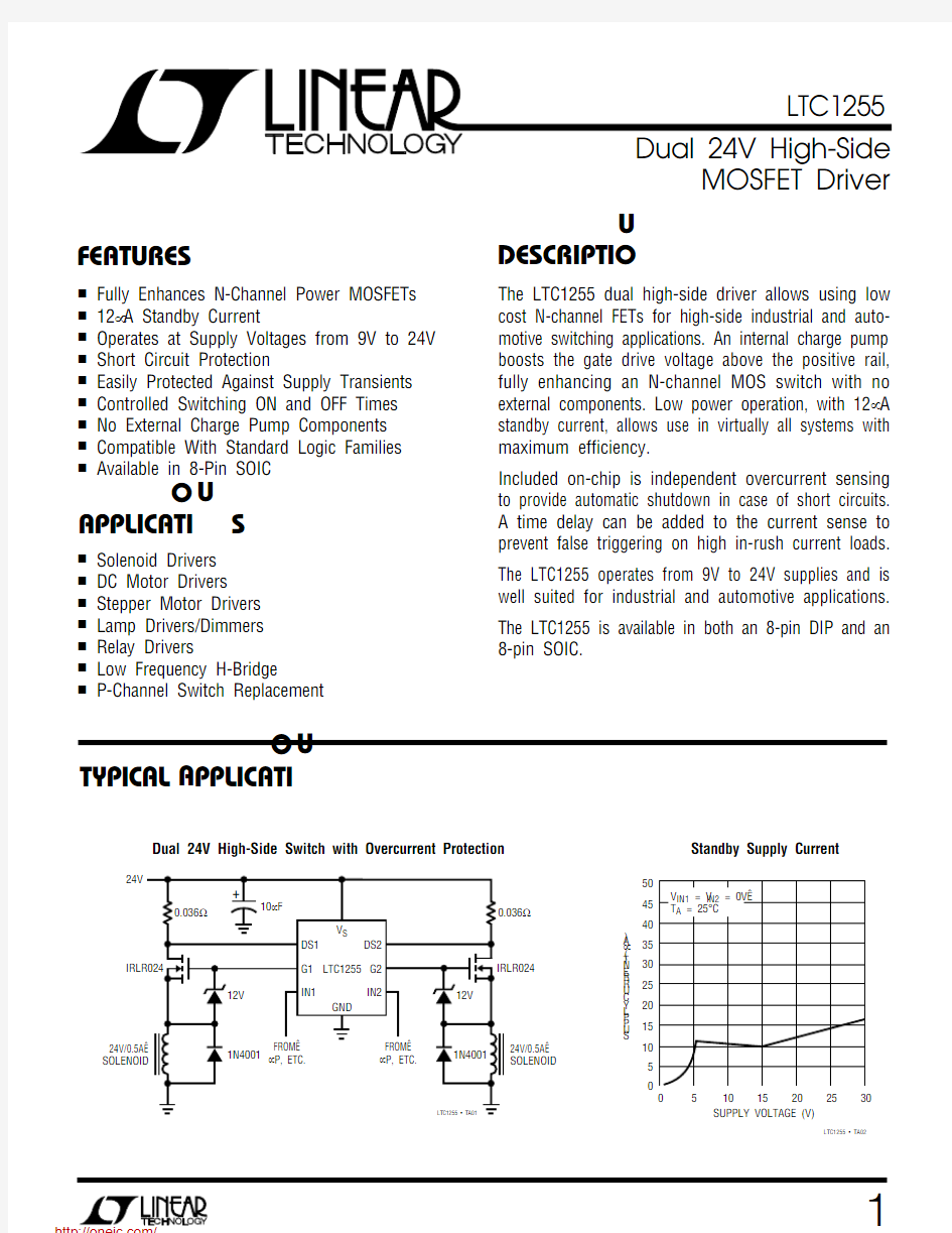
The LTC1255 dual high-side driver allows using low cost N-channel FETs for high-side industrial and auto-motive switching applications. An internal charge pump boosts the gate drive voltage above the positive rail,fully enhancing an N-channel MOS switch with no external components. Low power operation, with 12μA standby current, allows use in virtually all systems with maximum efficiency.
Included on-chip is independent overcurrent sensing to provide automatic shutdown in case of short circuits.A time delay can be added to the current sense to prevent false triggering on high in-rush current loads.The LTC1255 operates from 9V to 24V supplies and is well suited for industrial and automotive applications.The LTC1255 is available in both an 8-pin DIP and an 8-pin SOIC.
S
FEATURE s Fully Enhances N-Channel Power MOSFETs s 12μA Standby Current
s Operates at Supply Voltages from 9V to 24V s Short Circuit Protection
s Easily Protected Against Supply Transients s Controlled Switching ON and OFF Times s No External Charge Pump Components s Compatible With Standard Logic Families s
Available in 8-Pin SOIC
U S
A O
PPLICATI
s Solenoid Drivers s DC Motor Drivers s Stepper Motor Drivers s Lamp Drivers/Dimmers s Relay Drivers
s Low Frequency H-Bridge
s
P-Channel Switch Replacement
D U
ESCRIPTIO
U A O
PPLICATI
TYPICAL
24V
?
24V/0.5A SOLENOID
Standby Supply Current
Dual 24V High-Side Switch with Overcurrent Protection
SUPPLY VOLTAGE (V)
0S U P P L Y C U R R E N T (μA )
1015202530355
10
1520LTC1255 ? TA02
25
404550530
2
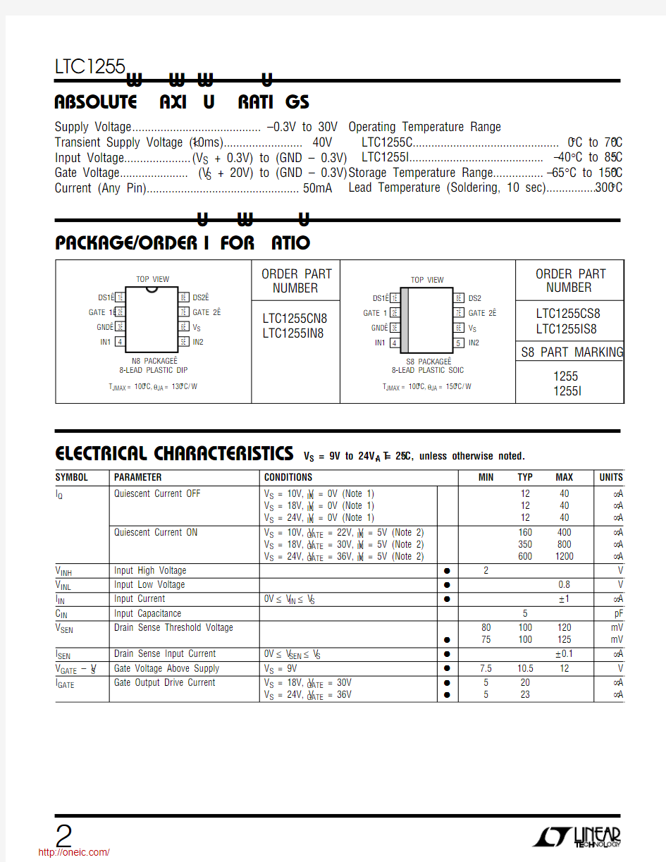
LTC1255Supply Voltage ......................................... –0.3V to 30V Transient Supply Voltage (<10ms)......................... 40V Input Voltage.....................(V S + 0.3V) to (GND – 0.3V)Gate Voltage ...................... (V S + 20V) to (GND – 0.3V)Current (Any Pin)................................................. 50mA
A U
G W
A W
U
W A R BSOLUTE
XI TI S
Operating Temperature Range
LTC1255C............................................... 0°C to 70°C LTC1255I........................................... –40°C to 85°C Storage Temperature Range................ –65°C to 150°C Lead Temperature (Soldering, 10 sec)................. 300°C
W
U
U
PACKAGE/ORDER I FOR ATIO
SYMBOL PARAMETER CONDITIONS
MIN
TYP MAX UNITS I Q
Quiescent Current OFF
V S = 10V, V IN = 0V (Note 1)1240μA V S = 18V, V IN = 0V (Note 1)1240μA V S = 24V, V IN = 0V (Note 1)
1240μA Quiescent Current ON
V S = 10V, V GATE = 22V, V IN = 5V (Note 2)160400μA V S = 18V, V GATE = 30V, V IN = 5V (Note 2)350800μA V S = 24V, V GATE = 36V, V IN = 5V (Note 2)
600
1200μA V INH Input High Voltage q 2
V V INL Input Low Voltage q
0.8V I IN Input Current 0V ≤ V IN ≤ V S
q
±1
μA C IN Input Capacitance
5pF V SEN Drain Sense Threshold Voltage 80100120mV q 75100125mV I SEN
Drain Sense Input Current 0V ≤ V SEN ≤ V S q ±0.1μA V GATE – V S Gate Voltage Above Supply V S = 9V
q 7.510.512
V I GATE
Gate Output Drive Current
V S = 18V, V GATE = 30V q 520μA V S = 24V, V GATE = 36V
q
5
23
μA
ELECTRICAL C C HARA TERISTICS
V S = 9V to 24V, T A = 25°C, unless otherwise noted.
https://www.doczj.com/doc/5110149293.html,/
3
LTC1255
SYMBOL PARAMETER CONDITIONS
MIN TYP MAX UNITS
t ON
Turn-ON Time
V S = 10V, C GATE = 1000pF (Note 3) Time for V GATE > V S + 2V 30100300μs Time for V GATE > V S + 5V
75250750μs V S = 18V, C GATE = 1000pF (Note 3) Time for V GATE > V S + 5V 40120400μs Time for V GATE > V S + 10V
75250750μs V S = 24V, C GATE = 1000pF (Note 3) Time for V GATE > V S + 10V
50180500μs t OFF
Turn-OFF Time
V S = 10V, C GATE = 1000pF, (Note 3, 4)102460μs V S
= 18V, C GATE = 1000pF, (Note 3, 4)102160μs V S = 24V, C GATE = 1000pF, (Note 3, 4)101960μs t SC
Short-Circuit Turn-OFF Time
V S = 10V, C GATE = 1000pF, (Note 3, 4)51630μs V S = 18V, C GATE = 1000pF, (Note 3, 4)51630μs V S = 24V, C GATE = 1000pF, (Note 3, 4)
5
16
30
μs
V S = 9V to 24V, T A = 25°C, unless otherwise noted.
ELECTRICAL C C HARA TERISTICS
The q denotes specifications which apply over the full operating temperature range.
Note 1: Quiescent current OFF is for both channels in OFF condition.
Note 2: Quiescent current ON is per driver and is measured independently.The gate voltage is clamped to 12V above the rail to simulate the effects of protection clamps connected across the GATE-SOURCE of the power MOSFET.
Note 3: Zener diode clamps must be connected across the GATE-SOURCE of the power MOSFET to limit V GS . 1N5242A (through hole) or
MMBZ5242A (surface mount) 12V Zener diodes are recommended. All Turn-ON and Turn-OFF tests are performed with a 12V Zener clamp in series with a small-signal diode connected between V S and the GATE output to simulate the effects of a 12V protection Zener clamp connected across the GATE-SOURCE of the power MOSFET.Note 4: Time for V GATE to drop below 1V.
C C HARA TERISTICS
U W
A TYPICAL PERFOR CE Standby Supply Current
Gate Voltage Above Supply
Supply Current per Driver (ON)
SUPPLY VOLTAGE (V)
00
V G A
T E – V S (V )
4681012145
10
1520LTC1255 ? TPC03
25161820230
SUPPLY VOLTAGE (V)
0S U P P L Y C U R R E N T (m A )
0.40.60.81.01.21.4
5
10
1520LTC1255 ? TPC0225
1.61.8
2.00.230
SUPPLY VOLTAGE (V)
0S U P P L Y C U R R E N T (μA )
1015202530355
10
1520LTC1255 ? TPC01
25
40
4550530
4
LTC1255
C C HARA TERISTICS
U W
A TYPICAL PERFOR CE Input Threshold Voltage
Short-Circuit Turn-OFF Delay Time
Turn-ON Time
Standby Supply Current
Supply Current per Channel (ON)
Input ON Threshold
Gate Clamp Current
Drain Sense Threshold Voltage
Turn-OFF Time
SUPPLY VOLTAGE (V)
0.4
I N P U T T H R E S H O L D V O L T A G E (V )
0.81.01.21.41.61.85
10
1520LTC1255 ? TPC04
25
2.0
2.22.4
0.6
30
SUPPLY VOLTAGE (V)
75D R A I N S E N S E T H R E S H O L D V O L T A G E (V )
8590951001051105
10
1520LTC1255 ? TPC0525
115
120125
8030
SUPPLY VOLTAGE (V)
0G A T E C L A M P C U R R E N T (μA )
1015202530355
10
1520LTC1255 ? TA06
25
404550530
SUPPLY VOLTAGE (V)
0T U R N -O N T I M E (μs )
2003004005006007005
10
1520LTC1255 ? TA0725
800
900100010030
SUPPLY VOLTAGE (V)
0T U R N -O F F T I M E (μs )
1015202530355
10
1520LTC1255 ? TA08
25
404550530
SUPPLY VOLTAGE (V)
00
T U R N -O F F T I M E (μs )
1015202530355
10
1520LTC1255 ? TA09
25404550530
TEMPERATURE (°C)
–50
0S T A N D B Y S U P P L Y C U R R E N T (μA )
101520253035–25
2550LTC1255 ? TA1075
4045505
100
TEMPERATURE (°C)
–50
0.4I N P U T T H R E S H O L D V O L T A G E (V )
0.81.01.21.41.61.8–25
2550LTC1255 ? TA12
752.02.22.40.6
100
TEMPERATURE (°C)
–50
0S U P P L Y C U R R E N T (m A )
0.40.60.81.01.21.4–25
2550LTC1255 ? TA1175
1.61.8
2.00.2
100
https://www.doczj.com/doc/5110149293.html,/
5
LTC1255
PI FU CTIO S
U
U U Input Pin
The LTC1255 input pin is active high and activates all of the protection and charge pump circuitry when switched ON. The LTC1255 logic and shutdown inputs are high impedance CMOS gates with ESD protection diodes to ground and supply and therefore should not be forced beyond the power supply rails. The input pin should be held low during the application of power to properly set the input latch.Gate Drive Pin
The gate drive pin is either driven to ground when the switch is turned OFF or driven above the supply rail when the switch is turned ON. This pin is of relatively high impedance when driven above the rail (the equiva-lent of a few hundred k ?). Care should be taken to minimize any loading of this pin by parasitic resistance to ground or supply.Supply Pin
The supply pin of the LTC1255 serves two vital pur-poses. The first is obvious; it powers the input, gate drive, regulation and protection circuitry. The second purpose is less obvious; it provides a Kelvin connection to the top of the drain sense resistor for the internal 100mV reference.
The supply pin of the LTC1255 should never be forced below ground as this may result in permanent damage to the device . A 100? resistor should be inserted in series with the ground pin if negative supply voltage transients are anticipated.
The LTC1255 is designed to be continuously powered so that the gate of the MOSFET is actively driven at all times. If it is necessary to remove power from the supply pin and then reapply it, the input pin should be cycled (low to high) a few milliseconds after the power is reapplied to reset the input latch and protection circuitry. Also, the input pin should be isolated from the controlling logic by a 10k resistor if there is a possibility that the input pin will be held high after the supply has been removed.Drain Sense Pin
The drain sense pin is compared against the supply pin voltage. If the voltage at this pin is more than 100mV below the supply pin, the input latch will be reset and the MOSFET gate will be quickly discharged. Cycle the input to reset the short-circuit latch and turn the MOSFET back on.
This pin is also a high impedance CMOS gate with ESD protection and therefore should not be forced outside of the power supply rails. To defeat the overcurrent protection, short the drain sense pin to the supply pin.Some loads, such as large supply capacitors, lamps or motors require high in-rush currents. An RC time delay can be added between the sense resistor and the drain sense pin to ensure that the drain sense circuitry does not false trigger during startup. This time constant can be set from a few microseconds to many seconds.However, very long delays may put the MOSFET at risk of being destroyed by a short-circuit condition (see Applications Information section).
OPERATIO
U
The LTC1255 is a dual 24V MOSFET driver with built-in protection and gate charge pump. The LTC1255 consists of the following functional blocks:
TTL and CMOS Compatible Inputs and Latches The LTC1255 inputs have been designed to accommo-date a wide range of logic families. Both input thresh-
olds are set at about 1.3V with approximately 100mV of hysteresis. A low standby current regulator provides continuous bias for the TTL-to-CMOS converter.The input/protection latch should be set after initial power-up, or after reapplication of power, by cycling the input low to high.
6
LTC1255
OPERATIO
U
Internal Voltage Regulation
The output of the TTL-to-CMOS converter drives two regulated supplies which power the low voltage CMOS logic and analog blocks. The regulator outputs are isolated from each other so that the noise generated by the charge pump logic is not coupled into the 100mV reference or the analog comparator.Gate Charge Pump
Gate drive for the power MOSFET is produced by an adaptive charge pump circuit which generates a gate voltage substantially higher than the power supply volt-age. The charge pump capacitors are included on-chip and therefore no external components are required to generate the gate drive. The charge pump is designed to drive a 12V Zener diode clamp connected across the gate and source of the MOSFET switch.
(One Channel)
BLOCK DIAGRA
W
Drain Current Sense
The LTC1255 is configured to sense the current flowing into the drain of the power MOSFET in a high-side applica-tion. An internal 100mV reference is compared to the drop across a sense resistor (typically 0.002? to 0.10?) in series with the drain lead. If the drop across this resistor exceeds the internal 100mV threshold, the input latch is reset and the gate is quickly discharged via a relatively large N-channel transistor.
Controlled Gate Rise and Fall Times
When the input is switched ON and OFF, the gate is charged by the internal charge pump and discharged in a controlled manner. The charge and discharge rates have been set to minimize RFI and EMI emissions in normal operation. If a short circuit or current overload condition is encountered, the gate is discharged very quickly (typi-cally a few microseconds) by a large N-channel transistor.
INPUT
https://www.doczj.com/doc/5110149293.html,/
7
LTC1255
APPLICATIO S I FOR ATIO
W U U U
MOSFET AND LOAD PROTECTION
The LTC1255 protects the power MOSFET switch by removing drive from the gate as soon as an overcurrent condition is detected. Resistive and inductive loads can be protected with no external time delay in series with the drain sense pin. Lamp loads, however, require that the overcurrent protection be delayed long enough to start the lamp but short enough to ensure the safety of the MOSFET.Resistive Loads
Loads that are primarily resistive should be protected with as short a delay as possible to minimize the amount of time that the MOSFET is subjected to an overload condition.The drain sense circuitry has a built-in delay of approxi-mately 10μs to eliminate false triggering by power supply or load transient conditions. This delay is sufficient to “mask” short load current transients and the starting of a small capacitor (<1μF) in parallel with the load. The drain sense pin can therefore be connected directly to the drain current sense resistor as shown in Figure 1.
18V
LOAD ?
SENSE ?
Figure 1. Protecting Resistive Loads
Inductive Loads
Loads that are primarily inductive, such as relays, sole-noids and stepper motor windings, should be protected with as short a delay as possible to minimize the amount of time that the MOSFET is subjected to an overload condition. The built-in 10μs delay will ensure that the overcurrent protection is not false triggered by a supply or load transient. No external delay components are required as shown in Figure 2.
Large inductive loads (>0.1mH) may require diodes con-nected directly across the inductor to safely divert the stored energy to ground. Many inductive loads have these diodes included. If not, a diode of the proper current rating should be connected across the load, as shown in Figure 2, to safely divert the stored energy.
Figure 2. Protecting Inductive Loads
Capacitive Loads
Large capacitive loads, such as complex electrical sys-tems with large bypass capacitors, should be powered using the circuit shown in Figure 3. The gate drive to the power MOSFET is passed through an RC delay network,R1 and C1, which greatly reduces the turn-on ramp rate of the switch. And since the MOSFET source voltage follows the gate voltage, the load is powered smoothly and slowly from ground. This dramatically reduces the startup cur-
rent flowing into the supply capacitor(s) which, in turn,reduces supply transients and allows for slower activation
Figure 3. Powering Large Capacitive Loads
12V
?
15V
?
LOAD μF
8
LTC1255
of sensitive electrical loads. (Resistor R2, and the diode D1, provide a direct path for the LTC1255 protection circuitry to quickly discharge the gate in the event of an overcurrent condition.)
The RC network, R DELAY and C DELAY , in series with the drain sense input should be set to trip based on the expected characteristics of the load after startup, i.e., with this circuit, it is possible to power a large capacitive load and still react quickly to an overcurrent condition. The ramp rate at the output of the switch as it lifts off ground is approximately:
dV/dt = (V GATE – V TH )/(R1 × C1)
Therefore, the current flowing into the capacitor during startup is approximately:I STARTUP = C LOAD × dV/dt
Using the values shown in Figure 3, the startup current is less than 100mA and does not false trigger the drain sense circuitry which is set at 2.7A with a 1ms https://www.doczj.com/doc/5110149293.html,mp Loads
The in-rush current created by a lamp during turn-on can be 10 to 20 times greater than the rated operating current.The circuit shown in Figure 4 shifts the current limit threshold up by a factor of 11:1 (to 30A) for a short period of time while the bulb is turned on. The current limit then drops down to 2.7A after the in-rush current has subsided.
APPLICATIO S I FOR ATIO
W U U U
12V
SENSE ?
12V/1A BULB
Figure 4. Lamp Driver With Delayed Protection
Selecting R DELAY and C DELAY
Figure 5 is a graph of normalized overcurrent shutdown
time versus normalized MOSFET current. This graph is used to select the two delay components, R DELAY and C DELAY , which make up a simple RC delay between the drain sense input and the drain sense resistor.The Y axis of the graph is normalized to one RC time constant. The X axis is normalized to the set current.(The set current is defined as the current required to develop 100mV across the drain sense resistor.)Note that the shutdown time is shorter for increasing levels of MOSFET current. This ensures that the total energy dissipated by the MOSFET is always within the bounds established by the manufacturer for safe opera-tion. (See MOSFET data sheet for further https://www.doczj.com/doc/5110149293.html,rmation.)
NORMALIZED MOSFET CURRENT (1 = SET CURRENT)
0.10.01
N O R M A L I Z E D D E L A Y T I M E (1 = R C )
0.1
1
10
110100LTC1255 ? F05
Figure 5. Normalized Delay Time vs MOSFET Current
Using a Speed-Up Diode
Another way to reduce the amount of time that the power MOSFET is in a short-circuit condition is to “bypass” the delay resistor with a small signal diode as shown in Figure 6. The diode will engage when the drop across the drain sense resistor exceeds about 0.7V,providing a direct path to the sense pin and dramatically reducing the amount of time the MOSFET is in an overload condition. The drain sense resistor value is selected to limit the maximum DC current to 4A.
https://www.doczj.com/doc/5110149293.html,/
9
LTC1255
APPLICATIO S I FOR ATIO
W U U U
18V
?
Figure 6. Using a Speed-Up Diode
The large output capacitors on many switching regula-tors, on the other hand, may be able to hold the supply pin of the LTC1255 above 3.5V sufficiently long that this extra filtering is not required.
Because the LTC1255 is micropower in both the standby and ON state, the voltage drop across the supply filter is very small (typically <6mV) and does not signifi-cantly alter the accuracy of the drain sense threshold voltage which is typically 100mV.AUTOMOTIVE APPLICATIONS Reverse Battery Protection
The LTC1255 can be protected against reverse battery conditions by connecting a resistor in series with the ground lead as shown in Figure 8. The resistor limits the supply current to less than 120mA with –12V applied.Since the LTC1255 draws very little current while in normal operation, the drop across the ground resistor is minimal. The 5V
μP (or controlling logic) is protected by the 10k resistors in series with the input.
Figure 7. Supply Filter for Current Limited Supplies
?
Figure 8. Reverse Battery Protection
Transient Overvoltage Protection
A common scheme used to limit overvoltage transients on a 14V nominal automotive power bus is to clamp the supply to the module containing the high-side MOSFET switches with a large transient suppressor diode, D1 in Figure 9. This diode limits the supply voltage to 40V under worse case conditions. The LTC1255 is designed to survive short (10ms) 40V transients and return to normal operation after the transient has passed.
Current Limited Power Supplies
The LTC1255 requires at least 3.5V at the supply pin to ensure proper operation. It is therefore necessary that the supply to the LTC1255 be held higher than 3.5V at all times, even when the output of the switch is short circuited to ground. The output voltage of a current limited regulator may drop very quickly during short circuit and pull the supply pin of the LTC1255 below 3.5V before the shutdown circuitry has had time to respond and remove drive from the gate of the power MOSFET. A supply filter should be added as shown in Figure 7 which holds the supply pin of the LTC1255high long enough for the overcurrent shutdown cir-cuitry to respond and fully discharge the gate.Linear regulators with small output capacitors are the most difficult to protect as they can “switch” from a voltage mode to a current limited mode very quickly.
15V
SENSE ?
10
LTC1255
The switches can either be turned OFF by the controlling logic during these transients or latched OFF above 30V by holding the drain sense pin low as shown in Figure 9.Switch status can be ascertained by means of an XNOR gate connected to the input and switch output through 100k current limiting resistors (see Typical Applications section for more detail on this scheme). The switch is reset after the overvoltage event by cycling the input low and then high again.
The power MOSFET switch should be selected to have a breakdown voltage sufficiently higher than the 40V supply clamp voltage to ensure that no current is conducted to the load during the transient.
APPLICATIO S I FOR ATIO
W U U U
Figure 9. Overvoltage Transient Protection
TYPICAL APPLICATIO S
U
Dual Automotive High-Side Switch with Overvoltage Protection,
XNOR Status and 12μA Standby Current
?
μ*OPTIONAL OVERVOLTAGE (30V) LATCH-OFF COMPONENTS
LIMITS V S TRANSIENTS TO <40V. SEE MANUFACTURER DATA SHEET FOR FURTHER DETAIL.
OPTIONAL OPEN LOAD DETECTION REQUIRES 10k PULL-UP RESISTORS. (ULTRA LOW STANDBY QUIESCENT CURRENT IS SACRIFICED) POWER FROM 5V LOGIC SUPPLY.
* ** ?
IN 0 1 0 1OUT 0 0 1 1CONDITION SWITCH OFF OVERCURRENT OPEN LOAD** SWITCH ON
FAULT 1 0 0 1
TRUTH TABLE https://www.doczj.com/doc/5110149293.html,/
分销商库存信息:
LINEAR-TECHNOLOGY
LTC1255CS8#PBF LTC1255CN8LTC1255CN8#PBF LTC1255CS8LTC1255CS8#TR LTC1255CS8#TRPBF LTC1255IN8LTC1255IS8LTC1255IS8#PBF LTC1255IS8#TR LTC1255IS8#TRPBF LTC1255IN8#PBF