GENERAL DESCRIPTION
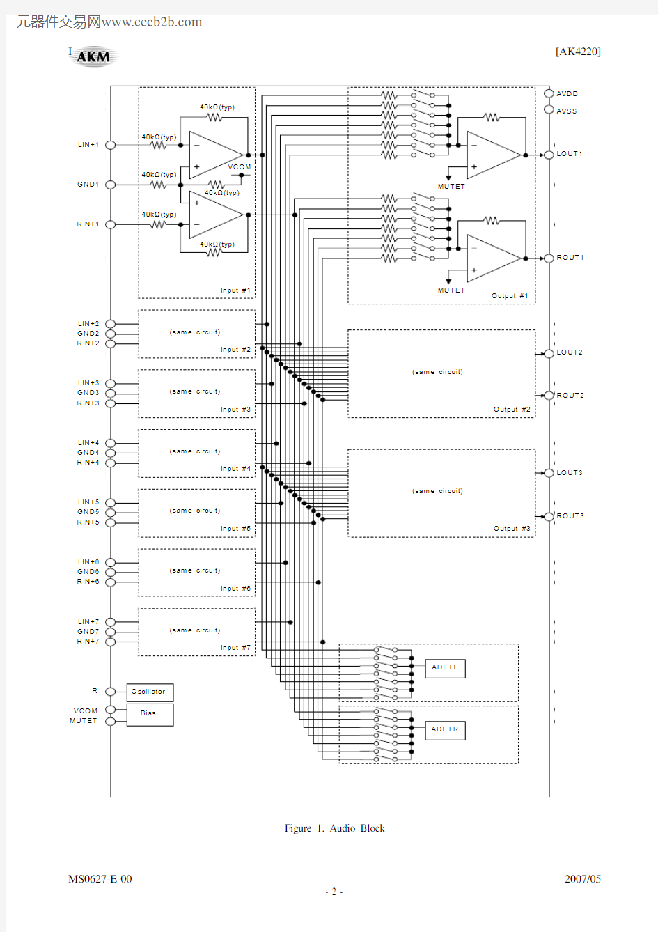
The AK4220 is an AV Switch with 7:3 Audio Switches and 6:3 Video Switches. Using CMOS process to offer the high performance with low power consumption. In the Audio section, on-chip differential input circuit could separate the external ground noise. The AK4220 integrates a pop noise free circuit for power on/pff. The AK4220 is offered in a space saving 64-pin LQFP package, ideal for car navigation applications.
FEATURES
1. Audio Section
? Selector for 7 inputs and 3 outputs
? Differential Input Circuit for Ground Noise Cannel ? THD+N: -92dB (@1Vrms) ? Dynamic Range: 96dB
? Channel-Independent Output Off
? Pop Noise Free Circuit for Power On/Off
? Channel-Independent Input Detection Circuit
2. Video Section
? Selector for 6 inputs and 3 outputs ? Six Composite Signal Inputs
? Video Driver for Composite Signal Output (+6dB) ? Channel-Independent Hi-Z Output ? On-Chip Sync-tip Clamp Circuit ? Frequency Range: 6MHz ? S/N: 74dB
? Input Detection Circuit
3. Control Section
? Serial μP I/F (I 2C, 4-wires serial) ? Five Programmable Output pins
4. Power Supply
? Analog: 4.5V ~ 5.5V ? Digital: 3.0V ~ 3.6V
? Low Power Consumption: 186mW
5. Ta = -40 ~ 85 °C
6. Package: 64pin LQFP
7:3 Audio Switch and 6:3 Video Switch
AK4220
AVD D
AVS S
LO U T 1
R O U T 1
LO U T 2
R O U T 2
LO U T 3
R O U T 3
LIN +1
G N D 1
R IN +1
LIN +2 G N D 2 R IN +2
LIN +3 G N D 3 R IN +3
LIN +4 G N D 4 R IN +4
LIN +5 G N D 5 R IN +5
LIN +6 G N D 6 R IN +6
LIN +7 G N D 7 R IN +7
R VC O M MU T ET
Figure 1. Audio Block
IICN SDA/CDTI SCL/CCLK
PDN CAD1/CSN CAD0/CDTO
TEST PDN
Figure 2. Video & Control Block
■ Ordering Guide
AK4220VQ ?40 ~ +85°C 64pin LQFP (0.5mm pitch)
AKD4220 Evaluation board for AK4220
■ Pin Layout
PIN/FUNCTION
No. Pin Name I/O Function 1 RIN+7 I Rch Audio Positive Input 7
2
PDN I
Power down Mode
“L”: Power down, Reset
“H”: Power up
The AK4220 should always be reset upon power-up.
CAD1 I Chip Address1 (IICN pin = “L”) 3
CSN I Chip Selector (IICN pin = “H”) SCL I Control Clock Input (IICN pin = “L”) 4
CCLK I Control Clock Input (IICN pin = “H”) SDA I/O Control Data Input/Output (IICN pin = “L”) 5
CDTI I Control Data Input (IICN pin = “H”) CAD0 I Chip Address0 (IICN pin = “L”) 6
CDTO O Control Data Output (IICN pin = “H”) 7 INT O Interrupt 8 Q0 O Parallel Output 0 (open drain output) 9 Q1 O Parallel Output 1 (open drain output) 10 Q2 O Parallel Output 2 (open drain output) 11 Q3 O Parallel Output 3 (open drain output) 12 Q4 O Parallel Output 4 (open drain output)
13 DVDD - Digital Power Supply
Normally connected to DVSS with a 0.1μF ceramic capacitor in parallel
with a 10μF electrolytic capacitor.
14 DVSS - Digital Ground 15 VOUT1 O Video Output 1 16 VFB1 I Video Feedback 1 17 TEST I Test pin, Connected to VVSS. 18 VOUT2 O Video Output 2 19 VFB2 I Video Feedback 2
20 VVDD2 - Video Power Supply, 5V
Normally connected to VVSS with a 0.1μF ceramic capacitor in parallel
with a 10μF electrolytic capacitor.
21 VOUT3 O Video Output 3 22 VFB3 I Video Feedback 3 23 VVSS2 - Video Ground2, 0V 24 VIN1 I Video Input 1 25 VVSS3 - Video Ground3, 0V 26 VIN2 I Video Input 2
27 VVDD1 - Video Power Supply, 5V
Normally connected to VVSS with a 0.1μF ceramic capacitor in parallel
with a 10μF electrolytic cap.
28 VIN3 I Video Input 3 29 VVSS1 - Video Ground1, 0V 30 VIN4 I Video Input 4
31 IICN I Control Mode Selection
“L”(Connected to VVSS): IIC Bus
“H” (Connected to VVDD): 4-wire Serial
32 VIN5 I Video Input 5 33 VIN6 I Video Input 6
34 AVDD - Audio Power Supply, 5V
Normally connected to AVSS with a 0.1μF ceramic capacitor in parallel
with a 10μF electrolytic capacitor.
PIN/FUNCTION (Continued)
35 R O Current Setting for Oscillator
Normally connected to AVSS with a 12k±1%Ωresistance.
36 MUTET O Audio Common Voltage Output2
Normally connected to AVSS with a 1μF ceramic capacitor.
37 VCOM O
Audio Common Voltage Output1 (Figure 3)
Normally connected to AVSS with a 0.1μF ceramic capacitor in parallel
with a 2.2
μF electrolytic capacitor.
38 AVSS - Audio Ground, 0V
39 LOUT1 O Lch Audio Output 1
40 ROUT1 O Rch Audio Output 1
41 LOUT2 O Lch Audio Output 2
42 ROUT2 O Rch Audio Output 2
43 LOUT3 O Lch Audio Output 3
44 ROUT3 O Rch Audio Output 3
45 GND1 I Audio Input Ground1
46 LIN+1 I Lch Audio Positive Input 1
47 RIN+1 I Rch Audio Positive Input 1
48 GND2 I Audio Input Ground 2
49 LIN+2 I Lch Audio Positive Input 2
50 RIN+2 I Rch Audio Positive Input 2
51 GND3 I Audio Input Ground 3
52 LIN+3 I Lch Audio Positive Input 3
53 RIN+3 I Rch Audio Positive Input 3
54 GND4 I Audio Input Ground 4
55 LIN+4 I Lch Audio Positive Input 4
56 RIN+4 I Rch Audio Positive Input 4
57 GND5 I Audio Input Ground 5
58 LIN+5 I Lch Audio Positive Input 5
59 RIN+5 I Rch Audio Positive Input 5
60 GND6 I Audio Input Ground 6
61 LIN+6 I Lch Audio Positive Input 6
62 RIN+6 I Rch Audio Positive Input 6
63 GND7 I Audio Input Ground 7
64 LIN+7 I Lch Audio Positive Input 7
Note: All digital input pins (PDN, CAD1-0, SCL and SDA pins) must not be left floating.
Figure 3. VCOM Circuit
■ Handling of Unused Pin
The unused I/O pins should be processed appropriately as below. Classification Pin
Name Setting
Analog LIN+1-LIN+7, RIN+1-RIN+7,
LOUT1-LOUT3,
ROUT1-ROUT3,VIN1-VIN6,
VOU1-VOUT3, VFB1-VFB3,
Q0-Q4, INT
These pins should be open.
Digital TEST These pins should be connected to DVSS.
ABSOLUTE MAXIMUM RATINGS
(AVSS = VVSS1-3 = DVSS = 0V; Note: 1)
Parameter Symbol
min
max
Units
Power Supplies Audio
Video
Video
Digital
|AVSS-DVSS| (Note: 2)
|AVSS-VVSS1| (Note: 2)
|AVSS-VVSS2| (Note: 2)
|AVSS-VVSS3| (Note: 2) AVDD
VVDD1
VVDD2
DVDD
ΔGND1
ΔGND2
ΔGND3
ΔGND4
-0.3
-0.3
-0.3
-0.3
-
-
-
6.0
6.0
6.0
6.0
0.3
0.3
0.3
0.3
V
V
V
V
V
V
V
V
Input Current (any pins except for supplies) IIN - ±10 mA
Audio Input Voltage
(LIN+1-7, RIN+1-7, GND1-7 pins) VINA -0.3 AVDD+0.3
V
Video Input Voltage1 (VIN1-6, IICN pins) VINV1 -0.3 VVDD1+0.3
V
Video Input Voltage2 (VFB1-3, TEST pins) VINV2 -0.3 VVDD2+0.3
V
Digital Input Voltage
(PDN, CAD1-0, SCL ,SDA pins) VIND -0.3 DVDD+0.3
V
Ambient Temperature (power applied) Ta -40 85 °C
Storage Temperature Tstg -65 150 °C
Note: 1. All voltages with respect to ground.
Note: 2. AVSS, VVSS1-3 and DVSS must be connected to the same analog ground plane.
WARNING: Operation at or beyond these limits may result in permanent damage to the device.
Normal operation is not guaranteed at these extremes.
RECOMMENDED OPERATING CONDITIONS
(AVSS = VVSS1-3 = DVSS = 0V; Note: 1)
Parameter Symbol
min
typ
max
Units
Power Supplies (Note: 3) Audio
Video (Note: 4)
Video (Note: 4)
Digital
VVDD1 – AVDD
VVDD2 – AVDD
AVDD
VVDD1
VVDD2
DVDD
ΔVDD1
ΔVDD2
4.5
4.5
4.5
3.0
-0.3
-0.3
5.0
5.0
5.0
3.3
5.5
5.5
5.5
3.6
+0.3
+0.3
V
V
V
V
V
V
Note: 3. The power-up sequence between AVDD, VVDD1, VVDD2 and DVDD is not critical. Note: 4. VVDD1 and VVDD2 must be the same voltage.
*AKEMD assumes no responsibility for the usage beyond the conditions in this datasheet.
ANALOG CHARACTERISTICS (AUDIO)
(Ta=25°C; AVDD = VVDD1-2 = 5V, DVDD =3.3V; AVSS = VVSS1-3 = DVSS = 0V; Signal Frequency=1kHz,
Measurement Frequency=20Hz~20kHz, unless otherwise specified)
Parameter min
typ
max
Units S/(N+D) Input=0dBV 82
92 dB
DR (0dBV) Input=-60dBV, A-weighted 88 96
dB
S/N (0dBV) Input=0ff, A-weighted 88 96 dB
Input Impedance (Note: 5)20 kΩ
Maximum Input Voltage (Note: 6) 1 - - Vrms
Gain -0.5
0.5
dB Interchannel Isolation (Note: 7) - 100 dB
Interchannel Gain Mismatch 0.2 - dB
Gain Drift 20 - ppm/°C
Load Resistance (Note: 8)R1+R2 (Figure 4) 5 kΩ
Load Capacitance C1 (Figure 4)
C2 (Figure 4) 400 30
pF
pF
Power Supply Rejection (Note: 9)- 50 dB Input Detection Circuit
Input Reception 1kHz (Note:
10) -43 -31 -26 dBV Input Reception Adjustment Gain Step (Note:
11) - 3 - dB Note: 5. Connected GND1-7 to GND using a capacitor for AC-coupling.
Note: 6. The Input Voltage meets S/(N+D)>82dB
Note: 7. Between all channels of LIN1-7 and RIN1-7.
Note: 8. The output resistance of audio output (LOUT1-3 and ROUT1-3) are less than l0Ω(typ).
Note: 9. Applied to AVDD, VVDD1-2 and DVDD with a sine wave (1kHz, 50mVpp).
Note: 10. Detect an instant value. 31dBV=+40mV0p. If the input voltage is smaller than the detection reception value, the signal isn’t detected, and if the input voltage is larger than the detection reception value, the signal is detected.
The input reception value is proportional to AVDD voltage as of 0.008 x AVDD V0p(typ).
Note: 11. Input Reception Adjustment Gain is +6dB~-6dB.
C2=C21+C22= 30pF(max) C1= 400pF(max)
Figure 4. Load Resistance R1, R2 and Load Capacitance C1, C2.
ANALOG CHARACTERISTICS (VIDEO)
(Ta=25°C; AVDD = VVDD1-2 = 5V, DVDD =3.3V; AVSS = VVSS1-3 = DVSS = 0V; unless otherwise specified)
Parameter Conditions
min typ
max
Units
Sync Tip Clamp Voltage
(Note: 12)
At output pin. - 0.6 - V
Gain (Note: 13) Input=0.3Vp-p, 100kHz 5.5 6 6.5 dB
Frequency Response (Note: 13)Input=0.3Vp-p, 100kHz to 6MHz. -1.0 1.0
dB
Maximum Input Signal f=100kHz, maximum with distortion < 1.0%,
gain=6dB(typ).
1.5 - - Vpp Load Resistance R1+R2(Note: 14) 150 - - Ω
Load Capacitance C1 (Note: 14)
C2 (Note: 14) 400 15
pF
pF Interchannel Isolation (Note: 15) f=4.43MHz, 1Vpp input. - 50 - dB
S/N Reference Level = 0.7Vpp, CCIR 567
weighting. BW= 15kHz to 5MHz.
- 74 - dB
Differential Gain 0.7Vpp 5steps modulated staircase.
chrominance &burst are 280mVpp, 4.43MHz.
- ±0.4 - %
Differential Phase 0.7Vpp 5steps modulated staircase.
chrominance &burst are 280mVpp, 4.43MHz.
- ±0.9 - Degree Input Detection Circuit
Input Reception (Note: 16) 0.040.07 0.1 Vpp Note: 12. SAGN bit=“1”, DC output. There is no specification for using the Sag Compensation circuit (SAGN bit=“0”).
Sync Tip Clamp Voltage is proportional to AVDD voltage, VOUT=0.17 x AVDD V(typ).
Note: 13. If SAGN bit=“0” for using the Sag Compensation circuit, the measurement point is between C3 and R1 of Figure 5. If SAGN bit=“1” for DC output, the measurement point is video output pin.
Note: 14. See Figure 5 and Figure 6.
Note: 15. Between all channels of VIN1-6.
Note: 16. If the input voltage is smaller than the detection reception value, the signal isn’t detected. If the input voltage is larger than the detection reception value, the signal is detected. The input reception value is proportional to
AVDD voltage, 0.014 x AVDD Vpp(typ).
C2=C21+C22+C23= 15pF(max)C1= 400pF(max)
Figure 5. Load Resistance R1, R2 and Load Capacitance C1, C2 (SAGN bit=“0”, using the Sag Compensation circuit)
C2=15pF(max)C1=400pF(max)
Figure 6. Load Resistance R1, R2 and Load Capacitance C1, C2 (SAGN bit=“1”, DC output)
DC CHARACTERISTICS
(Ta=-40~85°C; AVDD = VVDD1-2 = 4.5~5.5V, DVDD =3.0~3.6V)
Parameter Symbol min
typ
max
Units
High-Level Input Voltage
(PDN, SCL,SDA,CAD0-1,TEST,IICN pins) Low-Level Input Voltage
(PDN, SCL,SDA,CAD0-1,TEST,IICN pins)VIH
VIL
70%DVDD
-
-
-
-
30%DVDD
V
V
High-Level Output Voltage (Iout=-400μA)
Low-Level Output Voltage
(CDTO pin: Iout=400μA)
(Q0-4, INT pins: Iout=1mA)
(SDA pin: Iout=3mA)VOH
VOL
VOL
VOL
DVDD-0.4
-
-
-
-
-
-
-
-
0.4
0.4
0.4
V
V
V
V
Input Leakage Current Iin - - ±10 μA
Parameter min
typ
max
Units Power Supplies
Power Supply Current
Normal Operation (PDN pin = “H”) (Note: 17)
AVDD
VVDD1+VVDD2 (Note: 18) DVDD
Power-down mode (PDN pin = “L”) (Note: 19) AVDD
VVDD1+VVDD2
DVDD
Total 18
18
1
10
10
10
30
27
27
2
50
mA
mA
mA
μA
μA
μA
μA
Note: 17. No input and no load.
Note: 18. If the output is DC output (SAGN bit =“1”), the current corresponded to the load resistance is added to no load current (typ. 18mA).
Note: 19. All analog input pins are no input, and all digital input pins are fixed to DVSS.
SWITCHING CHARACTERISTICS (Ta= -40~85°C; AVDD = VVDD1-2 = 4.5~5.5V, DVDD= 3.0~3.6V, C L= 20pF) Control Interface Timing (I2C Bus, Note: 20)
SCL Clock Frequency
Bus Free Time Between Transmissions
Start Condition Hold Time (prior to first clock pulse) Clock Low Time
Clock High Time
Setup Time for Repeated Start Condition
SDA Hold Time from SCL Falling (Note: 21) SDA Setup Time from SCL Rising
Rise Time of Both SDA and SCL Lines
Fall Time of Both SDA and SCL Lines
Setup Time for Stop Condition
Pulse Width of Spike Noise Suppressed by Input Filter Capacitive load on bus fSCL
tBUF
tHD:STA
tLOW
tHIGH
tSU:STA
tHD:DAT
tSU:DAT
tR
tF
tSU:STO
tSP
Cb
-
1.3
0.6
1.3
0.6
0.6
0.1
-
-
0.6
-
400
-
-
-
-
-
-
-
0.3
0.3
-
50
400
kHz
μs
μs
μs
μs
μs
μs
μs
μs
μs
μs
ns
pF
Control Interface Timing (4-wire serial mode)
CCLK Period
CCLK Pulse Width Low Pulse Width High CDTI Setup Time CDTI Hold Time
CSN “H” Time
CSN “↓” to CCLK “↑” CCLK “↑” to CSN “↑” CDTO Delay
CSN “↑” to CDTO Hi-Z tCCK
tCCKL
tCCKH
tCDS
tCDH
tCSW
tCSS
tCSH
tDCD
tCCZ
200
80
80
50
50
150
50
50
45
70
ns
ns
ns
ns
ns
ns
ns
ns
ns
ns
Power-down & Reset Timing
PDN Pulse Width (Note: 21) TPD 150 ns Note: 20. I2C is a registered trademark of Philips Semiconductors.
Note: 21. Data must be held for sufficient time to bridge the 300 ns transition time of SCL.
Note: 22. The AK4220 should be reset by PDN pin = “L” upon power up.
■ Timing Diagram
VIH
VIL
VIH
VIL
Figure 7. I 2
C Bus Mode Timing
CSN
CCLK
CDTI CDTO
Hi-Z
VIH VIL
VIH VIL
VIH
VIL
Figure 8. WRITE/READ Command Input Timing (4-wire serial mode)
CSN
CCLK
CDTI D2D0
CDTO
Hi-Z
D1D3VIH VIL VIH VIL
VIH
VIL
Figure 9. WRITE Data Input Timing (4-wire serial mode)
CSN
CCLK
CDTO
CDTI VIH VIL
VIH VIL
VIH
VIL
Figure 10. READ Data Output Timing1 (4-wire serial mode)
CSN
CCLK
CDTO CDTI
VIH VIL VIH VIL
VIH VIL
Figure 11. READ Data Output Timing2 (4-wire serial mode)
PDN
VIL
Figure 12. Power-down & Reset Timing
OPERATION OVERVIEW
■Power-down options
The AK4220 should be reset once by bringing PDN pin = “L” upon power-up.
■ Audio Bias Control Circuit
The AK4220 has an on-chip audio bias voltage control circuit. Bringing BIAS bit to “1”, the bias voltage (MUTET pin) smoothly set from AVSS to AVDD/2(typ) by 150ms (typ, Note: 23). The change of BIAS bit from “1” to “0” also makes smooth transient from AVDD/2(typ) to AVSS by 150ms (typ, Note: 23). This feature achieves pop noise free at power-on/off.
Note: 23. AVDD=5.0V, the capacitor of MUTET pin is C=1uF. The rise and fall times are proportional to the voltage of AVDD and the capacitor value of MUTET pin.
PDN pin
BIAS bit
Figure 13. BIAS bit
■ Audio Signal Input, Video Signal Input
1. Audio Signal Input
The ground noise can be cancelled by the differential input with the same ground for L and R channel. The output of LIN and RIN are the same phase. LIN+1-7, RIN+1-7 and GND1-7 pins must be AC coupled using 0.47uF capacitor.
2. Video Signal Input
Tip Sync level is fixed by internal clamp circuit. VIN1-6 pins must be input through 0.47uF capacitor for AC coupling.
■ Input Selector
The AK4220 have 7:3 input selectors for audio input, and 6:3 input selectors for video input. The audio input selectors are set by ASEL12-10bits, ASEL22-20bits and ASEL32-30 bits, and the video input selectors are set by VSEL12-10bits, VSEL22-20bits and VSEL32-30 bits.
ASEL12 bit ASEL11 bit ASEL10 bit Input Selector
(Note: 24) (default)
Off
0 0 0
0 0 1 LIN1 / RIN1
0 1 0 LIN2 / RIN2
0 1 1 LIN3 / RIN3
1 0 0 LIN4 / RIN4
1 0 1 LIN5 / RIN5
1 1 0 LIN6 / RIN6
1 1 1 LIN7 / RIN7
Table 1. Audio Input Selector 1 (LOUT1/ROUT1)
ASEL22 bit ASEL21 bit ASEL20 bit Input Selector
(Note: 24) (default)
Off
0 0 0
0 0 1 LIN1 / RIN1
0 1 0 LIN2 / RIN2
0 1 1 LIN3 / RIN3
1 0 0 LIN4 / RIN4
1 0 1 LIN5 / RIN5
1 1 0 LIN6 / RIN6
1 1 1 LIN7 / RIN7
Table 2. Audio Input Selector 2 (LOUT2/ROUT2)
ASEL32 bit ASEL31 bit ASEL30 bit Input Selector
Off
(Note: 24) (default)
0 0 0
RIN1
/
0 0 1
LIN1
/
RIN2
LIN2
0 1 0
RIN3
/
LIN3
0 1 1
RIN4
/
LIN4
1 0 0
/
RIN5
LIN5
1 0 1
RIN6
/
LIN6
1 1 0
RIN7
/
1 1 1
LIN7
Table 3. Audio Input Selector 3 (LOUT3/ROUT3)
Note: 24. The audio outputs become common voltage (VCOM) when the input selectors are off. If BIAS bit = “0”, the outputs become 0V.
VSEL12 bit VSEL11 bit VSEL10 bit Input Selector
Off
(Note: 25) (default)
0 0 0
0 0 1 VIN1
0 1 0 VIN2
0 1 1 VIN3
1 0 0 VIN4
1 0 1 VIN5
1 1 0 VIN6
1 1 1 N/A
Table 4. Video Input Selector 1 (VOUT1)
VSEL22 bit VSEL21 bit VSEL20 bit Input Selector
(Note: 25) (default)
0 0 0
Off
0 0 1 VIN1
0 1 0 VIN2
0 1 1 VIN3
1 0 0 VIN4
1 0 1 VIN5
1 1 0 VIN6
1 1 1 N/A
Table 5. Video Input Selector 2 (VOUT2)
VSEL32 bit VSEL31 bit VSEL30 bit Input Selector
Off
(Note: 25) (default)
0 0 0
0 0 1 VIN1
0 1 0 VIN2
0 1 1 VIN3
1 0 0 VIN4
1 0 1 VIN5
1 1 0 VIN6
1 1 1 N/A
Table 6. Video Input Selector 3 (VOUT3)
Note: 25. The video outputs become Hi-Z when the input selectors are off.
■ Input Detection Circuit, INT pin Output
The AK4220 has channel-independent audio input detection circuit and video synchronization signal detection circuit. Each input source is set as shown in Table 7 and Table 8.
ADSEL2 bit ADSEL1 bit ADSEL0 bit Detection Source
0 0 0 Off (default) 0 0 1 LIN1 / RIN1 0 1 0 LIN2 / RIN2 0 1 1 LIN3 / RIN3 1 0 0 LIN4 / RIN4 1 0 1 LIN5 / RIN5 1 1 0 LIN6 / RIN6 1 1 1 LIN7 / RIN7
Table 7. Audio Input Detection Selector
VDSEL2 bit VDSEL1 bit VDSEL0 bit Detection Source
0 0 0 Off (default) 0 0 1 VIN1 0 1 0 VIN2 0 1 1 VIN3 1 0 0 VIN4 1 0 1 VIN5 1 1 0 VIN6 1 1 1 N/A
Table 8. Video Synchronization Signal Detection Selector
1. ADETL bit (Lch Audio Input Detection), ADETR bit (Rch Audio Input Detection)
The audio input detection circuit samples the input signal by accuracy of 100kHz ±30%.
If the signal over the detection reception value is detected consecutively more than the frequency set by ACT1-0 bits, ADETL-R bits become “1” and if the signal over the detection reception value isn’t detected consecutively more than the frequency set by ACT1-0 bits during the time set by RTM1-0 bit, ADETL-R bits become “0”.
The audio input detection for L/R channels is done independently. The input reception can be adjusted in the range of ±6dB from -31dBV(= +40mV 0p)(typ) by LV2-0 bits. When writing to 05H(ADSEL2-0, ACT1-0, RTMI1-0 bits), the counters for the consecutive detection frequency and recovery time are reset, and ADETL/R bits are reset to “0”.
The setting of MADEL/R bit doesn’t affect the operation of ADETL/R bit.
LV2 bit LV1 bit LV0 bit Input Reception
0 0 0 -6dB 0 0 1 -3dB 0 1 0 0dB (default) 0 1 1 +3dB 1 0 0 +6dB 1 0 1 N/A 1 1 0 N/A 1 1 1 N/A
0dB = +40mV 0p(typ)
Table 9. Level Setting of Audio Input Detection
ACT1 bit ACT0 bit Consecutive Detect Frequency
0 0 1 (default) 0 1 2 1 0 4 1 1 8
Table 10. Consecutive Detection frequency Setting of Audio Input Detection
RTM1 bit
RTM0 bit
Recovery Time
(typ)
0 0 40ms 0 1 80ms (default) 1 0 160ms 1 1 320ms
Table 11. Recovery Time Setting of Audio Input Detection
INT pin
ADETL bit
Input pin (ex. LIN+1)
Figure 14. Audio Detection Operation
2. VDET bit (Video Sync Signal Detection)
The video sync signal detection circuit can change the detection mode by VDMD bit.
VDMD bit =“0” (default)
When video sync signal above 0.07Vpp(typ) is detected, VDET bit become “1” and VDET bit returns to “0” after reading the register of 08H. The VDET bit is also reset to “0” by writing to the register of 04H with VDSEL2-0 bits.
When writing to 04H(VDSEL2-0 bits) the VDET bit become “0”.
VDMD bit =“1”
The detection circuit counts the number of video sync signal above 0.07Vpp(typ) every 40ms(±30%) period generated by the internal counter. When the period with the sync of 384 or more continues tow times, the VDET bit becomes “1” after 1/2 period. When the period with the sync signal less than 384 continues tow times, the VDET bit becomes “0” after 1/2 period.
The internal timer isn’t reset when changing the input source. Therefore the detection time, from after changing the input source to VDET bit = “1”, depends on the timing of input source change.
In case of a period that the internal timer count is the shortest(40ms x 70% = 28ms), when the detection circuit counts 384 times during the first period that receives video sync signal and counts 384 times or more in the following period, the detection time becomes the shortest.
Detection time (min) = (1/fH) x 384 + 28ms x 1.5 ? 66.6ms @ fH=15.625kHz
fH: frequency of video synchronization signal
If a period that internal timer counts is the longest (40ms x 130% = 52ms), when the detection circuit counts only 383 times during the first period that receives video sync signal and counts 384 times or more in the following two periods, the detection time becomes the longest.
Detection time (max) = (1/fH) x 384 + 52ms x 2.5 ? 154.5ms @ fH=15.625kHz
fH: frequency of video synchronization signal
When writing to 04H(VDSEL2-0bits), the internal timer is reset and VDET bit becomes “0”.
The setting of MVDET bit doesn’t affect the operation of VDET bit.
Input pin
(ex. VIN1)
384 times384 times
VDET bit
Input pin
(ex. VIN1)
384 times384 times
VDET bit
3. INT pin output
The output source of INT pin is ORed between ADETL/R bits and VDET bit If the output source of INT pin is “H”, INT pin=“L”, and if the output source of INT pin is “L”, INT pin=“Hi-Z”. If each mask bit is “1”, each detection bit is masked independently and the detection result isn’t reflected to INT pin.
Figure 16. INT Pin Output
MVDET bit MADETL bit MADETR bit INT pin output source
0 0 0 “OR” (VDET bit, ADETL bit, ADETR bit) (default)
0 0 1 “OR” (VDET bit , ADETL bit)
0 1 0 “OR” (VDET bit, ADETR bit)
0 1 1 VDET
bit
1 0 0 “OR” (ADETL bit, ADETR bit)
bit
1 0 1 ADETL
bit
1 1 0 ADETR
1 1 1 “L”(INT pin = “Hi-Z”)
Table 12. INT Pin Output Setting