High Dynamic Four Quadrant Switched Reluctance Drive Based on DITC
- 格式:pdf
- 大小:1.70 MB
- 文档页数:11

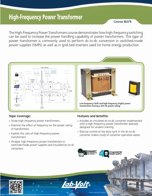
Course 86378The High-Frequency Power Transformers course demonstrates how high-frequency switching can be used to increase the power handling capability of power transformers. This type of power transformer is commonly used to perform dc-to-dc conversion in switched-mode power supplies (SMPS) as well as in grid-tied inverters used for home energy production.Topic Coverage:»Study high-frequency power transformers.»Examine the effect of frequency on the power rating of transformers.»Explore the uses of high-frequency power transformers.»Analyze high-frequency power transformers in switched-mode power supplies and insulated dc-to-dc converters.Features and Benefi ts:»Includes an insulated dc-to-dc converter implemented with a high-frequency power transformer specially designed for student training.»Manual control of the duty cycle in the dc-to-dc converter makes study of converter operation easier.4DYNAMOMETERPOWER SUPPLYOLow-frequency (left) and high-frequency (right) power transformers having a 250 VA power rating.QtyModelDescription18131Three-Module Workstation 18311Resistive Load18835Insulated DC-to-DC Converter 18951-L Connection Leads18960-CFour-Quadrant Dynamometer/Power SupplyQtyModelDescription19063-C Data Acquisition and Control Interface 130004-224 V AC Power Supply186378/-1Student Manual/Instructor GuideLab-Volt reserves the right to make product improvements at any time and without notice.Note: A computer is required to perform the exercises.。
轨道交通学院毕业设计(论文)外文翻译题目:列车车载的直流恒流源的设计专业电子信息工程班级10115111学号1011511137姓名赵士伟指导教师陈文2014 年3 月 3 日本文摘自:IEEE TRANSACTIONS ON INDUSTRY AND GENERAL APPLICATIONS VOL. IGA-2, NO.5 SEPT/OCT 1966Highly Regulated DC Power Supplies Abstract-The design and application of highly regulated dc power supplies present many subtle, diverse, and interesting problems. This paper discusses some of these problems (especially inconnection with medium power units) but emphasis has been placed more on circuit economics rather than on ultimate performance.Sophisticated methods and problems encountered in connection with precision reference supplies are therefore excluded. The problems discussed include the subjects of temperature coefficient,short-term drift, thermal drift, transient response degeneration caused by remote sensing, and switching preregualtor-type units and some of their performance characteristics.INTRODUCTIONANY SURVEY of the commercial de power supply field will uncover the fact that 0.01 percent regulated power supplies are standard types and can be obtained at relatively low costs. While most users of these power supplies do not require such high regulation, they never-theless get this at little extra cost for the simple reason that it costs the manufacturer very little to give him 0.01 percent instead of 0.1 percent. The performance of a power supply, however, includes other factors besides line and load regulation. This paper will discuss a few of these-namely, temperature coefficient, short-term drift, thermal drift, and transient response. Present medium power dc supplies commonly employ preregulation as a means of improving power/volume ratios and costs, but some characteristics of the power supply suffer by this approach. Some of the short-comings as well as advantages of this technology will be examined.TEMPERATURE COEFFICIENTA decade ago, most commercial power supplies were made to regulation specifications of 0.25 to 1 percent. The reference elements were gas diodes having temperature coefficients of the order of 0.01 percent [1]. Consequently, the TC (temperature coefficient) of the supply was small compared to the regulation specifications and often ignored. Today, the reference element often carries aTC specification greater than the regulation specification.While the latter may be improved considerably at little cost increase, this is not necessarily true of TC. Therefore,the use of very low TC zener diodes, matched differential amplifier stages, and low TC wire wound resistors must be analyzed carefully, if costs are to be kept low.A typical first amplifier stage is shown in Fig. 1. CRI is the reference zener diode and R, is the output adjustment potentiometer.Fig. 1. Input stage of power supply.Fig. 2. Equivalent circuit of zener reference.Let it be assumed that e3, the output of the stage, feedsadditional differential amplifiers, and under steady-state conditions e3 = 0. A variation of any of the parameters could cause the output to drift; while this is also true of the other stages, the effects are reduced by the gain of all previous stages. Consequently, the effects of other stages will be neglected. The following disculssion covers the effects of all elements having primary and secondary influences on the overall TC.Effect of R3The equivalent circuit of CRI -R3 branch is shown in Fig. 2. The zener ha's been replaced with its equivalent voltage source E/' and internal impedance R,. For high gain regulators, the input of the differential amplifier will have negligible change with variations of R3 so thatbefore and after a variation of R3 is made.If it is further assumed that IB << Iz; then from (1)Also,Eliminating I, from (2b),andNow, assuming thatthen,Equation (2b) can also be writtenThe Zener DiodeThe zener diode itself has a temperature coefficient andusually is the component that dominates the overall TCof the unit. For the circuit of Fig. 1, the TC ofthe circuit describes, in essence, the portion of the regulator TC contributed by the zener. If the bridge circuit shown in Fig. 1 were used in conjunction with a dropping resistor so that only a portion of the output voltage appeared across the bridge circuit shown, the TC of the unit and the zener would be different. Since the characteristic of zeners is so well known and so well described in the literature, a discussion will not be given here [2].Variation of Base-Emitter VoltagesNot only do the values of V,, of the differential am-plifier fail to match, but their differentials with tem perature also fail to match. This should not, however,suggest that matched pairs are required. The true reference voltage of Fig. 1 is not the value E,, but E, + (Vie, -Vbe2)-Since, for most practical applicatioinsthe TC of the reference will be the TC of the zener plusConsidering that it is difficult to obtain matched pairs that have differentials as poor as 50 V/°C, it becomes rather apparent that, in most cases, a matched pair bought specifically for TC may be overdesigning.Example 2: A standard available low-cost matched pair laims 30AV/°C. In conjunction with a 1N752, the ontribution to the overall TC would beTests, performed by the author on thirteen standard germanium signal transistors in the vicinity of room temperature and at a collector current level of 3 mA,indicated that it is reasonable to expect that 90 to 95 percent of the units would have a base-emitter voltage variation of -2.1 to -2.4 mV/°C. Spreads of this magnitude have also been verified by others (e.g., Steiger[3]). The worst matching of transistors led to less than 400 ,V/°C differential. In conjunction with a 1N752,even this would give a TC of better than 0.007%/0C.Variation of Base CurrentsThe base current of the transistors is given byA variation of this current causes a variation in signal voltage at the input to the differential amplifier due to finite source impedances. Matching source impedances is not particularly desirable, since it reduces the gain of the system and requires that transistors matched for I,o and A be used. Hunter [4 ] states that the TC of a is in the range of +0.2%/0C to -0.2%7/'C and that 1,, may be approximated bywhere Ao is the value at To.β is also temperature dependent and Steiger [3] experimentally determined the variation to be from about 0.5%/°C to 0.9%/0C.And,Fig. 3. Input circuit of Q2.The current AIB flows through the source impedance per Fig. 3. The drops in the resistance string, however, are subject to the constraint that EB (and AEB) are determined by the zener voltage and the base-emitter drops of Q1 and Q2. Consequently, if in going from temperature T1to T2 a change AEB occurs,The change in output voltage isAndExample 3: For Q2 (at 25°C)(see Example 1)∴Variation of R,The effects of a variation of the TC between RIA and RIB is sufficiently self-evident so that a discussion of the contribution is not included.SHORT-TERM DRIFTThe short-term drift of a supply is defined by the National Electrical Manufacturers Association (NEMA) as "a change in output over a period of time, which change is unrelated to input, environment, or load [5]."Much of the material described in the section on temperature coefficient is applicable here as well. It has been determined experimentally, however, that thermal air drafts in and near thevicinity ofthe powersupplycontributesenormouslyto theshort-termcharacteristics. Thecooling effects of moving air are quite well known, but it is not often recognized that even extremely slow air movements over such devices as zeners and transistors cause the junction temperature of these devices to change rapidly. If the TC of the supply is large compared to the regulation, then large variations in the output will be observed. Units having low TC's achieved by compensation-that is, by canceling out the effects of some omponents by equal and opposite effects of others may still be plagued by these drafts due to the difference in thermal time constants of the elements.Oftentimes, a matched transistor differential amplifier in a common envelope is used for the first amplifier just to equalize and eliminate the difference in cooling effects between the junctions. Approximations to this method include cementing or holding the transistors together, imbedding the transistors in a common metal block, etc. Excellent results were achieved by the author by placing the input stage and zener reference in a separate enclosure. This construction is shown in Fig. 4. The improvement in drift obtained by means of the addition of the metal cover is demonstrated dramatically in Fig. 5.Fig. 5. Short-term drift of a power supply similar to the one shown in Fig. 4 with and without protective covers. The unit was operated without the cover until time tl, when the cover was attached. The initial voltage change following t, is due to a temperaturerise inside the box.Fig. 5. Short-term drift of a power supply similar to the one shown n Fig. 4 withand without protective covers. The unit was operated without the cover until time tl, when the cover was attached. The initial voltage change following t, is due to atemperature rise inside the box.If potentiometers are used in the supply for output adjustment (e.g., RI), care should be used in choosing the value and design. Variations of the contact resistance can cause drift. It is not always necessary, however, to resort to the expense of high-resolution multiturn precision units to obtain low drift. A reduction in range of adjustment, use of low-resistance alloys and low-resolution units which permit the contact arm to rest firmly between turns, may be just as satisfactory. Of course, other considerations should include the ability of both the arms and the wire to resist corrosion. Silicone greases are helpful here. Periodic movement of contact arms has been found helpful in "healing" corroded elements.THERMAL DRIFTNEMA defines thermal drift as "a change in output over a period of time, due to changes in internal ambient temperatures not normally related to environmental changes. Thermal drift is usually associated with changes in line voltage and/or load changes [5]."Thermal drift, therefore, is strongly related to the TC of the supply as well as its overall thermal design. By proper placement of critical components it is possible to greatly reduce or even eliminate the effect entirely. It is not uncommon for supplies of the 0.01 percent(regulation) variety to have drifts of between 0.05 to 0.15 percent for full line or full load variations. In fact, one manufacturer has suggested that anything better than 0.15 percent is good. Solutions to reducing thermal drift other than the obvious approach of improving the TC and reducing internal losses include a mechanical design that sets up a physical and thermal barrier between the critical amplifier components and heat dissipating elements. Exposure to outside surfaces with good ventilation is recommended. With care, 0.01 to 0.05 percent is obtainable.TRANSIENT RESPONSEMost power supplies of the type being discussed have a capacitor across the load terminals. This is used for stabilization purposes and usually determines the dominant time constant of the supply. The presence of this capacitor unfortunately leads to undesirable transient phenomena when the supply is used in the remote sensing mode①. Normally, transistorized power supplies respond in microseconds, but as the author has pointed out [6], the response can degenerate severely in remote sensing .The equivalent circuit is shown in Fig. 6. The leads from the power supply to the load introduce resistance r. Is is the sensing current of the supply and is relatively constant.Under equilibrium conditions,A sudden load change will produce the transient of Fig. 7. The initial "spike" is caused by an inductive surge Ldi/dt; the longer linear discharge following is the resultof the capacitor trying to discharge (or charge). The discharge time iswhereandThe limitations of I,, are usually not due to available drive of the final amplifier stages but to other limitations, current limiting being the most common. Units using pre regulators of the switching type (transistor or SCR types) should be looked at carefully if the characteristics mentioned represent a problem.①Remote sensing is the process by which the power supply senses voltage directly at the load.Fig. 6. Output equivalent circuit at remote sensing.Fig. 7. Transient response, remote sensing.Fig. 8. Block diagram.Preregulated supplies are used to reduce size and losses by monitoring and controlling the voltage across the class-A-type series passing stage (Fig. 8). Since the main regulator invariably responds much quicker than the preregulator, sufficient reserve should always be built into the drop across the passing stage. Failure to provide this may result in saturation of the passing stage when load is applied, resulting in a response time which is that of the preregulator itself.SWITCHING PREREGULATOR-TYPE UNITS The conventional class-A-type transistorized power supply becomes rather bulky, expensive, and crowded with passing stages, as the current and power level of the supply increases. The requirement of wide output adjustment range, coupled with the ability of the supply to be remotely programmable, aggravates the condition enormously. For these reasons the high-efficiency switching regulator has been employed as a preregulator in commercial as well as military supplies for many years. The overwhelming majority of the supplies used silicon controlled rectifiers as the control element. For systems operating from 60-cycle sources, this preregulator responds in 20 to 50 ms.Recent improvements in high-voltage, high-power switching transistors has made the switching transistor pproach more attractive. This system offers a somewhat lower-cost, lower-volume approach coupled with a submillisecond response time. This is brought about by a high switching rate that is normally independent of line frequency. The switching frequency may be fixed, a controlled variable or an independent self-generated (by the LC filter circuit) parameter [7], [8]. Faster response time is highly desirable since it reduces the amount of reserve voltage required across the passing stage or the amount of (storage) capacity required in the preregulator filter.A transistor suitable for operating as a power switch has a high-current, high-voltage rating coupled with low leakage current. Unfortunately, these characteristics are achieved by a sacrifice in thermal capacity, so that simultaneous conditions of voltage and current leading to high peak power could be disastrous. It therefore becomes mandatory to design for sufficient switch drive during peak load conditions and also incorporate current-limiting or rapid overload protection systems.Commercial wide-range power supplies invariably have output current limiting, but this does not limit the preregulator currents except during steady-state load conditions (including short circuits). Consider, for example, a power supply operating at short circuit and the short being removed suddenly. Referring to Fig. 8, the output would rise rapidly, reduce the passing stage voltage, and close the switching transistor. The resulting transient extends over many cycles (switching rate) so that the inductance of the preregulator filter becomes totally inadequate to limit current flow. Therefore, the current will rise until steady state is resumed, circuit resistance causes limiting, or insufficient drive causes the switch to come out of saturation. The latter condition leads to switch failure.Other operating conditions that would produce similar transients include output voltage programming and initial turn-on of the supply. Momentary interruption of input power should also be a prime consideration.One solution to the problem is to limit the rate of change of voltage that can appear across the passing stage to a value that the preregulator can follow. This can be done conveniently by the addition of sufficient output capacitance. This capacitance inconjunction with the current limiting characteristic would produce a maximum rate of change ofwhereC0 = output capacity.Assuming that the preregulator follows this change and has a filter capacitor Cl, then the switch current isDuring power on, the preregulator reference voltage rise must also be limited. Taking this into account,whereER = passing stage voltageTl = time constant of reference supply.The use of SCR's to replace the transistors would be a marked improvement due to higher surge current ratings, but turning them off requires large energy sources. While the gate turn-off SCR seems to offer a good compromise to the overall problem, the severe limitations in current ratings presently restrict their use.REFERENCES[1] J. G. Truxal, Control Engineer's Handbook. New York: McGrawHill, 1958, pp. 11-19.[2] Motorola Zener Diode/Rectifier Handbook, 2nd ed. 1961.[3] W. Steiger, "A transistor temperature analysis and its applica-tion to differential amplifiers," IRE Trans. on Instrumentation,vol. 1-8, pp. 82-91, December 1959.[4] L. P. Hunter, Handbook of Semi-Conductor Electronics. NewYork: McGraw Hill, 1956, p. 13-3.[5] "Standards publication for regulated electronic dc powersupplies," (unpublished draft) Electronic Power Supply Group,Semi-Conductor Power Converter Section, NEMA.[6] P. Muchnick, "Remote sensing of transistorized power sup-plies," Electronic Products, September 1962.[7] R. D. Loucks, "Considerations in the design of switching typeregulators," Solid State Design, April 1963.[8] D. Hancock and B. Kurger, "High efficiency regulated powersupply utilizing high speed switching," presented at the AIEEWinter General Meeting, New York, N. Y., January 27-February 1, 1963.[9] R. D. Middlebrook, Differential Amplifiers. New York: Wiley,1963.[10] Sorensen Controlled Power Catalog and Handbook. Sorensen,Unit of Raytheon Company, South Norwalk, Conn.With the rapid development of electronic technology, application field of electronic system is more and more extensive, electronic equipment, there are more and more people work with electronic equipment, life is increasingly close relationship. Any electronic equipment are inseparable from reliable power supply for power requirements, they more and more is also high. Electronic equipment miniaturized and low cost in the power of light and thin, small and efficient for development direction. The traditional transistors series adjustment manostat is continuous control linear manostat. This traditional manostat technology more mature, and there has been a large number of integrated linear manostat module, has the stable performance is good, output ripple voltage small, reliable operation, etc. But usually need are bulky and heavy industrial frequency transformer and bulk and weight are big filter.In the 1950s, NASA to miniaturization, light weight as the goal, for a rocket carrying the switch power development. In almost half a century of development process, switch power because of its small volume, light weight, high efficiency, wide range, voltage advantages in electric, control, computer, and many other areas of electronic equipment has been widely used. In the 1980s, a computer is made up of all of switch power supply, the first complete computer power generation. Throughout the 1990s, switching power supply in electronics, electrical equipment, home appliances areas to be widely, switch power technology into the rapid development. In addition, large scale integrated circuit technology, and the rapid development of switch power supply with a qualitative leap, raised high frequency power products of, miniaturization, modular tide.Power switch tube, PWM controller and high-frequency transformer is an indispensable part of the switch power supply. The traditional switch power supply is normally made by using high frequency power switch tube division and the pins, such as using PWM integrated controller UC3842 + MOSFET is domestic small power switch power supply, the design method of a more popularity.Since the 1970s, emerged in many function complete integrated control circuit, switch power supply circuit increasingly simplified, working frequency enhances unceasingly, improving efficiency, and for power miniaturization provides the broad prospect. Three end off-line pulse width modulation monolithic integrated circuit TOP (Three switch Line) will Terminal Off with power switch MOSFET PWM controller one package together, has become the mainstream of switch power IC development. Adopt TOP switch IC design switch power, can make the circuit simplified, volume further narrowing, cost also is decreased obviouslyMonolithic switching power supply has the monolithic integrated, the minimalist peripheral circuit, best performance index, no work frequency transformer can constitute a significant advantage switching power supply, etc. American PI (with) company in Power in the mid 1990s first launched the new high frequency switching Power supply chip, known as the "top switch Power", with low cost, simple circuit, higher efficiency. The first generation of products launched in 1994 represented TOP100/200 series, the second generation product is the TOPSwitch - debuted in 1997 Ⅱ. The above products once appeared showed strong vitality and he greatly simplifies thedesign of 150W following switching power supply and the development of new products for the new job, also, high efficiency and low cost switch power supply promotion and popularization created good condition, which can be widely used in instrumentation, notebook computers, mobile phones, TV, VCD and DVD, perturbation VCR, mobile phone battery chargers, power amplifier and other fields, and form various miniaturization, density, on price can compete with the linear manostat AC/DC power transformation module.Switching power supply to integrated direction of future development will be the main trend, power density will more and more big, to process requirements will increasingly high. In semiconductor devices and magnetic materials, no new breakthrough technology progress before major might find it hard to achieve, technology innovation will focus on how to improve the efficiency and focus on reducing weight. Therefore, craft level will be in the position of power supply manufacturing higher in. In addition, the application of digital control IC is the future direction of the development of a switch power. This trust in DSP for speed and anti-interference technology unceasing enhancement. As for advanced control method, now the individual feels haven't seen practicability of the method appears particularly strong,perhaps with the popularity of digital control, and there are some new control theory into switching power supply.(1)The technology: with high frequency switching frequencies increase, switch converter volume also decrease, power density has also been boosted, dynamic response improved. Small power DC - DC converter switch frequency will rise to MHz. But as the switch frequency unceasing enhancement, switch components and passive components loss increases, high-frequency parasitic parameters and high-frequency EMI and so on the new issues will also be caused.(2)Soft switching technologies: in order to improve the efficiency ofnon-linearity of various soft switch, commutation technical application and hygiene, representative of soft switch technology is passive and active soft switch technology, mainly including zero voltage switch/zero current switch (ZVS/ZCS) resonance, quasi resonant, zero voltage/zero current pulse width modulation technology (ZVS/ZCS - PWM) and zero voltage transition/zero current transition pulse width modulation (PWM) ZVT/ZCT - technical, etc. By means of soft switch technology can effectively reduce switch loss and switch stress, help converter transformation efficiency (3)Power factor correction technology (IC simplifies PFC). At present mainly divided into IC simplifies PFC technology passive and active IC simplifies PFC technology using IC simplifies PFC technology two kinds big, IC simplifies PFC technology can improve AC - DC change device input power factor, reduce the harmonic pollution of power grid.(4)Modular technology. Modular technology can meet the needs of the distributed power system, enhance the system reliability.(5)Low output voltage technology. With the continuous development of semiconductor manufacturing technology, microprocessor and portable electronic devices work more and more low, this requires future DC - DC converter can provide low output voltage to adapt microprocessor and power supply requirement of portable electronic devicesPeople in switching power supply technical fields are edge developing related power electronics device, the side of frequency conversion technology, development of switch between mutual promotion push switch power supply with more than two year growth toward light, digital small, thin, low noise and high reliability, anti-interference direction. Switching powersupply can be divided into the AC/DC and DC/DC two kinds big, also have AC/AC DC/AC as inverter DC/DC converter is now realize modular, and design technology and production process at home and abroad, are mature and standardization, and has approved by users, but the AC/DC modular, because of its own characteristics in the process of making modular, meet more complex technology and craft manufacture problems. The following two types of switch power supply respectively on the structure and properties of this.Switching power supply is the development direction of high frequency, high reliability, low consumption, low noise, anti-jamming and modular. Because light switch power, small, thin key techniques are changed, so high overseas each big switch power supply manufacturer are devoted to the development of new high intelligent synchronous rectifier, especially the improvement of secondary devices of the device, and power loss of Zn ferrite (Mn) material? By increasing scientific and technological innovation, to enhance in high frequency and larger magnetic flux density (Bs) can get high magnetic under the miniaturization of, and capacitor is a key technology. SMT technology application makes switching power supply has made considerable progress, both sides in the circuitboard to ensure that decorate components of switch power supply light, small, thin. The high frequency switching power supply of the traditional PWM must innovate switch technology, to realize the ZCS ZVS, soft switch technology has becomethe mainstream of switch power supply technical, and greatly improve the efficiency of switch power. For high reliability index, America's switch power producers, reduce by lowering operating current measures such as junction temperature of the device, in order to reduce stress the reliability of products made greatly increased.Modularity is of the general development of switch power supply trend can be modular power component distributed power system, can be designed to N + 1 redundant system, and realize the capacity expansion parallel. According to switch power running large noise this one defect, if separate the pursuit of high frequency noise will increase its with the partial resonance, and transform circuit technology, high frequency can be realized in theory and can reduce the noise, but part of the practical application of resonant conversion technology still have a technical problem, so in this area still need to carry out a lot of work, in order to make the technology to practional utilization.Power electronic technology unceasing innovation, switch power supply industry has broad prospects for development. To speed up the development of switch power industry in China, we must walk speed of technological innovation road, combination with Chinese characteristics in the joint development path, for I the high-speed development of national economy to make the contribution. The basic principle and component functionAccording to the control principle of switch power to classification, we have the following 3 kinds of work mode:1) pulse width adjustment type, abbreviation Modulation PulseWidth pulse width Modulation (PWM) type, abbreviation for. Its main characteristic is fixed switching frequency, pulse width to adjust by changing voltage 390v, realize the purpose. Its core is the pulse width modulator. Switch cycle for designing filter circuit fixed provided convenience. However, its shortcomings is influenced by the power switch conduction time limit minimum of output voltage cannot be wide range regulation; In addition, the output will take dummy loads commonly (also called pre load), in order to prevent the drag elevated when output voltage. At present, most of the integrated switch power adopt PWM way.2) pulse frequency Modulation mode pulse frequency Modulation (, referred to PulseFrequency Modulation, abbreviation for PFM) type. Its characteristic is will pulse width fixed by changing switch frequency to adjust voltage 390v, realize the purpose. Its core is the pulse frequency modulator. Circuit design to use fixed pulse-width generator to replace the pulse width omdulatros and use sawtooth wave generator voltage? Frequency converter (for example VCO changes frequency VCO). It on voltage stability principle is: when the output voltage Uo rises, the output signal controller pulse width unchanged and cycle longer, make Uo 390v decreases, and reduction. PFM type of switch power supply output voltage range is very wide, output terminal don't meet dummy loads. PWM way and way of PFM respectively modulating waveform is shown in figure 1 (a), (b) shows, tp says pulse width (namely power switch tube conduction time tON), T represent cycle. It can be easy to see the difference between the two. But they have something in common: (1) all use time ratio control (TRC) on voltage stability principle, whether change tp, finally adjustment or T is。
ASX SeriesHigh-Density AC T est PowerSingle and Three Phase Switchmode AC Power SourcesT h e P o w e r o f E x p e r t i s eModels from 1,500 VA to 12,000 VAAdvanced Test Equipment Rentals 800-404-ATEC (2832)E s t a b l i s h e d 1981ASX Series AC Power SourcesThe ASX Series is Pacific Power Source’s family of High Performance AC Power Sources ranging from 1.5kVA to 12kVA. Power conversion within the ASX Series is achieved by high frequency pulse width modulation, resulting in cool, quiet, andefficient operation.ApplicationsAC Test PowerThe ASX Series Power Source is equipped with a powerful microcontroller to create a fully integrated test system. It supplies a variety of power conditions to the device under test and meters/analyzes all output performance parameters.Frequency/Voltage ConversionThe ASX Series is an excellent source of stable AC voltage over the frequency range of 15 to 1,200 Hz. The output frequency is quartz-crystal stabilized. Output voltages up to 600 VAC are provided.Phase ConversionWith the ability to provide single and three-phase outputs, the ASX Series is the perfect choice to provide 1 Phase to 3 Phase or 3 Phase to 1 Phase conversion.Standard Features of each system include:• 22 Waveform Library – Arbitrary Waveform Generator.• 15 to 1,200 Hz Operation – 5,000 Hz Bandwidth.• Precision Voltage Programming – 0.05% with Continuous Self-Calibration (CSC) engaged.• Precision True-RMS metering of volts, amps, and power for displays and reporting.• RS-232 Interface with SCPI.• 1 Phase/3 Phase Switch Selectable Output from front panel or bus command.• 99 stored programs for both static and dynamic Transient Testing.Available options of each system include:• GPIB (IEEE-488.2) Interface with SCPI.• Programmable Output Impedance.• Harmonic Analysis (FFT) and Waveform Synthesis.• Load Surge Analysis and Waveform Capture.• LabView for Windows™and LabWindows™Instrument Drivers.• UPC Manager Compiled Software Suite.• Wide range of Output Magnetics for world-wide testing.Other controllers are available for applications where the ASX Serieswould be used as a manually controlled laboratory instrument, or afixed parameter OEM frequency converter.Controller Selection GuideFour controller models are available with the ASX-Series. They include 1 Phase and 3 Phase models for both manual and programmable control.• UPC-1M 1 Phase Manual Control15 Hz to 1,200 Hz.• UPC-3M 3 Phase Manual Control15 Hz to 1,200 Hz.• UPC-1 1 Phase Programmable Control15 Hz to 1,200 Hz.• UPC-3 3 Phase Programmable Control15 Hz to 1,200 Hz.All controllers provide manual operation from the front panel. Programmable Controllers may be programmed from the front panel or from a remote interface. RS-232 Interface is standard. IEEE-488 interface is optional. Programmable Output Impedance (optional)This feature creates positive, negative, or zero output impedance (Z0).• Compensates for line distribution or transformer losses.• Simulates a soft power line for product testing.Compensation range is ±10% of the output voltage.Transient GenerationTime Based TransientsCreate and execute transients that occur over a specified time segment to modify the output waveform, voltage, and frequency for any or all phases. An output trigger is provided for synchronizing external test equipment to the actual transient event.Cycle Based TransientsCreate and execute transients that substitute a waveform in any or all phases for 1 to 100 cycles. The waveform being substituted can be selected and/or modified from the waveform library.Arbitrary Waveform Generation and AnalysisWaveform EditA full-featured editor permits modification of a stored waveform in both time and frequency domains. This method can be used to quickly create spikes, dropouts, notches and other sub-cycle wave conditions. The resulting modified waveform is stored for execution in steady-state or transient programs.Waveform LibraryUp to 22 different waveforms can be stored in the waveform library for execution as part of a steady state program or for substitution in any output phase as part of a transient test program. Memory location #1 is a noneditable high resolution sine wave. Locations 2-22 are editable and can be substituted in anyoutput phase.Waveform Harmonic Synthesis (optional)Quickly create virtually any AC test waveform by building it out of harmonics. The process is as simple as keying in the magnitude and phase angle of each desired harmonic up through the 51ST. Additionally, waveforms can be created by downloading from a host PC.Waveform Analysis (optional)Provides both graphic (using LabView for Windows™) and numeric displays of the harmonic structure of a voltage or current waveform. Each waveform is analyzed for its harmonic content, up to the 51ST harmonic. Amplitude and phase are reported to the local display. UPC Manager displays numeric values as wellas a graphic summary of the harmonic spectrum.Oscillograph of voltage and currentwaveform at load due todistribution losses. THD=6.6%Same conditions as above withprogrammable Zºengaged.THD=0.25%THD=8.7%THD=22.2%THD=18.1%WAVEFORM EDITWAVEFORM SYNTHESISHARMONIC CONTENT OF METERED WAVEFORMTIME BASED TRANSIENTSCYCLE BASED TRANSIENTSEDIT WAVEFORM: NUMBER=16RANGE=2-16STARTING PHASE ANGLE=0 0-359.5°ENDING PHASE ANGLE=0 0-359.5°VOLTAGE IN PERCENT=-100 (+/-)0-100%WAVEFORM SYNTHESIS: WAVEFORM #2HARMONIC:2nd3rd4th5th6th CONTENT:.1%0%0%0%0%ØANGLE:0°0°0°0°0°V/I METER: ENTRY: 120.0FREQ=60.00 Va=120.0Vb=120.0Vc=120.0 SENSE=INT Vab=208.0Vbc=208.0Vca=208.0 MANUAL MODE Ia=06.00Ib=06.22Ic=06.15POWER METER: PHASE A PHASE B PHASE C KVA0.7200.7460.738 KW0.7200.7460.738 PF 1.000 1.000 1.000AMPS METER: PHASE A PHASE B PHASE CRMS0.7200.7460.738PEAK 1.044 1.119 1.383CREST FACTOR 1.45 1.50 1.90SETUP: PRESS 1 FOR PROGRAM SETUP2 FOR WAVEFORM SETUP3 FOR GENERAL SETUP4 FOR CALIBRATION MENU ØA CURRENT THD=17.8 % OHD=17.8EHD=0.3% HARMONIC:2nd3rd4th5th6th CONTENT:.1%17.8%0%0%0%ØANGLE:0°0°0°0°0°WAVEFORM SYNTHESIS: WAVEFORM #2 HARMONIC:2nd3rd4th5th6th CONTENT:.1%0%0%0%0%ØANGLE:0°0°0°0°0°EDIT WAVEFORM: NUMBER=16RANGE=2-16 STARTING PHASE ANGLE=00-359.5°ENDING PHASE ANGLE=00-359.5°VOLTAGE IN PERCENT=-100(+/-)0-100%Metering Waveform Control/Analysis Function KeyProvides Access to Special FunctionsProgram Setup• Copy a program.• Delete a program.• Erase all memory, reset CPU. Waveform Setup• Edit a waveform.• Copy a waveform.• Waveform synthesis.General Setup• UPC setup.• LCD setup.• UPC status.• Power source status.• Range control.• Slew rate setup.Calibration Menu• Execute externally referenced calibration.• View calibration constants.• Current Protect Opens power source output when operatordefined limits are exceeded.• Sense Establishes either local or remote sense for metering and CSC.• CSC Continuous self calibration – provides for exceptionalvoltage accuracy.• Program Z°Programmable output impedance dynamicallycompensates for output transformer or line distributionlosses. Can simulate a soft power grid.• Transition Time Permits control of the transition time whenchanging the output voltage and frequency.• Frequency Limits Sets min and max programmable frequency limits.• Voltage Limits Sets min and max programmable voltage limits.• Initial Voltage Sets power on voltage as zero volts or last executed.• Keyboard Lock Enable/disable front panel controls.Special Functions AccessedThrough UPC Setup Menu• Soft green backlight.• Adjustable.Informative 160Character LCD DisplayTotal Control, Metering, and Analysis of AC Power. Simple, Intuitive Operation.Select phase voltages and operating frequency when manual control is desired. The selected parameter is indicated by the LCD display. The clear key erases entries and keeps erasing with repeated pressing until the basic V/I screen is displayed.Parameter Select KeysExecute KeyInstantly executes a stored program that has been selected with the program key.Slew KeysSmoothly changethe designated voltage or frequency parameters.Rates are separately programmable.Transient (Trans) KeyTurns time based or cycle based transients On or Off. Indicator is On when transient is executed.Output Enable KeyTurns the output contactor of the power source On or Off. Indicator is On when the contactor is closed.Enter KeyStores new parameter data that has been keyed in.Program KeySelects 1 of 99 programs for edit or execution.Edit KeySelects the program edit mode and prompts for new entry.Store KeyStores a program upon completion of editing.Display KeySequences through each metering screen:• V/I Meter.• Power Meter.• AMPS Meter.• Waveform Analysis (option).ASX Series – Power SourcesNotes:1. Rated output power is based on a combination of output voltage, current and load power factor. Values stated represent the maximum capabilities of a given model. Consult factory for assistance in determining specific unit capabilities as they might apply to your application.2. All single phase output units (Model 115 ASX excepted) are operable with dual voltage ranges as listed. Three phase units are operable as single phase with dual voltage range capability or as three phase. Output voltage ranges and 1Ø/3Ø conversions are selected by front panel or bus commands.3. Output voltage ranges listed are for standard units. VMAX is output voltage with nominal input and full rated load applied. Other voltage ranges are available with the output magnetics options below.4. Peak Repetitive Pulse Current.5. Single phase input: 100, 110, 120, 208, 220, 230 and 240 VAC ±10%. Three phase input: 208, 220, 240, 380 and 416 VAC ± 10%. (480 V input and 400 Hz input are each available as a cost option.)6. Available current will vary with output voltage and power factor.Power Source Specifications(V out > 25% F.S.)Output Frequency 15 to 1,200 Hz. Full Power.Line Regulation 0.1% max for a ±10% line change.Load Regulation0.25% 15 to 400 Hz.(Typ. 3 phase direct coupled)0.50% 400 to 1,200 Hz.Improves to less than 0.1% with external sense and CSC enabled.Output Distortion 0.25% THD AVG 15 to 200 Hz.0.50% THD AVG 200 to 1,200 Hz.Ripple and Noise –66 dBResponse Time60 microseconds typical, 10–90%load step.All models are designed for operation in 19-inch equipment racks. Models 4 kVA and higher have side handles for ease of handling.Mounting Standard 19-inch rack. Slide railsare available as an option for all models.Height See model table above for panel height.Depth Approximately 24-inch, from the front panel to the rear of the chassis.CoolingFront or side forced air intake with rearexhaust. Automatic Fan Speed Control for low acoustic noise and extended fan life.ASX Series Power Sources can be equipped with output transformers to provide an alternate output voltage range. Selection of direct or transformer coupled range is performed by the controller via front panel or bus command. The standard frequency range for transformer coupled outputs is 45 to 1,200 Hz. Standard output ratios are 1.5:1, 2.0:1, and 2.5:1. Transformer outputs are supplied internally or externally via a Magnetics Module as listed in the above table. Consult the factory for additional information regarding special output ranges not listed above.Mechanical SpecificationsDual Range Output Magnetics OptionsMODELRATED P0WER (VA)OUTPUT FORM (Note 2)OUTPUT VOLTS MAX (Note 3)(V RMS )OUTPUT AMPS MAX (Note 6)(A RMS )OUTPUTAMPS (Note 4)(A PK )OUTPUT MAGNETICS INPUT POWER FORM (Note 5)PANEL HEIGHT (IN. + U)WEIGHT (LBS.)115ASX 1,5001Ø1321635INT.1Ø47 to 63 Hz 5¼-3U65120ASX 2,0001Ø150/30020/1490/45N/A 1Ø47 to 63 Hz 5¼-3U 75140ASX 4,0001Ø135/27032/1690/45EXT.3Ø47 to 63 Hz 8¾-5U 120315ASX 1,5001Ø3Ø132/264132 V L-N 12/64/Ø69/2323/ØINT.1Ø47 to 63 Hz 5¼-3U 75320ASX 2,0001Ø3Ø150/300150 V L-N 20/127/Ø69/2323/ØN/A 1Ø47 to 63 Hz 5¼-3U 85345ASX 4,5001Ø3Ø135/270135 V L-N 36/1212/Ø100/4040/ØEXT.3Ø47 to 63 Hz 8¾-5U 145360ASX 6,0001Ø3Ø132/264132 V L-N 48/1616/Ø120/4545/ØEXT.3Ø47 to 63 Hz 8¾-5U 1453120ASX 12,0001Ø3Ø135/270135 V L-N96/4832/Ø300/100100/ØEXT.3Ø47 to 63 Hz15¾-9U 215UPC Series Controller SpecificationsThe standard UPC Controllers offered with the ASX-Series Power Sources are the UPC-1M, UPC-3M, UPC-1, and UPC-3. The UPC Controller is a modular component of the ASX Series and is available in four configurations ranging from 1 Phase to 3 Phase and Manual Control to Programmable Control. The table below lists each model according to key features.All UPC Controllers include precise metering functions with data displayed via a 160 character LCD display. This, along with the 30-key front panel, provides the industry’s most powerful and user-friendly controller.The UPC-1 and UPC-3 controllers are available with either the RS-232 or GPIB remote interface. Commands are structured in accordance with SCPI (Standard Commands for Programmable Instruments). The RS-232 serial port operates up to 38.4 Bps. The GPIB interface is compatible with the IEEE-488.2.Range 15 to 1,200 Hz.Resolution 4 significant digits, e.g. 50.00, 400.0, etc.Accuracy±0.01%, 15 to 1,200 Hz.Range 0 to V MAX in 0.1 VAC steps.AccuracyExecutive voltage is within ±50 mVAC(0.05%) of command voltage referenced to the internal voltmeter with CSC engaged.Dynamic output impedance (Z o ) is programmable, ± Z o, MAX in 0.1% steps.Z o value in milliohms and range varies with the different models but usually results in a ±10% change in output voltage at maximum rated load current.(Optional on UPC-1, UPC-3).Phase Separation of Phases B and C are programmable 0° to 360° relative to phase A on the UPC-3 controller. Phase separation is fixed at 120° and 240°, respectively, on the UPC-3M controller.Programmable Current Limit is provided on the UPC-1 and the UPC-3controllers. Programmable range is from 0 to I PEAK , MAX of the power source.Accuracy is ±3.0%, F.S.Resolution is ±0.05%.The UPC-1 and UPC-3 controllers contain waveform libraries which store22 executable waveforms in Non-Volatile RAM. Waveforms are editable via the front panel or bus command.Provides waveform creation by entering the magnitude (% of fundamental)and phase angle for the 2ND through the 51ST harmonics. (optional UPC-1and UPC-3).Reports voltage and waveform harmonic content as a percentage of the fundamental and phase angle for the 2ND through the 51ST harmonics.Harmonic distortion (THD, EHD, and OHD) displayed in percentage. (optional on the UPC-1 and UPC-3).The Output Voltmeter is true RMS reading and each phase is measured independently. Line to neutral and line to line voltages are displayed.Range 0–354 VAC L-N,0–708 VAC L-L .Resolution0.1 VAC to front panel, 0.001 VAC to remote interface.Accuracy±0.2% of range + cal. ref.Output Ammeter is true RMS reading and each phase is measured independently. RMS and peak currents along with crest factor are displayed.Range 300% of system current rating.Resolution 0.01 A AC to front panel, 0.001 A AC to remote interface.Accuracy±0.2% of range + cal ref.Measures True Power (kW), Apparent Power (kVA) and power factor.Range Based on ammeter.Resolution1.0 watts or VA to front panel.1.0 watts or VA to remote interface.Calculated and displayed to three significant digits.Calculated and displayed to three significant digits.Each phase is algebraically summed with UPC waveform and amplified 25× to the direct coupled output.±10 VDC input for each phase modulates the output voltage ±100%.TTL signals are provided to synchronize external test equipment to the power source output.1.Zero Crossing, Phase A.2.Transient Pedestal –gate signal which is true during the entire trasient event.3.DRM –High-speed clock that is a multiple of the fundamental output f requency used to synchronize sub-cycle events.Frequency Voltage Programmable Output ImpedancePhase AngleProgrammable Current LimitWaveform LibraryWaveform Synthesis Waveform AnalysisVoltmeterAmmeterPower Power FactorCrest FactorExternal Inputs Am InputsSync Outputs1. CSC refers to Continuous Self Calibration.CONTROLLER MODEL OUTPUT MODES WAVEFORM LIBRARY TRANSIENT FUNCTIONS PROGRAM LIBRARY PROG.I LIMIT PHASE ANGLECSC (1)REMOTE INTERFACEWAVEFORM SYNTHESIS/ANALYSISPROG.OUTPUT IMPEDANCEUPC - 1M 1ØSine NO NO NO N/A YES NONONOUPC - 3M 1Ø & 3ØSine NO NO NO Fixed ØB = 120°ØC = 240°YES NO NO NOUPC - 11ØSine +21 Editable YES99Programs YES N/AYES RS-232, std.or GPIB, opt.OPTIONAL OPTIONALUPC - 31Ø & 3ØSine +21 EditableYES 99ProgramsYESProg.0 to 360°YES RS-232, std.or GPIB, opt.OPTIONAL OPTIONALAs a privately held, leading manufacturer of high-quality AC Power Conversion Equipment, Pacific Power Source, Inc. offers standard catalog products that range in power from 500 VA to >625 kVA. Low-power products include line conditioners, frequency converters and Programmable AC Power Sources.High-power systems include programmable power test equipment, power line conditioners, frequency converters and uninterruptible AC Power Sources.The Leader in Power TechnologyFounded in 1971, the Irvine, California, company was an early pioneer in the development of linear solid-state power conversion for use in high-reliability applications. The company now manufactures both advanced linear and broadband switching types of AC Power Sources.Simplify and AutomateUPC Studio makes it easy and convenient to take full advantage of the advanced features installed in your Pacific AC Power Source. Whether it’s a quick test at a new voltage, frequency or waveform using your 3060-MS, or the application of a new power line disturbance test using your AMX Series-based test system, UPC Studio is the answer.Easy-To-Use UPC Studio Control PanelUPC Studio provides quick and easy control over the basic functions of a Pacific Power AC Power Source. Presets for 50, 60and 400 Hz are provided for most common applications.Form, Coupling, Current Limit,Voltage and Waveforms are all easily accessed from this single easy-to-use soft panel.Browse Output SequencesUPC Studio’s OutputSequence Browser provides the ability to easily view and transfer annotated Output Sequences (programs)between the UPC Controller and the host computer.Write, Evaluate and Execute Output Sequences from a Single WindowUPC Studio’s Output Sequence Editor provides acomprehensive view of all Power Source Output parameters.Steady Stateconditions, waveforms and associated transients are displayed. Transientvalues are entered as discrete values or a percentage from nominal with transient timing stated in seconds or cycles. Output graph shows envelope results of selected output transient.Enhanced Waveform EditorUPC Studio’s Waveform Editor allows you to view all waveforms stored on your PC or within your UPC. With the Waveform Editor almost any waveform may be produced. Import waveforms captured on external instruments,Freehand draw, enter harmonic and phase angle content, create ringwaves, random noise, clipping and other custom waveshapes.。
江苏大学硕士学位论文摘要开关磁阻电机是上世纪70年代发展起来的新型调速电机,具有结构简单坚固、起动性能好、成本低、容错性好、可四象限运行等突出优点。
ISAD(Integrated Starter Alternator Damper)系统是混合动力汽车中起动、助力、发电、阻尼多功能一体化的系统。
将开关磁阻电机应用于混合动力汽车ISAD系统,可提高汽车整车性能,降低汽车油耗和排放,具有很好的应用前景和研究价值。
本文以12/10结构开关磁阻电机在混合动力汽车ISAD系统中的应用为研究背景,重点研究了开关磁阻电机在起动、助力、发电状态的运行控制。
结合开关磁阻电机的数学模型,分析了开关磁阻电机在电动与发电状态下的运行特点。
根据ISAD系统的性能要求,分别提出了开关磁阻电机在起动、助力、发电三种工作模式下的控制方法。
在此基础上,构建了开关磁阻电机的ISAD系统实验平台,设计了开关磁阻电机的控制软件。
所设计的开关磁阻电机ISAD系统,通过对不同状态下反馈输入,判断运行状态并根据所在状态调节控制参数。
能够在一定负载下带载起动;在助力状态下以效率最优和转矩最优模式为发动机助力;在发电状态,能够为蓄电池提供恒流和恒压两种模式的闭环充电。
实验证明,研究的开关磁阻电机ISAD系统运行控制方法性能良好,具有很好的应用前景。
关键词:开关磁阻电机,ISAD,混合动力汽车,DSPI江苏大学硕士学位论文AΒSTRACTSwitched Reluctance Motor(SRM)is a novel drive machine developed since 1970s, with the inherent characteristics of simple and rugged construction, good start performance, low-cost, fault tolerant and four-quadrant operation capability,. Integrated Starter Alternator Damper (ISAD)is a system within Hybrid Electrical Vehicle (HEV), combining the starter, alternator, and Damper. The application of SRM in ISAD is prospective for .well performances of the whole HEV, lower oil consumption and emission.Focused on a 12/10 SRM applied in ISAD for HEV, the control scheme of SRM is studied. Considering the mathematical model of SRM, the characteristics of SRM in the motor and generator operation are analyzed . According to the performance requirement of ISAD, control strategies of SRM in starter, booster and Alternator modes are presented respectively. Then the SRM-based ISAD experimental platform is established, the control software is also designed. The designed system recognizes running mode with the current and voltage feedback, and then adjusts control parameters accordingly. When in starter mode, it starts with load to idle speed. When in boost mode, it boosts the engine with efficiency and torque optimum. When in alternator mode, it charges battery with current-constant mode or voltage-constant mode. The experimental results illuminates the performances of the designed ISAD system based on SRM and justify the presented control strategy.KEY WORDS: SRM , ISAD , HEV , DSPII江苏大学硕士学位论文目录第一章绪论 (1)1.1 ISAD系统简介 (1)1.2 开关磁阻电机的发展概况 (2)1.3 开关磁阻电机在ISAD系统上的应用 (3)1.4 课题研究背景及意义 (5)1.5 本文主要研究内容 (5)第二章开关磁阻电机的基本理论 (7)2.1 开关磁阻电机调速系统的基本组成 (7)2.2 开关磁阻电机的原理、基本结构与特点 (9)2.3 开关磁阻电机的数学模型 (11)2.3.1 开关磁阻电机的基本方程 (11)2.3.2 开关磁阻电机的线性模型 (13)2.3.3 开关磁阻电机的磁链特性 (14)2.3.4 开关磁阻电机的电流分析 (15)2.3.5 开关磁阻电机的机械特性 (17)2.4 开关磁阻电机的常用控制方式 (19)2.4.1 电流斩波控制(CCC)方式 (19)2.4.2 角度位置控制(APC)方式 (19)2.4.3 脉宽调制控制(PWM)方式 (20)2.5 开关磁阻电机的发电运行 (20)2.5.1 开关磁阻电机的功率平衡方程 (20)2.5.2 开关磁阻电机的发电运行分析 (21)2.6 小结 (22)第三章12/10结构开关磁阻电机调速系统硬件设计 (23)3.1 系统构成 (23)3.2 开关磁阻电机 (23)3.3 功率变换器 (24)3.3.1 功率变换器拓扑结构 (24)3.3.2 功率变换器具体设计 (25)3.4 控制器组成 (26)3.4.1 DSP控制器 (27)3.4.2 复杂可编程逻辑器件(CPLD)硬件控制电路 (28)3.4.3 外围比较电路 (30)3.5 反馈信号检测 (30)3.5.1 位置信号检测 (30)3.5.2 电流信号检测 (32)III江苏大学硕士学位论文3.5.3 电压信号检测 (33)3.6 小结 (33)第四章开关磁阻电机的控制策略及软件实现 (34)4.1 ISAD系统的控制要求 (34)4.2 开关磁阻电机ΙSAD调速系统的控制策略 (35)4.2.1 起动状态控制策略 (35)4.2.2 助力状态控制策略 (36)4.2.3 发电状态控制策略 (36)4.3 开关磁阻电机的控制问题 (37)4.3.1 转速计算功能的实现 (37)4.3.2 角度位置的准确定位 (38)4.3.3 换相逻辑的实现 (39)4.4 控制软件结构 (40)4.5 后台程序 (41)4.5.1 主程序 (41)4.5.2 初始化模块 (42)4.5.3 起动状态子程序 (43)4.5.4 助力状态子程序 (44)4.5.5 发电状态子程序 (44)4.6 前台中断 (45)4.6.1 捕获中断 (45)4.6.2 定时器1的中断 (46)4.6.3 其它中断 (47)4.7 小结 (47)第五章实验及数据分析 (48)5.1 实验系统 (48)5.2 起动实验 (50)5.3 助力实验 (51)5.3.1 助力状态导通角度优化实验 (51)5.3.2 助力性能分析 (55)5.4 发电运行开通角优化实验 (56)5.5 闭环发电实验 (58)5.6 缺相发电实验 (58)5.7 小结 (60)第六章全文总结与展望 (61)6.1 全文总结 (61)6.2 展望 (62)参考文献 (63)致谢 (68)IV江苏大学硕士学位论文第一章绪论1.1 ISAD系统简介混合动力汽车(Hybrid ElectricVehicle,简称HEV),是指同时装备汽车发动机和电动机两种动力源的新型车辆。
压机单词1 Engagement cnotrol 接合控制2 Slip 打滑3 Assembly 集合4 Scrap covers 废料盖板5 Inch mode 调整模式6 Distributor 分油器7 Bypass 跨接8 Delay 延时9 Clamp 夹紧10 Overload 过载11 Slide counter balance 滑块重量平衡12 Previous 先前的13 Upstroke 上行14 Flywheel 飞轮15 Forward 正转16 Reverse 反转17 Press force 冲压力18 Crank 曲柄19 Angle 角度20 Stroke rate 冲次21 Shift data 班次数据22 Sequence 流程23 Manual 手动24 Ejector power 顶出器力25 Conveyor 输送带26 Standby heating 待机加热27 Dynamic 动态的28 Slice 工位29 Legend 图例30 Transport 运送31 Segment 分断32 Collision 碰撞33 Pallet cart 上料小车34 Plausibility 可信性35 Synchronize 同步36 Regulator 调节器37 Intermediate 中间的38 Grind 磨合39 Calculating curves 计算曲线40 Variable 变量的41 Partial 一部分的42 Accelerate 加速43 Dimensions 规模、大小44 Formula 公式45 Maintenance worker 维修工46 Simulator 模拟器47 Static 静态的48 Subroutine 子程序49 Linearized 线性的50 Eddy current principle 涡流原理51 Insert 插入52 Encrypt 将......译成密码53 Diagnostics 诊断法56 Allocation 配置57 Cascade 层叠58 Tile 并列式窗口59 Appendix 附录60 A multitude of 许多61 Combination 结合62 Procedure 步骤、程序63 Increment 增加64 Offset 补偿65 Calibrated ranges 调整范围66 Span 跨度、范围67 Trace 追踪68 Cursor 光标69 Cement 水泥70 Axle 轮轴71 Axis 轴72 Coordinate 坐标73 Camshaft 凸轮轴74 Standstill 静止状态75 Coated 上胶的76 Welded 焊接的77 Precision 精确度78 Performance 性能79 Reactive power 无功功率80 Compensate 补偿81 Stabilize 稳定82 4-quadrant operating 4象限运行83 Vector 矢量84 Surge 浪涌85 Utility 效用86 Chassis 底盘87 Harmonics 谐波88 Inverter 逆变器89 Outlet 出口90 Sinusoidal filter 正弦滤波器91 Converter 变频器,整流器92 Choke 电感线圈93 Topology 拓扑94 Induction 感应95 Deviation 偏差96 Regenerative 再生的97 Vacuum 真空98 Opto 光电子的99 Suction 抽吸100 Commissioning 试车、启用101 Bracket 支架102 Schematic 图解的,原理图103 Plug 插头104 Sequentially 循序地105 Proximity switch 接近开关106 Depicted 描述107 Shield 屏蔽108 Mount 底座109 Fieldbus technology 现场总线技术110 Optimization 优化111 Flying restart 捕捉再启动112 Wizard 安装向导113 Drive object 驱动对象114 Individual 单个的115 Supplement 补充116 Chopper 斩波器117 Compact 紧凑的118 Firmware 固件119 Rotary 旋转的120 Navigate 导航121 Reserved 保留的122 Nut 螺母123 Reactor 电抗器124 Rotor 转子125 straightforward 直接地126 Relevant 有关的127 Bleeder 放气128 Lockout 闭锁129 pneumatic 气动130 hydraulics 液压131 lubrication 润滑132 electric 电气133 electrician 电工134 mechanical 机械135 cushion;气垫136 crown 上横梁137 slide;滑块138 moving bolster;移动小车139 die;模具140 light barrier;光栅141 upright;立柱142 air switch; 空气开关143 electric relay; 继电器144 ammeter; 电流表145 voltmeter; 电压表146 cooling water; 冷却水147 shutoff valve; 截止阀148 maintain; 维修149 cylinder 油缸150 piston 活塞151 pressure box 压力箱152 blank 料片153 blank holder 压边圈154 upper die 上模155 lower die 下模156 top dead center TDC 上死点157 bottom dead center BDC 下死点158 overflow valve; 溢流阀159 heat exchanger; 热交换器160 frequency transformer; 变频器161 flexible pipe; 软管162 flowmeter; 流量计163 balance; 平衡164 connecting box; 接线盒165 nitrogen 氮气166 proportional valve;比例阀167 pilot valve;先导阀168 oil pump;油泵169 air compressor 空气压缩机170 washing machine、清洗机171 operating panel、操作面板172 internal storage、内存173 gear、齿轮174 short circuit、短路175 bad contact、接触不良176 air receiver 储气罐177 accumulator 蓄能器178 screw 螺钉179 area of a construction site 工段180 touch screen 触摸屏181 magnetic separator 磁性分离器182 bought-in components; 外购件183 muffler;消声器184 module;模块185 leak;漏186 filter;过滤器187 interface;接口188 CAM switch;凸轮开关189 slot插槽190 multimeter.万用表191 two position four way magnetic directional valve两位四通电磁换向阀192 double blanks detection 双料片检测193 sensor 传感器194 signal 信号195 servo motor.伺服马达196 parallel port并行端口197 asynchronous 异步的,198 phase 相,位相199 stroke rate 冲次,200 initial position 初始位置,201 switched position 改变后位置,202 torque 扭矩,203 diagnose 诊断,204 null line 零线;205 delta connection 角接、206 star connection 星接、207 transmission rate 传送率、208 fiber 光纤、209 insulation 绝缘、210 undo 解开、211 indication 指示器、212 supplier 供货商、213 ground wire 地线。
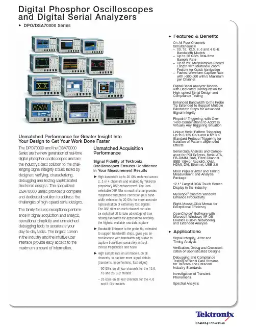
Features & BenefitsOn All Four Channels Simultaneously–20, 16, 12.5, 8, 6 and 4 GHzBandwidth Models–Up to 50 GS/s Real-time Sample Rate–Up to 200 Megasamples Record Length with MultiView Zoom ™Feature for Quick Navigation –Fastest Waveform Capture Rate with >300,000 wfm/s Maximum per Channel Digital Serial Analyzer Models with Dedicated Configuration for High-speed Serial Design and Compliance TestingEnhanced Bandwidth to the Probe Tip Extended to Support Multiple Bandwidth Steps for Advanced Signal IntegrityPinpoint ®Triggering, with Over 1400 Combinations to Address Virtually Any Triggering SituationUnique Serial Pattern Triggering Up to 3.125 Gb/s and 8 b/10 b Standard Protocol Triggering for Isolation of Pattern-dependent EffectsSerial Data Analysis and Compli-ance for PCI Express, Serial ATA,FB-DIMM, SAS, Fibre Channel,IEEE 1394b, RapidIO, XAUI,HDMI, DVI, Ethernet, USB 2.0 Most Popular Jitter and Timing Measurement and Analysis Package12.1" Largest XGA Touch Screen Display in the Industry MyScope ®Custom Windows Enhance Productivity Right-Mouse-Click Menus for Exceptional Efficiency OpenChoice ®Software with Microsoft Windows XP OS Enables Built-in Networking and Extended AnalysisApplicationsSignal Integrity, Jitter and Timing AnalysisVerification, Debug and Characteri-zation of Sophisticated Designs Debugging and Compliance Testing of Serial Data Streams for Telecom and Datacom Industry Standards Investigation of Transient Phenomena Spectral AnalysisDigital Phosphor Oscilloscopes and Digital Serial AnalyzersDPO/DSA70000 SeriesUnmatched Performance for Greater Insight Into Your Design to Get Your Work Done Faster The DPO70000 and the DSA70000Series are the new generation of real-timedigital phosphor oscilloscopes and arethe industry’s best solution to the chal-lenging signal integrity issues faced by designers verifying, characterizing,debugging and testing sophisticated electronic designs. The specialized DSA70000 Series provides a complete and dedicated solution to address the challenges of high-speed serial designs. The family features exceptional perform-ance in signal acquisition and analysis,operational simplicity and unmatched debugging tools to accelerate your day-to-day tasks. The largest screen in the industry and the intuitive user interface provide easy access to the maximum amount of information.Unmatched AcquisitionPerformance Signal Fidelity of TektronixOscilloscopes Ensures Confidence in Your Measurement ResultsHigh bandwidth up to 20GHz matched across 2,3 or 4 channels and enabled by Tektronix proprietary DSP enhancement.The user-selectable DSP filter on each channel provides magnitude and phase correction plus band-width extension to 20GHz for more accurate representation of extremely fast signals.The DSP filter on each channel can also be switched off to take advantage of true analog bandwidth for applications needing the highest available raw data capture Bandwidth Enhance to the probe tip,extended to support bandwidth steps,gives you an oscilloscope with bandwidth adjustable to capture transitions accurately without excess frequencies and noise High sample rate on all models,on all channels,to capture more signal details (transients,imperfections,fast edges) – 50 GS/s on all four channels for the 12.5,16 and 20 GHz models– 25 GS/s on all four channels for the 4,6and 8 GHz modelsDigital Phosphor Oscilloscopes and Digital Serial AnalyzersDPO/DSA70000 Seriesto provide very high trigger sensitivity with Zoom in on four areas of interest simultane-ously to compare them.Tektronix family of Z-Active probes.Maximize the probability of capturing elusiveglitches and other infrequent events withFastAcq acquisition mode.Isolate glitches down to 100ps wide.Isolate only the valid glitches.Digital Phosphor Oscilloscopes and Digital Serial AnalyzersDPO/DSA70000 SeriesOscilloscope • /oscilloscopes 3Protocol and Serial Pattern TriggeringSerial pattern triggering to debug pattern-dependent issues.How does a 12.1" display compare to the display size of other oscilloscopes?Drag-and-drop menu items of interest to create the MyScope ®control window.Digital Phosphor Oscilloscopes and Digital Serial Analyzers DPO/DSA70000 SeriesBasic spectral UI control window.Capture data into Microsoft Excel using theunique Excel toolbar,and create customreports using the Word toolbar.Oscilloscope • /oscilloscopes 5Digital Phosphor Oscilloscopes and Digital Serial AnalyzersDPO/DSA70000 SeriesCommunications Mask T esting – This Serial Data Compliance and Analysis –Optional HDMI Compliance T esting Jitter and Timing Measurement.Test eye diagram in equivalent time against the standard mask.RT-Eye ®version 2.0 – PCI Express Rev1.1Compliance test.HDMI compliance testing.UWB WiMedia analysis and measurements.Digital Phosphor Oscilloscopes and Digital Serial AnalyzersDPO/DSA70000 SeriesOptional Power Measurement and DSA70000 Series The DSA70000 Series Analyzers provideEthernet compliance B compliance testing.Power measurements and analysis.Oscilloscope • /oscilloscopes 7Digital Phosphor Oscilloscopes and Digital Serial AnalyzersDPO/DSA70000 SeriesOscilloscope • /oscilloscopes 9Digital Phosphor Oscilloscopes and Digital Serial AnalyzersDPO/DSA70000 SeriesDigital Phosphor Oscilloscopes and Digital Serial AnalyzersDPO/DSA70000 SeriesOscilloscope • /oscilloscopes 8Spread Spectrum Clock profiling.XAUI compliance testing.FB-DIMM compliance testing.Protocol Trigger.Protocol Decode.User-definable FIR filters for advanced analysis.11534961051107829Digital Phosphor Oscilloscopes and Digital Serial AnalyzersDPO/DSA70000 SeriesCharacteristicsDC Gain Accuracy±2% (of reading)Hardware Bandwidth Limits Requires TCA-1MEG AdapterInput Coupling DC (50 Ω),GNDInput Impedance 50Ω±1.5%,1 MΩwith TCA-1MEG adapterInput Sensitivity18GHz and below 10 mV/div to 1 V/div (100 mV to 10 V full scale)20GHz20 to 99.5 mV/div and 200 mV/div to 1 V/divVertical Resolution8bit (11 bit with averaging)Max Input Voltage,1MΩNot ApplicableMax Input Voltage,50Ω< 5.5VRMSfor ≥1 V full scale; also determined by TekConnect accessory Position Range±5 divOffset Range10 mV/div:±450 mV20 mV/div:±400 mV50 mV/div:±250 mV100 mV/div:±4.5 V200 mV/div:±4.0 V500 mV/div:±2.5 V1.0 V/div:0Offset Accuracy10 mV/div - 99.5mV/div:±(0.35% (offset value-position) + 1.5 mV + 1% of full scale)100 mV/div - 1V/div :±(0.35% (offset value-position) + 15 mV + 1% of full scale) Delay between any two channels (typical)≤100 ps for any two channels with equal V/div and coupling settings≤50 ps with BW enhance enabled (BW+)Channel-to-channel Isolation (Any Two ≥150:1 (for input frequency 0 to 5 GHz)Channels at Equal Vertical Scale Settings)≥80:1 (for input frequency >5 GHz to 12 GHz)≥40:1 (for input frequency >12 GHz to 15 GHz)≥25:1 (for input frequency >15 GHz)Oscilloscope • /oscilloscopes 11Digital Phosphor Oscilloscopes and Digital Serial AnalyzersDPO/DSA70000 SeriesTime Base Delay –5.0ks to 1.0ks Time Range Channel-to-Channel Range ±75 nsTrigger Jitter (RMS) 1 ps RMS (typical)Jitter Noise Floor <450 fs RMS (for record duration <10 µs)(typical )(With BW+bandwidth enhance enabled)Time Base Accuracy±1.5 ppm initial accuracy,aging <1 ppm per yearDPO/DSA Models70404/70604/7080471254/71604/72004Maximum Record Length per Channel With Standard Configuration 10 M on all four channels (DPO70000Series only)20 M on all four channels (DSA70000Series only) With Record Length Opt.2XL 20 M on all four channels (DPO70000Series only)With Record Length Opt.5XL 50 M on all four channelsDigital Phosphor Oscilloscopes and Digital Serial AnalyzersDPO/DSA70000 SeriesFastAcq Acquisition Mode FastAcq optimizes the instrument for analysis of dynamic signalsand capture of infrequent eventsMaximum FastAcq Waveform Capture Rate>300,000 wfm/s on all 4 channels simultaneouslyWaveform Database Accumulate waveform database providing three-dimensional arrayof amplitude,time and countsSample Acquire sampled valuesPeak Detect Captures narrow glitches at all real-time sampling rates:1 ns at ≤125MS/s; 1/sample rate at ≥250MS/sAveraging From 2 to 10,000 waveforms included in averageEnvelope From 1 to 2x10⁹waveforms included in min-max envelopeHi-Res Real-time boxcar averaging reduces random noise and increases resolutionFastFrame™Acquisition Acquisition memory divided into segments; maximum trigger rate >310,000 waveformsper second.Time of arrival recorded with each eventRoll Mode Up to 10MS/s with a maximum record length of 40MOscilloscope • /oscilloscopes 13Digital Phosphor Oscilloscopes and Digital Serial AnalyzersDPO/DSA70000 SeriesDPO ModelsDSA Models70404/70604/70804/71254/71604/7200470404/70604/70804/71254/71604/72004Sensitivity Internal DC Coupled4% of full scale from DC to 50 MHz10% of full scale at 4 GHz 20% of full scale at 8GHz 40% of full scale at 11 GHzExternal (Auxiliary Input) 50 Ω250mV from DC to 50 MHz,increasing to 350 mV at 1.0 GHzTrigger CharacteristicsA Event and DelayedB Event Trigger Types Edge,Glitch,Runt,Width,Transition Time,Timeout,Pattern,State,Setup/Hold,Window – all exceptEdge,Pattern and State can be Logic State qualified by up to two channelsMain Trigger Modes Auto,Normal and SingleTrigger SequencesMain,Delayed by Time,Delayed by Events,Reset by Time,Reset by State,Reset by Transition.All sequences Support for AMI,HDB3,BnZS,CMI,MLT3 and NRZ encoded communications signals.Select among Up to 64-bit serial word recognizer,bits specified in binary (high,low,don’t care) or hex format.Trigger on NRZ-encoded data up to 1.25GBaudClock Recovery Phase Locked Loop Bandwidth Fixed at FBaud/1600 Frequency Range 1.5 MBaud to 3.125 GBaudClock Recovery Jitter (RMS)<0.25% bit period + 2 ps RMS for PRBS data patterns<0.25% bit period + 1.5 ps RMS for repeating “0011”data patternTracking/Acquisition Range±2% of requested baud Minimum Signal Amplitude needed for Clock Recovery 1 div pk-pk up to 1.25 Gbaud 1.5 div pk-pk above 1.25 GbaudTrigger Level Range Internal ±120% of full scale from center of screenAUX Trigger TekConnect ®interface:±5 VLineFixed at 0 VTrigger CouplingDC,AC (attenuates <100 Hz),HF Rej (attenuates >20 kHz),LF Rej (attenuates <200 kHz),Noise Reject (reduces sensitivity)Trigger Holdoff Range250 ns min to 12 s maxDigital Phosphor Oscilloscopes and Digital Serial Analyzers DPO/DSA70000 SeriesOscilloscope • /oscilloscopes 15Digital Phosphor Oscilloscopes and Digital Serial AnalyzersDPO/DSA70000 SeriesAll rights reserved. The Tektronix Customer Service AdvantageEnsure the optimal performance of your T ektronix products andmaximize the lifetime value of your T ektronix investment.。


MSCSM120AM16CT1AGDatasheet Phase Leg MOSFET SiC Power ModuleJanuary20201Revision History (1)Revision1.0 (1)Product Overview (2)2.1Features (3)2.2Benefits (3)2.3Applications (3)Electrical Specifications (4)3.1SiC MOSFET Characteristics(Per MOSFET) (4)3.2SiC Schottky Diode Ratings Characteristics(Per SiC Diode) (6)3.3Thermal Package Characteristics (6)3.4Typical SiC MOSFET Performance Curves (8)3.5Typical SiC Diode Performance Curves (11)Package Specifications (12)Table1•Absolute Maximum Ratings (4)Table2•Electrical Characteristics (4)Table3•Dynamic Characteristics (5)Table4•Body Diode Ratings and Characteristics (5)Table5•SiC Schottky Diode Ratings and Characteristics (6)Table6•Package Characteristics (6)Table7•Temperature Sensor NTC1 (7)Figure1•MSCSM120AM16CT1AG Electrical Schematic (2)Figure2•MSCSM120AM16CT1AG Pinout Location (2)Figure3•Maximum Thermal Impedance (8)Figure4•Output Characteristics,TJ=25°C (8)Figure5•Output Characteristics,TJ=175°C (8)Figure6•Normalized RDS(on)vs.Temperature (8)Figure7•Transfer Characteristics (8)Figure8•Switching Energy vs.Rg (9)Figure9•Switching Energy vs.Current (9)Figure10•Capacitance vs.Drain Source Voltage (9)Figure11•Gate Charge vs.Gate Source Voltage (9)Figure12•Body Diode Characteristics,TJ=25°C (9)Figure13•3rd Quadrant Characteristics,TJ=25°C (9)Figure14•Body Diode Characteristics,TJ=175°C (10)Figure15•3rd Quadrant Characteristics,TJ=175°C (10)Figure16•Operating Frequency vs.Drain Current (10)Figure17•Maximum Thermal Impedance (11)Figure18•Forward Characteristics (11)Figure19•Capacitance vs.Reverse Voltage (11)Figure20•Package Outline (12)1Revision HistoryThe revision history describes the changes that were implemented in the document.The changes are listed by revision,starting with the most current publication.1.1Revision 1.0Revision 1.0is the first publication of this document,published in January 2020.Revision HistoryThe MSCSM120AM16CT1AG is a phase leg1200V/173A Silicon Carbide power module.Figure1•MSCSM120AM16CT1AG Electrical SchematicFigure2•MSCSM120AM16CT1AG Pinout LocationAll ratings at T J=25°C unless otherwise specified.Caution:These devices are sensitive to electrostatic discharge.Proper handling procedures should befollowed.2.1FeaturesThe following are key features of the MSCSM120AM16CT1AG device:•SiC Power MOSFET◦Low RDS(on)◦High temperature performance•Silicon carbide(SiC)Schottky diode◦Zero reverse recovery◦Zero forward recovery◦Temperature-independent switching behavior◦Positive temperature coefficient on VF•Very low stray inductance•Internal thermistor for temperature monitoring•Aluminum nitride(AlN)substrate for improved thermal performance 2.2BenefitsThe following are benefits of the MSCSM120AM16CT1AG device:•High power and high efficiency converters and inverters•Outstanding performance at high frequency operation•Direct mounting to heatsink(isolated package)•Low junction-to-case thermal resistance•Solderable terminals both for power and signal for easy PCB mounting•Low profile•RoHS Compliant2.3ApplicationsThe MSCSM120AM16CT1AG device is designed for the following applications:•Welding converters•Switched Mode Power Supplies•Uninterruptible Power Supplies•EV motor and traction drive3Electrical SpecificationsThis section shows the electrical specifications of the MSCSM120AM16CT1AG device.3.1SiC MOSFET Characteristics (Per MOSFET)This section describes the electrical characteristics of the MSCSM120AM16CT1AG device.Table 1•Absolute Maximum RatingsUnit Maximum Ratings ParameterSymbol V 1200Drain-source voltage V DSS A1731T C =25°C Continuous drain currentI D1381T C =80°C350Pulsed drain current I DM V –10/25Gate-source voltage V GS mΩ16Drain-source ON resistance R DSon W 745T C =25°CPower dissipationP DNote:1.Specification of SiC MOSFET device but output current must be limited due to the size of power connectors.Table 2•Electrical CharacteristicsUnit Max Typ MinTest Conditions CharacteristicSymbol μA 20020V GS =0V;V DS =1200V Zero gate voltage drain current I DSS mΩ1612.5T J =25°C V GS =20V I D =80ADrain–source on resistanceR DSon20T J =175°CV 2.81.8V GS =V DS ,I D =2mA Gate threshold voltage V GS(th)nA200V GS =20V,V DS =0VGate–source leakage currentI GSSTable 3•Dynamic CharacteristicsUnit MaxTyp MinTest Conditions Characteristic Symbol pF6040V GS =0V V DS =1000V f =1MHzInput capacitance C iss 540Output capacitance C oss 50Reverse transfer capacitance C rss nC464V GS =–5/20V V Bus =800V Total gate charge Q g 82Gate–source charge Q gs I D =80A 100Gate–drain charge Q gd ns 30V GS =–5/20V V Bus =600V Turn-on delay time T d(on)30Rise time T r I D =100A50Turn-off delay time T d(off)R Gon =4Ω;R Goff =2.4Ω25Fall time T f mJ 1.98T J =150°CInductive Switching V GS =–5/20V Turn on energy E on mJ1.3T J =150°CTurn off energyE offV Bus =600V I D =100A R Gon =4ΩR Goff =2.4ΩΩ2.94Internal gate resistanceR Gint °C/W0.2Junction-to-case thermal resistanceR thJCTable 4•Body Diode Ratings and CharacteristicsUnit MaxTyp MinTest Conditions Characteristic Symbol V4V GS =0V;I SD =80A Diode forward voltageV SD4.2V GS =–5V;I SD =80Ans 90I SD =80A;V GS =–5V;V R =800V;diF/dt =2000A/μsReverse recovery time t rr nC 1100Reverse recovery charge Q rr A27Reverse recovery currentI rr3.2SiC Schottky Diode Ratings Characteristics (Per SiC Diode)This section shows the SiC Schottky diode ratings and characteristics of the device.Table 5•SiC Schottky Diode Ratings and CharacteristicsUnit Max TypMinTest ConditionsCharacteristicSymbol V 1200Peak repetitive reverse voltage V RRM μA40020T J =25°C V R =1200VReverse leakage currentI RRM300T J =175°CA 60T C =100°C Forward current I F V1.81.5T J =25°C I F =60ADiode forward voltageV F2.1T J =175°CnC 260V R =600VTotal capacitive charge Q C pF282f =1MHz,V R =400V Total capacitanceC210f =1MHz,V R =800V°C/W 0.477Junction-to-case thermal resistanceR thJC3.3Thermal Package CharacteristicsThis section shows the thermal and package characteristics of the device.Table 6•Package CharacteristicsUnit MaxMin CharacteristicSymbol V 4000RMS isolation voltage,any terminal to case t =1min,50/60Hz V ISOL °C 175–40Operating junction temperature rangeT J °C T J max –25–40Recommended junction temperature under switching conditions T JOP °C 125–40Storage temperature range T STG °C 125–40Operating case temperature T C N.m 32M4To heatsinkMounting torque Torque g80Package weightWtTable 7•Temperature Sensor NTC 1Unit MaxTyp MinCharacteristic Symbol kΩ50Resistance at 25°CR 25%5ΔR 25/R 25K 3952T 25=298.15KB 25/85%4T C =100°CΔB/BNote:1. See application note APT0406 on .3.4Typical SiC MOSFET Performance CurvesThis section shows the typical performance curves of the MSCSM120AM016CT1AG SiC MOSFET.Figure3•Maximum Thermal ImpedanceFigure4•Output Characteristics,T J=25°CFigure6•Normalized RDS(on)vs.TemperatureFigure8•Switching Energy vs.Rg Figure9•Switching Energy vs.CurrentFigure10•Capacitance vs.Drain Source VoltageFigure12•Body Diode Characteristics,T J=25°C°CFigure16•Operating Frequency vs.Drain Current3.5Typical SiC Diode Performance CurvesThis section shows the typical performance curves of the MSCSM120AM16CT1AG SiC diode.Figure17•Maximum Thermal ImpedanceFigure18•Forward CharacteristicsThis section shows the package outline of the MSCSM120AM16CT1AG device.All dimensions are inmillimeters.Figure20•Package OutlineMicrosemi's product warranty is set forth in Microsemi's Sales Order Terms and rmation contained in this publication is provided for the sole purpose of designing with and using Microsemi rmation regarding device applications and the like is provided only for your convenience and may be superseded by updates.Buyer shall not rely on any data and performance specifications or parameters provided by Microsemi.It is your responsibility to ensure that your application meets with your specifications.THIS INFORMATION IS PROVIDED "AS IS."MICROSEMI MAKES NO REPRESENTATIONS OR WARRANTIES OF ANY KIND WHETHER EXPRESS OR IMPLIED,WRITTEN OR ORAL,STATUTORY OR OTHERWISE,RELATED TO THE INFORMATION,INCLUDING BUT NOT LIMITED TO ITS CONDITION,QUALITY ,PERFORMANCE,NON-INFRINGEMENT,MERCHANTABILITY OR FITNESS FOR A PARTICULAR PURPOSE.IN NO EVENT WILL MICROSEMI BE LIABLE FOR ANY INDIRECT,SPECIAL,PUNITIVE,INCIDENTAL OR CONSEQUENTIAL LOSS,DAMAGE,COST OR EXPENSE WHATSOEVER RELATED TO THIS INFORMATION OR ITS USE,HOWEVER CAUSED,EVEN IF MICROSEMI HAS BEEN ADVISED OF THE POSSIBILITY OR THE DAMAGES ARE FORESEEABLE.TO THE FULLEST EXTENT ALLOWED BY LAW,MICROSEMI’S TOTAL LIABILITY ON ALL CLAIMS IN RELATED TO THIS INFORMATION OR ITS USE WILL NOT EXCEED THE AMOUNT OF FEES,IF ANY ,YOU PAID DIRECTLY TO MICROSEMI FOR THIS e of Microsemi devices in life support,mission-critical equipment or applications,and/or safety applications is entirely at the buyer’s risk,and the buyer agrees to defend and indemnify Microsemi from any and all damages,claims,suits,or expenses resulting from such use.No licenses are conveyed,implicitly or otherwise,under any Microsemi intellectual property rights unless otherwisestated.Microsemi2355W.Chandler Blvd.Chandler,AZ 85224USAWithin the USA:+1(480)792-7200Fax:+1(480)792-7277 ©2020Microsemi and its corporate affiliates.All rights reserved.Microsemi and the Microsemi logo are trademarks of Microsemi Corporation and its corporate affiliates.All other trademarks and service marks are the property of their respective owners.Microsemi Corporation,a subsidiary of Microchip Technology Inc.(Nasdaq:MCHP),and its corporate affiliates are leading providers of smart,connected and secure embedded control solutions.Their easy-to-use development tools and comprehensive product portfolio enable customers to create optimal designs which reduce risk while lowering total system cost and time to market.These solutions serve more than 120,000customers across the industrial,automotive,consumer,aerospace and defense,communications and computing markets.Headquartered in Chandler,Arizona,the company offers outstanding technical support along with dependable delivery and quality.Learn more at .MSCC-0344-DS-01054-1.0-0120Legal。

DescriptionTLE 5203 is an integrated power bridge with DMOS output stages for driving DC motors.This motor bridge is optimized for driving DC motors in reversible operation. The internal protective circuitry in particular ensures that no crossover currents can occur.Because the free-wheeling diodes are integrated, the external circuitry that is necessary is reduced to the capacitors on the supply voltage.The control inputs have TTL/CMOS-compatible levels.1) SIEMENS Power Technology3-A DC Motor Driver Overview SPT IC 1)TLE 5203Figure1Pin Configuration (top view)Pin Definitions and FunctionsPin No.Symbol Function1Q1Output of channel 1; Short-circuit proof, free-wheelingdiodes integrated for inductive loads2EF Error flag; TTL/CMOS-compatible output for error detection(open drain)3I1Control input 1; TTL/CMOS-compatible4GND Ground; connected internally to cooling fin5I2Control input 2; TTL/CMOS-compatible6V S Supply voltage; wire with capacitor matching load7Q2Output of channel 2; Short-circuit proof, free-wheelingdiodes integrated for inductive loadsCircuit DescriptionInput CircuitThe control inputs consist of TTL/CMOS-compatible Schmitt triggers with hysteresis. Buffer amplifiers are driven by these stages and convert the logic signal into the necessary form for driving the power output stages.Output StagesThe output stages form a switched H-bridge. Protective circuits make the outputs short-circuit proof to ground and to the supply voltage throughout the operating range. Positive and negative voltage spikes, which occur when switching inductive loads, are clamped by integrated power diodes.Functional Truth TableE1E2Q1Q2CommentsL L H L Motor turns counterclockwiseL H L H Motor turns clockwiseH L L L Brake;both low side transistors turned-ONH H Z Z Open circuit detectionNotes for Output StageSymbol ValueL Low side transistor is turned-ONHigh side transistor is turned-OFFH High side transistor is turned-ONLow side transistor is turned-OFFZ High side transistor is turned-OFFLow side transistor is turned-OFFMonitoring FunctionsAn internal circuit ensures that all output transistors are turned-OFF if the supply voltage is below the operating range.A monitoring circuit for each output transistor detects whether the particular transistor is active and in this case prevents the corresponding source transistor (sink transistor) from conducting in sink operation (source operation). Therefore no crossover currents can occur. Pulse-width operation is possible up to a maximum switching frequency of 1kHz for any load.Depending on the load current higher frequencies are possible.Protective FunctionVarious errors like short-circuit to +V S, ground or across the load are detected. All faults result in turn-OFF of the output stages after a delay of 40µs and setting of the error flag EF to ground. Changing the inputs resets the error flag.Output Shorted to Ground DetectionIf a high side transistor is switched on and its output is shorted to ground, the output current is limited to typ 8 A. After a delay of 40 µs all outputs will be switched off and the error flag EF is set to ground.Output Shorted to + V S and Overload DetectionAn internal circuit detects if the current through the low side transistor is higher than 4A typ. In this case all outputs are turned off after 40 µs and the error flag EF is set to ground.At a junction temperature higher than 160°C the thermal shutdown turns off, all four output stages commonly and the error flag is set without a delay.Open Load DetectionThe output Q1 has a 10 kΩ pull-up resistor and the output Q2 has a 10 kΩ pull-down resistor. If E1 and E2 are high, all output power stages are turned-OFF. In case of no load between Q1 and Q2 the output voltage Q1 is V S and Q2 is ground. This state will be detected by two comparators and an error flag will be set after a delay time of 40 µs. Changing the inputs resets the error flip flop.DiagnosisInput Output Diagnosis EFE1E2Q1Q2Shortedto GND Shortedto V SOverload Open LoadL L H L Q1Q2X–L L H L H Q2Q1X–L H L L L–Q1,Q2––L H H Z Z–––X LFigure2Simplified Schematic for Open Load DetectionFigure3Block Diagram1)During overload condition currents higher than 4 A can dynamically occur, before the device shuts off, without any damaging the device.2)Depending on load higher frequencies are possible.Absolute Maximum Ratings T j = – 40 to 150 °C ParameterSymbolLimit Values Unit Remarksmin.max.VoltageSupply voltage Supply voltage Logic input voltageDiagnostics output voltage V S V S V I1, 2V EF– 0.3– 1– 0.3– 0.340–77V V V V–t < 500 ms; I S < 5 A V S = 0 – 40 V–CurrentFree-wheeling current Output current 1)I F I Q – 4– 444A A T j ≤ 150°C–Junction temperature Storage temperature T j T stg– 40– 50150150°C °C––Thermal Resistance Junction-case Junction-ambient R th jC R th jA––465K/W K/W ––Operating Range Supply voltage Logic input voltage Switching frequency 2)Junction temperatureV S V I1, 2f T j6– 0.3–– 402471150V V kHz °C––––Electrical CharacteristicsVS= 6 to 18 V; T j = – 40 to 150 °CParameter Symbol Limit Values Unit Test Conditionmin.typ.max.GeneralQuiescent current Turn-ON delay Turn-OFF delay Turn-ON timeTurn-OFF timeUndervoltage Undervoltage Iqtd1td2trtfVSVS––––––––10–10–5.54.510201020105.95.2mAµsµsµsµsVVIL= 0 AInput to outputInput to outputIQ= 2.5 A;cf diagramIQ= 2.5 A;cf diagramIC ONIC OFFLogic Control inputsH-input voltage L-input voltage VIHVIL2.8––––1.2VV––Hysteresis ofinput voltage∆V I0.40.8 1.2V–H-input current L-input current IIII–2–10––42µAµAVI= V IHVI= V ILDiagnosis outputDelay timeL-output voltage Leakage current tdVEFIRD20––40––600.410µsVµA–I = 3 mA–Error detectionSwitching threshold U Switching threshold L Overcurrent 1VEHVELIF12232.72.743.53.55VVAError lowError highError low1)Values for RDSON are for t > 100 µs after applying + V S .OutputsRDSONU RDSONU RDSONL RDSONLDiode forward voltage Diode forward voltage Pull up/pull down––––V FU V FL R––––––5––––––100.40.650.40.651.51.525ΩΩΩΩV V k ΩV S > 6 V; T j = 25 °C 1)V S > 6 V; T j = 150 °C 1)V S > 6 V; T j = 25 °C 1)V S > 6 V; T j = 150 °C 1)I F = 3 A I F = 3 A–Electrical Characteristics (cont’d)V S = 6 to 18 V; T j = – 40 to 150 °C ParameterSymbolLimit Values Unit Test Conditionmin.typ.max.Figure4Test CircuitFigure5Timing DiagramFigure6Application CircuitDiagramsR ON Resistance of Output Stageover TemperatureForward Current of UpperFree-Wheeling Diode versus VoltageOutput Voltage on Diagnostics Output versus CurrentForward Current of LowerFree-Wheeling Diode versus Voltage0˚C 255075100150j0.2F 0.61 1.4VAED013040.201234= 25 ˚C= 150 ˚CA F0.61 1.4V T j T jOvercurrent Threshold versus Temperature Input Threshold versus Temperature Quiescent Currentversus Temperature Switching Threshold V EL, EH versus TemperatureFigure7Timing Diagram for Output Shorted to GroundFigure8Timing Diagram for Output Shorted to V SFigure9Timing Diagram for OvercurrentFigure10Timing Diagram for Open LoadPackage OutlinesSorts of PackingPackage outlines for tubes, trays etc. are contained in ourData Book “Package Information”.Dimensions in mmSorts of PackingPackage outlines for tubes, trays etc. are contained in ourData Book “Package Information”.Dimensions in mm SMD = Surface Mounted Device。
电力电子技术术语Absorber Circuit 吸收电路AC/ACFrequency Converter 交交变频电路AC power control 交流电力控制AC Power Controller 交流调功电路AC Power Electronic Switch 交流电力电子开关AC Voltage Controller 交流调压电路Asynchronous Modulation 异步调制Baker Clamping Circuit 贝克箝位电路Bi-directional Triode Thyristor 双向晶闸管Bipolar Junction Transistor-- BJT 双极结型晶体管Boost—Buck Chopper 升降压斩波电路Boost Chopper 升压斩波电路Boost Converter 升压变换器Bridge Reversible Chopper 桥式可逆斩波电路Buck Chopper 降压斩波电路Buck Converter 降压变换器Commutation 换流Conduction Angle 导通角Constant Voltage Constant Frequency--CVCF恒压恒频Continuous Conduction—-CCM (电流)连续模式Control Circuit控制电路CUK Circuit CUK 斩波电路Current Reversible Chopper 电流可逆斩波电路Current Source Type Inverter-—CSTI 电流(源)型逆变电路Cycloconvertor 周波变流器DC—AC—DC Converter 直交直电路DC Chopping 直流斩波DC Chopping Circuit直流斩波电路DC-DC Converter 直流-直流变换器Device Commutation 器件换流Direct Current Control 直接电流控制Discontinuous Conduction mode (电流)断续模式Displacement Factor 位移因数Distortion Power 畸变功率Double End Converter 双端电路Driving Circuit 驱动电路Electrical Isolation 电气隔离Fast Acting Fuse 快速熔断器Fast Recovery Diode 快恢复二极管Fast Recovery Epitaxial Diodes 快恢复外延二极管Fast Switching Thyristor 快速晶闸管Field Controlled Thyristor 场控晶闸管Flyback Converter 反激电流Forced Commutation 强迫换流Forward Converter 正激电路Frequency Converter 变频器Full Bridge Converter 全桥电路Full Bridge Rectifier 全桥整流电路Full Wave Rectifier 全波整流电路Fundamental Factor 基波因数Gate Turn—Off Thyristor-—GTO可关断晶闸管General Purpose Diode 普通二极管Giant Transistor-—GTR 电力晶体管Half Bridge Converter 半桥电路Hard Switching 硬开关High Voltage IC 高压集成电路Hysteresis Comparison 带环比较方式Indirect Current Control 间接电流控制Indirect DC-DC Converter 直接电流变换电路Insulated-Gate Bipolar Transistor--IGBT 绝缘栅双极晶体管Intelligent Power Module-—IPM 智能功率模块Integrated Gate—Commutated Thyristor—-IGCT集成门极换流晶闸管Inversion 逆变Latching Effect 擎住效应Leakage Inductance 漏感Light Triggered Thyristo-——LTT 光控晶闸管Line Commutation 电网换流Load Commutation 负载换流Loop Current 环流元件设备三绕组变压器:three—column transformer ThrClnTrans 双绕组变压器:double-column transformer DblClmnTrans 电容器:Capacitor并联电容器:shunt capacitor电抗器:Reactor母线:Busbar输电线:TransmissionLine发电厂:power plant断路器:Breaker刀闸(隔离开关):Isolator分接头:tap电动机:motor状态参数有功:active power无功:reactive power电流:current容量:capacity电压:voltage档位:tap position有功损耗:reactive loss无功损耗:active loss功率因数:power—factor功率:power功角:power-angle电压等级:voltage grade空载损耗:no-load loss铁损:iron loss铜损:copper loss空载电流:no-load current阻抗:impedance正序阻抗:positive sequence impedance 负序阻抗:negative sequence impedance 零序阻抗:zero sequence impedance电阻:resistor电抗:reactance电导:conductance电纳:susceptance无功负载:reactive load 或者QLoad有功负载: active load PLoad遥测:YC(telemetering)遥信:YX励磁电流(转子电流):magnetizing current 定子:stator功角:power—angle上限:upper limit下限:lower limit并列的:apposable高压: high voltage低压:low voltage中压:middle voltage电力系统power system发电机generator励磁excitation励磁器excitor电压voltage电流current母线bus变压器transformer升压变压器step—up transformer高压侧high side输电系统power transmission system输电线transmission line固定串联电容补偿fixed series capacitor compensation 稳定stability电压稳定voltage stability功角稳定angle stability暂态稳定transient stability电厂power plant能量输送power transfer交流AC装机容量installed capacity电网power system落点drop point开关站switch station双回同杆并架double-circuit lines on the same tower 变电站transformer substation补偿度degree of compensation高抗high voltage shunt reactor无功补偿reactive power compensation故障fault调节regulation裕度magin三相故障three phase fault故障切除时间fault clearing time极限切除时间critical clearing time切机generator triping高顶值high limited value强行励磁reinforced excitation线路补偿器LDC(line drop compensation)机端generator terminal静态static (state)动态dynamic (state)单机无穷大系统one machine - infinity bus system 机端电压控制AVR电抗reactance电阻resistance功角power angle有功(功率)active power无功(功率) reactive power功率因数power factor无功电流reactive current下降特性droop characteristics斜率slope额定rating变比ratio参考值reference value电压互感器PT分接头tap下降率droop rate仿真分析simulation analysis传递函数transfer function框图block diagram受端receive—side裕度margin同步synchronization失去同步loss of synchronization 阻尼damping摇摆swing保护断路器circuit breaker电阻:resistance电抗:reactance阻抗:impedance电导:conductance电纳:susceptance导纳:admittance电感:inductance电容:capacitance一般术语电力电子变流器的型式(表1—2)电力电子开关和交流电力电子控制器电力电子设备的基本元件电力电子设备的电路和电路单元电力电子设备的运行电力电子设备的性能电力电子变流器的特性曲线稳定电源。
Eaton 198575Eaton Moeller® series Rapid Link - Speed controller, 5.6 A, 2.2 kW, Sensor input 4, AS-Interface®, S-7.4 for 31 modules, HAN Q5, with manual override switch, with braking resistanceGeneral specificationsEaton Moeller® series Rapid Link Speed controller1985754015081964505157 mm 270 mm 220 mm 3.59 kg UL 61800-5-1 IEC/EN 61800-5-1 CE UL approval RoHSProduct NameCatalog NumberEANProduct Length/Depth Product Height Product Width Product Weight Certifications Catalog Notes 3 fixed speeds and 1 potentiometer speedcan be switched over from U/f to (vector) speed control Connection of supply voltage via adapter cable on round or flexible busbar junction Diagnostics and reset on device and via AS-Interface480 VIs the panel builder's responsibility. The specifications for the switchgear must be observed.400 V AC, 3-phase480 V AC, 3-phaseMeets the product standard's requirements.2.2 kW500 VMeets the product standard's requirements.-40 °C380 VInternal DC linkManual override switchBreaking resistanceKey switch position HANDPTC thermistor monitoringControl unitSelector switch (Positions: REV - OFF - FWD)Key switch position AUTOBraking resistancePC connectionKey switch position OFF/RESETThermo-click with safe isolationIGBT inverterTwo sensor inputs through M12 sockets (max. 150 mA) for quick stop and interlocked manual operation0 Hz Rapid Link 5 - brochureDA-SW-USB Driver DX-COM-STICK3-KITDA-SW-USB Driver PC Cable DX-CBL-PC-1M5DA-SW-Driver DX-CBL-PC-3M0DA-SW-drivesConnect - installation helpDA-SW-drivesConnectDA-SW-drivesConnect - InstallationshilfeMaterial handling applications - airports, warehouses and intra-logisticseaton-bus-adapter-rapidlink-speed-controller-dimensions-002.eps eaton-bus-adapter-rapidlink-speed-controller-dimensions-003.eps eaton-bus-adapter-rapidlink-speed-controller-dimensions-004.eps eaton-bus-adapter-rapidlink-speed-controller-dimensions-005.epsETN.RASP5-5400A31-512R100S1.edzIL034085ZUramo5_v20.dwgrasp5_v20.stpGeneration change from RA-MO to RAMO 4.0Generation change RAMO4 to RAMO5Generation change from RA-SP to RASP 4.0Generation Change RA-SP to RASP5Configuration to Rockwell PLC for Rapid LinkGeneration Change RASP4 to RASP5DA-DC-00003964.pdfDA-DC-00004184.pdfDA-DC-00004514.pdfDA-DC-00004508.pdfMains voltage - max10.11 Short-circuit ratingRated operational voltage10.4 Clearances and creepage distancesOutput at quadratic load at rated output voltage - max Output voltage - max10.2.3.1 Verification of thermal stability of enclosures Ambient storage temperature - minMains voltage - minFitted with:Output frequency - minStarting current - max BrochureDisegnieCAD modelIstruzioni di installazione mCAD modelNote per l'applicazione Report di certificazione200 %, IH, max. starting current (High Overload), For 2 seconds every 20 seconds, Power sectionRated conditional short-circuit current (Iq)10 kAAmbient operating temperature - max40 °CCommunication interfaceAS-InterfaceAssigned motor power at 115/120 V, 60 Hz, 1-phase3 HPOutput frequency - max500 HzSwitching frequency8 kHz, 4 - 32 kHz adjustable, fPWM, Power section, Main circuitFeaturesParameterization: FieldbusParameterization: KeypadDiagnostics and reset on device and via AS-Interface Parameterization: drivesConnect mobile (App) Parameterization: drivesConnectAmbient operating temperature - min-10 °CBraking current≤ 0.6 A (max. 6 A for 120 ms), Actuator for external motor brakeNumber of HW-interfaces (serial TTY)10.6 Incorporation of switching devices and componentsDoes not apply, since the entire switchgear needs to be evaluated.Nominal output current I2N5.6 A10.2.6 Mechanical impactDoes not apply, since the entire switchgear needs to be evaluated.10.3 Degree of protection of assembliesDoes not apply, since the entire switchgear needs to be evaluated.Product categorySpeed controllerRadio interference classC2, C3: depending on the motor cable length, the connected load, and ambient conditions. External radio interference suppression filters (optional) may be necessary.C1: for conducted emissions onlyHeat dissipation capacity Pdiss0 WRated control voltage (Uc)24 V DC (-15 %/+20 %, external via AS-Interface® plug)Assigned motor power at 460/480 V, 60 Hz, 3-phase3 HPNumber of HW-interfaces (RS-422)Mains current distortion120 %ProtocolAS-Interface profile cable: S-7.4 for 31 modulesASI10.9.2 Power-frequency electric strengthIs the panel builder's responsibility.Overvoltage categoryIIIDegree of protectionIP65NEMA 12Ambient storage temperature - max70 °CRated impulse withstand voltage (Uimp)2000 VConnectionPlug type: HAN Q5Overload currentAt 40 °CFor 60 s every 600 sFunctionsBrake chopper with braking resistance for dynamic braking 4-quadrant operation possible3 fixed speeds1 potentiometer speedOutput at linear load at rated output voltage - max2.2 kWMains voltage tolerance380 - 480 V (-10 %/+10 %, at 50/60 Hz)Leakage current at ground IPE - max3.5 mAConverter typeU converter10.2.2 Corrosion resistanceMeets the product standard's requirements.Supply frequency50/60 Hz10.2.4 Resistance to ultra-violet (UV) radiationMeets the product standard's requirements.10.2.7 InscriptionsMeets the product standard's requirements.Shock resistance15 g, Mechanical, According to IEC/EN 60068-2-27, 11 ms, Half-sinusoidal shock 11 ms, 1000 shocks per shaftApplication in domestic and commercial area permittedYesNumber of inputs (analog)Number of phases (output)310.12 Electromagnetic compatibilityIs the panel builder's responsibility. The specifications for the switchgear must be observed.10.2.5 LiftingDoes not apply, since the entire switchgear needs to be evaluated.Number of HW-interfaces (RS-485)1Number of HW-interfaces (industrial ethernet)Efficiency98 % (η)System configuration typeAC voltagePhase-earthed AC supply systems are not permitted.Center-point earthed star network (TN-S network)10.8 Connections for external conductorsIs the panel builder's responsibility.Switch-on threshold for the braking transistor765 VDCProtectionFinger and back-of-hand proof, Protection against direct contact (BGV A3, VBG4)Application in industrial area permittedYesClimatic proofing< 95 %, no condensationIn accordance with IEC/EN 5017810.9.3 Impulse withstand voltageIs the panel builder's responsibility.Overload current IL at 150% overload8.4 AInput current ILN at 150% overload5.3 ANumber of HW-interfaces (RS-232)Number of inputs (digital)4Current limitationAdjustable, motor, main circuit0.5 - 5.6 A, motor, main circuitCable lengthC1 ≤ 1 m, maximum motor cable lengthC2 ≤ 5 m, maximum motor cable lengthC3 ≤ 25 m, maximum motor cable length10.5 Protection against electric shockDoes not apply, since the entire switchgear needs to be evaluated.Mounting positionVerticalMains switch-on frequencyMaximum of one time every 60 seconds10.13 Mechanical functionThe device meets the requirements, provided the information in the instruction leaflet (IL) is observed.10.9.4 Testing of enclosures made of insulating materialIs the panel builder's responsibility.Heat dissipation per pole, current-dependent Pvid0 WElectromagnetic compatibility1st and 2nd environments (according to EN 61800-3)Resolution0.1 Hz (Frequency resolution, setpoint value)Assigned motor power at 460/480 V, 60 Hz3 HPRelative symmetric net voltage tolerance10 %Rated operational current (Ie)5.6 A at 150% overload (at an operating frequency of 8 kHz and an ambient air temperature of +40 °C)Number of outputs (analog)Rated operational power at 380/400 V, 50 Hz, 3-phase2.2 kWNumber of HW-interfaces (USB)Operating modePM and LSPM motorsSynchronous reluctance motorsSensorless vector control (SLV)U/f controlBLDC motorsRated frequency - min45 HzDelay time< 10 ms, Off-delay< 10 ms, On-delayNumber of outputs (digital)Power consumption58 W10.2.3.2 Verification of resistance of insulating materials to normal heatMeets the product standard's requirements.10.2.3.3 Resist. of insul. mat. to abnormal heat/fire by internal elect. effectsMeets the product standard's requirements.Number of HW-interfaces (other)1Rated frequency - max66 HzVibrationResistance: 57 Hz, Amplitude transition frequency on accelerationResistance: According to IEC/EN 60068-2-6Resistance: 10 - 150 Hz, Oscillation frequencyResistance: 6 Hz, Amplitude 0.15 mmShort-circuit protection (external output circuits)Type 1 coordination via the power bus' feeder unit, Main circuit10.7 Internal electrical circuits and connectionsIs the panel builder's responsibility.Braking torqueAdjustable to 100 % (I/Ie), DC - Main circuitRelative symmetric net frequency tolerance10 %10.10 Temperature riseThe panel builder is responsible for the temperature rise calculation. Eaton will provide heat dissipation data for the devices.Number of HW-interfaces (parallel)Assigned motor power at 230/240 V, 60 Hz, 1-phase3 HPInterfacesNumber of slave addresses: 31 (AS-Interface®)Max. total power consumption from AS-Interface® power supply unit (30 V): 190 mASpecification: S-7.4 (AS-Interface®)Number of phases (input)Eaton Corporation plc Eaton House30 Pembroke Road Dublin 4, Ireland © 2023 Eaton. Tutti i diritti riservati. Eaton is a registered trademark.All other trademarks areproperty of their respectiveowners./socialmedia336.6 W at 25% current and 0% speed 38.1 W at 25% current and 50% speed 42 W at 50% current and 0% speed 42.5 W at 50% current and 90% speed 44.2 W at 50% current and 50% speed 55.9 W at 100% current and 0% speed 58.3 W at 100% current and 90% speed 60.4 W at 100% current and 50% speed 0Above 1000 m with 1 % performance reduction per 100 m Max. 2000 mHeat dissipation at current/speed Number of interfaces (PROFINET)Altitude。
1 Power Electronic ConceptsPower electronics is a rapidly developing technology. Components are tting higher current and voltage ratings, the power losses decrease and the devices become more reliable. The devices are also very easy tocontrol with a mega scale power amplification. The prices are still going down pr. kVA and power converters are becoming attractive as a mean to improve the performance of a wind turbine. This chapter will discuss the standard power converter topologies from the simplest converters for starting up the turbine to advanced power converter topologies, where the whole power is flowing through the converter. Further, different park solutions using power electronics arealso discussed.1.1 Criteria for concept evaluationThe most common topologies are selected and discussed in respect to advantages and drawbacks. Very advanced power converters, where many extra devices are necessary in order to get a proper operation, are omitted.1.2 Power convertersMany different power converters can be used in wind turbine applications. In the case of using an induction generator, the power converter has to convert from a fixed voltage and frequency to a variable voltage and frequency. This may be implemented in many different ways, as it will be seen in the next section. Other generator types can demand other complex protection. However, the most used topology so far is a soft-starter, which is used during start up in order to limit the in-rush current and thereby reduce the disturbances to the grid.1.2.1 Soft starterThe soft starter is a power converter, which has been introduced to fixedspeed wind turbines to reduce the transient current during connection or disconnection of the generator to the grid. When the generator speed exceeds the synchronous speed, the soft-starter is connected. Using firing angle control of the thyristors in the soft starter the generator is smoothly connected to the grid over a predefined number of grid periods. An example of connection diagram for the softstarter with a generator is presented in Figure1.Figure 1. Connection diagram of soft starter with generators.The commutating devices are two thyristors for each phase. These are connected in anti-parallel. The relationship between the firing angle (﹤) and the resulting amplification of the soft starter is non-linear and depends additionally on the power factor of the connected element. In the case of a resistive load, may vary between 0 (full on) and 90 (full off) degrees, in the case of a purely inductive load between 90 (full on) and 180 (full off) degrees. For any power factor between 0 and 90 degrees, w ill be somewhere between the limits sketched in Figure 2.Figure 2. Control characteristic for a fully controlled soft starter.When the generator is completely connected to the grid a contactor (Kbyp) bypass the soft-starter in order to reduce the losses during normal operation. The soft-starter is very cheap and it is a standard converter in many wind turbines.1.2.2 Capacitor bankFor the power factor compensation of the reactive power in the generator, AC capacitor banks are used, as shown in Figure 3. The generators are normally compensated into whole power range. The switching of capacitors is done as a function of the average value of measured reactive power during a certain period.Figure 3. Capacitor bank configuration for power factor compensation ina wind turbine.The capacitor banks are usually mounted in the bottom of the tower or in thenacelle. In order to reduce the current at connection/disconnection of capacitors a coil (L) can be connected in series. The capacitors may be heavy loaded and damaged in the case of over-voltages to the grid and thereby they may increase the maintenance cost.1.2.3 Diode rectifierThe diode rectifier is the most common used topology in power electronic applications. For a three-phase system it consists of six diodes. It is shown in Figure 4.Figure 4. Diode rectifier for three-phase ac/dc conversionThe diode rectifier can only be used in one quadrant, it is simple and it is notpossible to control it. It could be used in some applications with a dc-bus.1.2.4 The back-to-back PWM-VSIThe back-to-back PWM-VSI is a bi-directional power converter consisting of two conventional PWM-VSI. The topology is shown in Figure 5.To achieve full control of the grid current, the DC-link voltage must be boosted to a level higher than the amplitude of the grid line-line voltage. The power flow of the grid side converter is controlled in orderto keep the DC-link voltage constant, while the control of the generator side is set to suit the magnetization demand and the reference speed. The control of the back-to-back PWM-VSI in the wind turbine application is described in several papers (Bogalecka, 1993), (Knowles-Spittle et al., 1998), (Pena et al., 1996), (Yifan & Longya, 1992), (Yifan & Longya, 1995).Figure 5. The back-to-back PWM-VSI converter topology.1.2.4.1 Advantages related to the use of the back-to-back PWM-VSIThe PWM-VSI is the most frequently used three-phase frequency converter. As a consequence of this, the knowledge available in the field is extensive and well established. The literature and the available documentation exceed that for any of the other converters considered in this survey. Furthermore, many manufacturers produce components especially designed for use in this type of converter (e.g., a transistor-pack comprising six bridge coupled transistors and anti paralleled diodes). Due to this, the component costs can be low compared to converters requiring components designed for a niche production.A technical advantage of the PWM-VSI is the capacitor decoupling between the grid inverter and the generator inverter. Besides affording some protection, this decoupling offers separate control of the two inverters, allowing compensation of asymmetry both on the generator side and on the grid side, independently.The inclusion of a boost inductance in the DC-link circuit increases the component count, but a positive effect is that the boost inductance reduces the demands on the performance of the grid side harmonic filter, and offers some protection of the converter against abnormal conditions on the grid.1.2.4.2 Disadvantages of applying the back-to-back PWM-VSIThis section highlights some of the reported disadvantages of the back-to-back PWM-VSI which justify the search for a more suitable alternative converter:In several papers concerning adjustable speed drives, the presence of the DC link capacitor is mentioned as a drawback, since it is heavy and bulky, it increases the costs and maybe of most importance, - it reduces the overall lifetime of the system. (Wen-Song & Ying-Yu, 1998); (Kim & Sul, 1993); (Siyoung Kim et al., 1998).Another important drawback of the back-to-back PWM-VSI is the switching losses. Every commutation in both the grid inverter and the generator inverter between the upper and lower DC-link branch is associated with a hard switching and a natural commutation. Since the back-to-back PWM-VSI consists of two inverters, the switching losses might be even more pronounced. The high switching speed to the grid may also require extra EMI-filters.To prevent high stresses on the generator insulation and to avoid bearing current problems (Salo & Tuusa, 1999), the voltage gradient may have to be limited by applying an output filter.1.2.5 Tandem converterThe tandem converter is quite a new topology and a few papers only have treated it up till now ((Marques & Verdelho, 1998); (Trzynadlowski et al., 1998a); (Trzynadlowski et al., 1998b)). However, the idea behind the converter is similar to those presented in ((Zhang et al., 1998b)), where the PWM-VSI is used as an active harmonic filter to compensate harmonic distortion. The topology of the tandem converter is shown inFigure 6.Figure 6. The tandem converter topology used in an induction generator wind turbine system.The tandem converter consists of a current source converter, CSC, in thefollowing designated the primary converter, and a back-to-back PWM-VSI, designated the secondary converter. Since the tandem converter consists of four controllable inverters, several degrees of freedom exist which enable sinusoidal input and sinusoidal output currents. However, in this context it is believed that the most advantageous control of the inverters is to control the primary converter to operate in square-wave current mode. Here, the switches in the CSC are turned on and off only once per fundamental period of the input- and output current respectively. In square wave current mode, the switches in the primary converter may either be GTO.s, or a series connection of an IGBT and a diode.Unlike the primary converter, the secondary converter has to operateat a high switching frequency, but the switched current is only a small fraction of the total load current. Figure 7 illustrates the current waveform for the primary converter, the secondary converter, is, and the total load current il.In order to achieve full control of the current to/from the back-to-back PWMVSI, the DC-link voltage is boosted to a level above the grid voltage. As mentioned, the control of the tandem converter is treated in only a few papers. However, the independent control of the CSC and the back-to-back PWM-VSI are both well established, (Mutschler & Meinhardt, 1998); (Nikolic & Jeftenic, 1998); (Salo & Tuusa, 1997); (Salo & Tuusa, 1999).Figure 7. Current waveform for the primary converter, ip, the secondary converter, is, and the total load current il.1.2.5.1Advantages in the use of the Tandem ConverterThe investigation of new converter topologies is commonly justifiedby thesearch for higher converter efficiency. Advantages of the tandem converter are the low switching frequency of the primary converter, and the low level of the switched current in the secondary converter. It is stated that the switching losses of a tandem inverter may be reduced by 70%, (Trzynadlowski et al., 1998a) in comparison with those of an equivalent VSI, and even though the conduction losses are higher for the tandem converter, the overall converter efficiency may be increased.Compared to the CSI, the voltage across the terminals of the tandem converter contains no voltage spikes since the DC-link capacitor of the secondary converter is always connected between each pair of input- and output lines (Trzynadlowski et al., 1998b).Concerning the dynamic properties, (Trzynadlowski et al., 1998a) states that the overall performance of the tandem converter is superior to both the CSC and the VSI. This is because current magnitude commands are handled by the voltage source converter, while phase-shift current commands are handled by the current source converter (Zhang et al., 1998b).Besides the main function, which is to compensate the current distortion introduced by the primary converter, the secondary converter may also act like an active resistor, providing damping of the primary inverter in light load conditions (Zhang et al., 1998b).1.2.5.2 Disadvantages of using the Tandem ConverterAn inherent obstacle to applying the tandem converter is the high number of components and sensors required. This increases the costs and complexity of both hardware and software. The complexity is justified by the redundancy of the system (Trzynadlowski et al., 1998a), however the system is only truly redundant if a reduction in power capability and performance is acceptable.Since the voltage across the generator terminals is set by the secondary inverter, the voltage stresses at the converter are high.Therefore the demands on the output filter are comparable to those when applying the back-to-back PWM-VSI.In the system shown in Figure 38, a problem for the tandem converter in comparison with the back-to-back PWM-VSI is the reduced generator voltage. By applying the CSI as the primary converter, only 0.866% of the grid voltage can be utilized. This means that the generator currents (and also the current through the switches) for the tandem converter must be higher in order to achieve the same power.1.2.6 Matrix converterIdeally, the matrix converter should be an all silicon solution with no passive components in the power circuit. The ideal conventional matrix converter topology is shown in Figure 8.Figure 8. The conventional matrix converter topology.The basic idea of the matrix converter is that a desired input current (to/from the supply), a desired output voltage and a desired output frequency may be obtained by properly connecting the output terminals of the converter to the input terminals of the converter. In order to protect the converter, the following two control rules must be complied with: Two (or three) switches in an output leg are never allowed to be on at the same time. All of the three output phases must be connected to an input phase at any instant of time. The actual combination of the switchesdepends on the modulation strategy.1.2.6.1 Advantages of using the Matrix ConverterThis section summarises some of the advantages of using the matrix converter in the control of an induction wind turbine generator. For a low output frequency of the converter the thermal stresses of the semiconductors in a conventional inverter are higher than those in a matrix converter. This arises from the fact that the semiconductors in a matrix converter are equally stressed, at least during every period of the grid voltage, while the period for the conventional inverter equals the output frequency. This reduces thethermal design problems for the matrix converter.Although the matrix converter includes six additional power switches compared to the back-to-back PWM-VSI, the absence of the DC-link capacitor may increase the efficiency and the lifetime for the converter (Schuster, 1998). Depending on the realization of the bi-directional switches, the switching losses of the matrix inverter may be less than those of the PWM-VSI, because the half of the switchings become natural commutations (soft switchings) (Wheeler & Grant, 1993).1.2.6.2 Disadvantages and problems of the matrix converterA disadvantage of the matrix converter is the intrinsic limitation of the output voltage. Without entering the over-modulation range, the maximum output voltage of the matrix converter is 0.866 times the input voltage. To achieve the same output power as the back-to-back PWM-VSI, the output current of the matrix converter has to be 1.15 times higher, giving rise to higher conducting losses in the converter (Wheeler & Grant, 1993).In many of the papers concerning the matrix converter, the unavailability of a true bi-directional switch is mentioned as one of the major obstacles for the propagation of the matrix converter. In the literature, three proposals for realizing a bi-directional switch exists. The diode embedded switch (Neft & Schauder, 1988) which acts like a truebi-directional switch, the common emitter switch and the common collector switch (Beasant et al., 1989).Since real switches do not have infinitesimal switching times (which is not desirable either) the commutation between two input phases constitutes a contradiction between the two basic control rules of the matrix converter. In the literature at least six different commutation strategies are reported, (Beasant et al., 1990); (Burany, 1989); (Jung & Gyu, 1991); (Hey et al., 1995); (Kwon et al., 1998); (Neft & Schauder, 1988). The most simple of the commutation strategies are those reported in (Beasant et al., 1990) and (Neft & Schauder, 1988), but neither of these strategies complies with the basic control rules.译文1 电力电子技术的内容电力电子技术是一门正在快速发展的技术,电力电子元器件有很高的额定电流和额定电压,它的功率减小元件变得更加可靠、耐用.这种元件还可以用来控制比它功率大很多倍的元件。
Bulletin HY11-3237-M1/UKElectronic for Proportional Directional Control ValvesInstallation Manual Series PWD 00A-400Parker Hannifin GmbH & Co. KG Hydraulic Controls Division Gutenbergstr. 3841564 Kaarst, Germany Tel.: +49-181 99 44 43 0Fax: +49-2131-513-230E-mail: infohcd@Copyright © 2005, Parker Hannifin GmbH & Co. KG2IA PWD00A UK.INDD 11.06Electronic for Proportional DC Valves Series PWD 00A-400Installation ManualParker Hannifin GmbH & Co. KG Hydraulic Controls DivisionNoteThis document and other information from Parker Hannifin GmbH & Co. KG, its subsidiaries, sales offices and authorized distributors provide product or system options for further investigation by users having technical expertise. Before you select or use any product or system it is important that you analyse all aspects of your application and review the information concerning the product or system in the current product catalogue. Due to the variety of operating conditions and applications for these products or systems, the user, through his own analysis and testing, is solely responsible for making the final selection of the products and systems and assuring that all performance and safety requirements of the application are met. The products are subject to change by Parker Hannifin GmbH & Co. KG at any time without notice.Electronic for Proportional DC Valves Series PWD 00A-400Installation Manual3Parker Hannifin GmbH & Co. KG Hydraulic Controls DivisionIA PWD00A UK.INDD 11.06Circuit DiagramNoteThe operating software ProPXD is available for download on /euro_hcd or may be ordered under code 5715543.Parker electronic modules PWD00A-400 for rail mounting are compact, easy to install and provide time-saving wiring by disconnectable terminals. The digital design of the circuit results in good accuracy and optimal adaption for proportional directional control valves by a comfortable interface program.Characteristics of the electronic control module The described electronic unit combines all neces-sary functions for the optimal operation of propor-tional directional control valves without position sensor (series D*FB, D*FW, WLL, RLL). The most important features are:• digital circuit design• four parameterizable preset recall channels • constant current control • differential input stage • status output• four quadrant ramp function • enable input for solenoid driver • status indicator• parametering by serial interface RS-232• connection by disconnectable terminals•compatible to the relevant European EMC standards•comfortable interface program4IA PWD00A UK.INDD 11.06Electronic for Proportional DC ValvesSeries PWD 00A-400Installation ManualParker Hannifin GmbH & Co. KG Hydraulic Controls DivisionTechnical dataElectronic module directional valvesDesign seriesModule type Amplifier,adjustable Min./Max.-limits ac-cel.-/decel.-ramp for each solenoid,4 internal programmable commandsVariable solenoid currentOrdering CodeGeneral ModelModule package for snap-on mounting on EN 50022 rail Package material Polycarbonate Inflammability class V2..V0 acc. UL 94Installation position Any Ambient temperature range [°C]-20...+60Protection class NEMA (IP20) acc. EN 60529Weight [g]160Electrical Duty ratio [%]100Supply voltage [VDC]18...30, ripple < 5% eff., surge free 1)Switch-on current typ.[A]22 for 0.2 mS Current consumption max.[A] 2.0Pre-fusing [A] 2.5 A medium lagCommand signal [V]+10...0...-10, ripple < 0.01 % eff., surge free, Ri = 150 kOhm Input signal resolution [%]0,025Differential input voltage max.[V]30 for terminals 5 und 6 against PE (terminal 8)Enable signal [V]0...5.0: Off / 8,5...30: On / Ri = 30 kOhm Channel recall signal [V]0...5.0: Off / 8,5...30: On / Ri = 30 kOhm Status signal [V]0...0.5: Off / Us: On / rated max. 15 mA Adjustment ranges Min Max Ramp Zero offset Current [%][%][ms][%][A]0...50 preset 0...10050...100 preset 0...1000...32500 preset 0...32500+75...-75preset +100...-1000.8/1.3/1.8/2.7/3.5preset 0/4/3/2/1Interface RS 232C, DSub 9p. male for null modem cable EMC EN 50081-2, EN 50082-2Connection Screw terminals 0.2...2.5 mm², disconnectableCable specification [AWG][AWG]16 overall braid shield for supply voltage and solenoids 20 overall braid shield for sensor and signal Cable length[m]501)If solenoids with a nominal voltage of 24V are connected, the supply voltage has to be raised to 29V .A00PWD400Electronic for Proportional DC Valves Series PWD 00A-400Installation Manual5Parker Hannifin GmbH & Co. KG Hydraulic Controls DivisionIA PWD00A UK.INDD 11.06Signal flow diagramCommandsAdditionally to the external analogue command input (Pin 5 and 6), the PWD00A-400-electronic includes four internal programmable command values S1 toInternal Ramps S4, which can be activated by the switching inputs (Pins 13, 14, 15, 16). S1 at pin 13 has the highest priority, S4 at pin 16 the lowest.6IA PWD00A UK.INDD 11.06Electronic for Proportional DC Valves Series PWD 00A-400Installation ManualParker Hannifin GmbH & Co. KGHydraulic Controls DivisionRamp-function / Min-Max-functionThe PWD00A-400-Electronic includes four internal programable ramps. Acceleration and/or decelera-tion are adjustable for each solenoid separately.Additionally a current step may be programmed for each solenoid (Min), and the current may be limited for each solenoid (Max).Nominal current adjustmentThe nominal current can be adjusted by one param-eter separately for each solenoid (Pin 9, 10, and 11, 12). The default nominal current is 800mA.ParameterizationAll parameters can be adjusted via a serial con-nection (RS232-null modem) by the computer-software.The computer-software shows the parameters in text-form. So they are easy to use.All parameters are saved in an EEPROM and become active directly after supply voltage is switched on.The connected valve may not operated before loading an appropriate parameter set from the PC into the module electronics.Example of parameter chartParameterRange Default value Unit FunctionP10...±100.00%Zero point adjustment P2---ReservedP30...100.0100.0%Max. current A-solenoid P40...100.0100.0%Max. current B-solenoidP50...100%Dither amplitude, 10% = 1.6% max. current P60...8000Hz Dither frequencyP70...100.00%Min. current A-solenoid P80...100.00%Min. current B-solenoid S1-100.0...+100.00%Internal command 1S2-100.0...+100.00%Internal command 2S3-100.0...+100.00%Internal command 3S4-100.0...+100.00%Internal command 4S50...325000ms Acceleration A-solenoid S60...325000ms Deceleration A-solenoid S70...325000ms Acceleration B-solenoid S80...325000ms Deceleration B-solenoidIA 0, 1, 2, 3, 4--Nom. current A-solenoid, 0=0.8A; 1=3.5A; 2=2.7A; 3=1.8A; 4=1.3A IB 0, 1, 2, 3, 4--Nom. current B-solenoid, 0=0.8A; 1=3.5A; 2=2.7A; 3=1.8A; 4=1.3A E250, 1-Operating threshold MIN, 0=1%, 1=0.1%Electronic for Proportional DC Valves Series PWD 00A-400Installation Manual7Parker Hannifin GmbH & Co. KG Hydraulic Controls DivisionIA PWD00A UK.INDD 11.06Connection ExamplesCertainly modifications and / or combinations of these examples are possible. The priority of the digital inputs over the analogue input has to be kept in mind!Standard ParamtersValve SolenoidNominal CurrentDitherI max A-side (IA)I max B-side (IB)Amplitude (P5)[%]Frequency (P6)[Hz]D1FW K 1.8A (3) 1.8A (3) 2.0100M 2.7A (2) 2.7A (2) 2.0100L 3.5A (1) 3.5A (1) 2.0100D1FB M 2.7A (2) 2.7A (2) 2.0100D3FW K 2.7A (2) 2.7A (2) 2.0100M 3.5A (1) 3.5A (1) 2.0100D3FB M 3.5A (1) 3.5A (1) 2.0130RLL NG06G09 2.7A (2) 2.7A (2) 2.0130WLL NG06G09 2.7A (2) 2.7A (2) 2.0110WLL NG10G10 3.5A (1) 3.5A (1) 2.0130D*1FWL2.7A (2)2.7A (2)2.01008IA PWD00A UK.INDD 11.06Electronic for Proportional DC Valves Series PWD 00A-400Installation ManualParker Hannifin GmbH & Co. KG Hydraulic Controls DivisionPinningEnable input and status outputThe enable input activates (8.5...30VDC) the power amplifiers or deactivates them (0VDC). The status output delivers 18...30VDC during normal operation. It switches to 0VDC in case of an error.DimensionsPin DescriptionPin Description1+ supply 18...30 VDC 9solenoid A 2GND supply 0 VDC 10solenoid A 3Enable input 8,5...30 VDC 11solenoid B 4Status output 0 VDC / 18...30 VDC 12solenoid B5Command +± 10 VDC 13int. command 10 VDC / 18...30 VDC 6Command -± 10 VDC 14int. command 20 VDC / 18...30 VDC 7GND dig. IO 0 VDC 15int. command 30 VDC / 18...30 VDC 8PEEarth16int. command 40 VDC / 18...30 VDCElectronic for Proportional DC Valves Series PWD 00A-400Installation Manual9Parker Hannifin GmbH & Co. KG Hydraulic Controls DivisionIA PWD00A UK.INDD 11.06Installation guide to electronic modules to provi-sion of electromagnetic compatibility Power SupplyThe utilized power supply has to comply with the EMC-standards (CE-sign, certificate of conformity).Relais and solenoids operating from the same supply circuit as the valve electronics have to be fitted by surge protection elements. Wiring Cable The wires between the installation site of the module and the peripheral units, as power supply, valve solenoids, position transducer, command signal source have to be shielded. The following wire sizes must be reached: power supply AWG 16, other connections AWG 20. The capacity should not exceed a value of approx. 130 pF/m (wire/wire). The maximum cable length is 50 m. No power cur-rent lines may be placed within the wired shielded cables to the electronic module. The cable shield has to be connected to ground at both ends (see also chapter “Grounding“). Please be aware of ground loops.InstallationThe module has to be mounted within a conductive, shielded enclosure. Usable is i.e. an EMC-approved control cabinet. A perfect grounding of the enclosure is mandatory (see also chapter “Grounding“).GroundingThe mounting plate of the valve has to be con-nected to the grounded metal machine frame. Thecable shields must be tied to ground at the control cabinet. A low-ohmic potential compensation wirehas to be provided between the control cabinet and the machine frame (cable wire >AWG 7 cross section) to prevent ground loops.。
(类 别: 全日制硕士研究生 题 目:基于P S C A D 的双馈感应风力发电机并网控制 英文题目:Grid Connection Control of DFIG Wind Power Generation Based on PSCAD 研究生:周杰 学科名称:电力电子与电力传动 指导教师:李含善 教授 任永峰 副教授 二○一○年五月硕士学位论文分类号: 学校代码: 10128 U D C : 学 号: 20071079摘要全球能源不断消耗,环境日益污染。
风能是一种绿色能源,已经受到世界各国的广泛重视。
风力发电技术得到了快速的发展,已经由初期的恒速恒频(CSCF)风力发电发展到现在的兆瓦级变速恒频(VSCF)风力发电。
其中,双馈电机(DFIG)变速恒频风电机组由于其自身的各种优点已经成为风力发电的主流。
采用双馈电机的风力发电系统具有变速运行、四象限潮流控制、改善电能质量、变频器容量小等优点,在风力发电中被广泛使用。
本文以电力系统仿真软件PSCAD/EMTDC为平台,对兆瓦级变速恒频双馈电机进行了仿真研究。
分析了双馈电机的基本结构、运行原理、能量流动关系,建立了双馈电机数学模型。
在此基础上建立了转子侧变换器与网侧变换器的控制系统。
转子侧变换器采用定子磁链定向的矢量控制,并网前实施空载并网控制,并网成功后进行控制策略切换。
在额定风速以下时,发电机输出功率未达到额定功率,采用最大功率跟踪控制,并给出最大风能追踪下的定子有功功率的参考值;在额定风速以上时,增大桨叶节距角,使风力发电机组保持在额定功率发电。
网侧变换器采用电网电压定向的矢量控制,实现直流电压的稳定及网侧的单位功率因数控制。
仿真研究中,将所建模型与PSCAD/EMTDC模型库中的已有模型相结合。
并网前结合桨距角控制解决了转子转速缺乏控制的问题。
风机从接入电网,控制策略切换到发电的全过程仿真表明,该控制策略能快速地控制发电机的定子电压满足并网条件,实现电机在变速条件下的顺利并网,能够很好的实现功率解耦控制及最大风能追踪。
eInstruction ManualManuale di istruzioniManu el d’instructionsManual de instruccionesBedienungsanleitung指导手册TX4 Digital IR Vortex MixerF202A0270General Information / Informazioni Generali / Informations Générales / Información General / Allgemeine Hinweise / 一般信息Before using the unit, please read the following instruction manual carefully.Prima dell’utilizzo dello strumento si raccomanda di leggere attentamente il seguente manuale operativo.Avant d’utiliser l’instrument, il est r ecommandé d e lire attentivement le présent manuel d’instructions.Antes de utilizar el instrumento, le recomendamos que lea con atención el siguiente manual de funcionamiento.Bitte lesen Sie vor Inbetriebnahme des Geräts diese Bedienungsanleitung sorgfältig durch在使用本装置之前,请仔细阅读以下使用说明书。
Do not dispose of this equipment as urban waste, in accordance with EEC directive 2002/96/CE.Non smaltire l’apparecchiatura come rifiuto urbano, secondo quanto previsto dalla Direttiva 2002/96/CE.Ne pas recycler l’appareil comme déchet solide urbain, conformément à la Directive 2002/96/CE.No tirar el aparato en los desechos urbanos, como exige la Directiva 2002/96/CE.Dieses Gerät unterliegt der Richtlinie 2002/96/EG und darf nicht mit dem normalen Hausmüll entsorgt werden.根据EEC指令2002/96/CE,请不要将本设备作为城市垃圾处理。
High-Dynamic Four-Quadrant Switched ReluctanceDrive Based on DITCNisai H.Fuengwarodsakul,Marcus Menne,Robert B.Inderka,and Rik W.De Doncker,Fellow,IEEEAbstract—This paper presents the development of a four-quad-rant switched reluctance machine(SRM)drive for high dynamic prehensive fundamentals and analysis for operating switched reluctance machines in four quadrants are presented.The drive is designed based on a high dynamic control strategy called Direct Instantaneous Torque Control(DITC).The functionality of DITC is discussed in detail for both motoring and generating operation.A methodology to generate switching functions directly by the hysteresis torque controllers for SRMs is proposed.The proposed controller was prototyped and tested on a digital signal processor/field-programmable gate array de-velopment platform.High dynamic operation in both motoring and generating mode and the transition between these modes are validated by experimental results presented at the end of this paper.Index Terms—Four quadrant,switched reluctance machine (SRM),torque controller.I.I NTRODUCTIONI N recent years,switched reluctance machines(SRMs)havedrawn great attention from industry and researchers as an alternative among other electrical machines.Due to its simple construction without magnet and brushes,the SRM offers low production and operation costs.These advantages have caused interest in SRMs for several decades[1],[2].For high dynamic applications,the drive is required to op-erate over a wide operating range in the torque–speed diagram. For example,in propulsion drives,the operating point changes dynamically all the time according to the driving situation. Thus,a switched reluctance drive for high dynamic applications is expected to deliver good performance not only at specified operating points but also over a wide operating range.More-over,torque ripple should be minimized to avoid undesired speedfluctuations at low speeds.In addition,since regenerative braking is always advantageous and improves the whole drive efficiency,braking with generating operation mode becomes, therefore,one preferred requirement of high dynamic drives. This paper presents the development of a switched reluc-tance drive for high dynamic applications.In order to fulfill thePaper IPCSD-05-040,presented at the2004Industry Applications Society Annual Meeting,Seattle,W A,October3–7,and approved for publication in the IEEE T RANSACTIONS ON I NDUSTRY A PPLICATIONS by the Industrial Drives Committee of the IEEE Industry Applications Society.Manuscript submitted for review July1,2004and released for publication May20,2005.N.H.Fuengwarodsakul and R.W.De Doncker are with the Institute for Power Electronics and Electrical Drives,RWTH-Aachen University,D-52066Aachen, Germany(e-mail:fu@isea.rwth-aachen.de;dd@isea.rwth-aachen.de).M.Menne and R.B.Inderka are with DaimlerChrysler AG,70546Stuttgart, Germany(e-mail:marcus.menne@;robert.inderka@).Digital Object Identifier10.1109/TIA.2005.853381above-mentioned requirements a switched reluctance drive is developed based on a high dynamic torque control,i.e.,Direct Instantaneous Torque Control(DITC).The control concept of DITC introduced in[3]for both mo-toring and generating mode is adopted and used as a basis of the controller.The excitation schemes in four-quadrant opera-tion are different depending on operating mode and rotating di-rection.Hence,an additional control function is necessary to determine the proper excitation scheme corresponding to the current operating prehensive fundamentals for four-quadrant operation of SRMs are discussed in this paper and a direct torque controller suitable for four-quadrant operation is introduced.The functionality of the presented controller for both mo-toring mode and generating mode is described.Furthermore, this paper proposes a methodology to develop switching schemes implemented in the torque hysteresis controller of DITC to cope with problems of transitioning between motoring mode and generating mode without additional disturbances. The functionality and performance of the developed SRM drive controller is validated experimentally.II.C ONVENTIONAL SRM T ORQUE C ONTROLLERV ERSUS DITCFor regulating torque output of SRMs,three fundamental control variables,i.e.,current,turn-on,and turn-off angle, have to be adjusted.To operate the SRM drive at one specific torque–speed operating point,many combinations of these control variables are possible.However,one suitable combi-nation for one speed–torque operating point should be chosen based on the desired optimization goal,e.g.,efficiency or low torque ripple.Due to the nonlinear behavior of an SRM,an optimal control variable set cannot be accurately determined by analytical ing simulations,an optimal set of control variables over the entire operating range can be obtained.Many classical SRM torque controllers use this approach and rely on lookup tables of the control parameters[4]–[6].Fig.1(a)illustrates a classical torque controller based on lookup tables of the control parameters.One important feature of this classical controller is that the phase current is controlled constantly over the excitation period.This leads to small in-herent torquefluctuations and high torque ripple during phase commutation,as shown in Fig.1(b).Actually,at high speed this torque ripple has a high frequency and isfiltered by the moment of inertia of the drive train.In contrast,at low speeds this torque ripple could cause significant speedfluctuations and oscillations in the drive train.This torque ripple is the0093-9994/$20.00©2005IEEEFig.1.Current-controlled-based torque controller.(a)Block diagram.(b) Current and torque output.main drawback of torque control based on constant current regulation.To minimize this torque ripple problem,the phase current or torque should be instantaneously controlled.A conventional method for torque-ripple minimization is known as current pro-filing,in which the phase current profile to generate a smooth torque is pre-calculated and stored in the controller.Optimal current profiles can be determined by different methods and op-timization strategies[7]–[9].However,the current profiling method still has some draw-backs.It needs a large memory to store the current profiles. Moreover,the current profiles are sensitive to the dc-link voltage variation.Different current profiles for different dc-link voltage levels are necessary in case the dc-link voltage varies strongly, e.g.,in a battery-supplied drive[2].This voltage variation con-siderably complicates the implementation of the controller. Recently,a concept called DITC was developed in order to overcome the mentioned drawbacks of the current-regulated torque controller[3].DITC adopts the philosophy of Direct Torque Control(DTC),which is a well-known concept for controlling torque of induction machines with high dynamics [10],[11].The important feature of DITC is that torque is directly regarded as a control variable and there is no current control loop any more.The electromagnetic torque of the SRM is instantaneously estimated using the machine torque characteristic.Switching signals are directly generatedfrom Fig.2.DITC.(a)Block diagram.(b)Current and torque output.the comparison results between the reference torque and the estimated torque by means of a hysteresis torque controller. Fig.2(a)shows the control principle of DITC.DITC reacts against the torque error instantaneously with high dynamic response by the torque hysteresis control.Since the instantaneous torque is directly controlled,the inherent torque ripple can be significantly minimized,as illustrated in Fig.2(b).In[3],the fundamental functionality of DITC was validated.It also shows that the torque ripple problematic of the SRM can be overcome by using DITC.In comparison to the current profiling method,DITC requires only a rel-atively smaller memory for one lookup table in estimating instantaneous torque.In addition,the output accuracy is not as sensitive to variation of other parameters,e.g.,dc-link voltage, turn-on,and turn-off angle.Due to its high dynamic nature and the mentioned advantages,DITC appears to be a promising solution for controlling SRMs in high dynamic applications. In the following,the detailed implementation of DITC for four-quadrant operation is presented.III.F OUR-Q UADRANT O PERATION OF SRMLike other electrical machines,an SRM can be operated in both motoring and generating mode.From the simplified SRM torque equation(1)neglecting saturation and mutual coupling effects,it can be noted that produced torque is determined by two quantities,i.e.,phase current and slope of inductance.AsFig.3.Torque production inSRMs.Fig.4.Torque –speed operating diagram.the phase current is squared,the current sign plays no role in the torqueproduction(1)According to (1),the only possibility to invert the torque di-rection is to excite the machine phase in the negative inductance slope region.Fig.3illustrates the principle of torque production in SRMs in motoring and generating mode.For four-quadrant operation,not only torque but also rotating direction should be reversible.Fig.4shows the ideal torque –speed operating diagram for electrical machines over four quadrants.In general,the control scheme must be changed as soon as the operating point moves into the other quadrant.There are two issues to beconsidered:Fig.5.Asymmetrical half-bridge converter for SRM (one phase).TABLE IE XCITATION S TATES IN M OTORING AND G ENERATING MODEFig.6.Switching schemes for both operating modes.•phase excitation determined by operating mode (mo-toring or generating);•excitation sequence determined by rotating direction (clockwise or counterclockwise).A.Phase ExcitationAccording to the torque equation (1),positive and negative torque can be produced by feeding current in one direction.Therefore,an asymmetrical half-bridge converter,in which phase current is always unipolar,can be used as shown in ing this converter topology,maximum excitation freedom can be achieved [7].Table I summarizes the possible excitation states for the base speed region,where back electromotive force (EMF)is smaller than the applied dc-link voltage.Phase cur-rents can be controlled in both motoring mode and generating mode by applying proper excitation states.The function of a hysteresis current control for SRMs in both operations is depicted in Fig.6.In motoring mode,the machine phase will be mainly excitedwithto increase current or torque,while the freewheeling state is used to decrease current or torque.Demagnetization isFig.7.Power flow in semigenerating mode.applied once at the end of the excitation period before entering into the generating region.In generating mode,the phase will be mainly drivenwith and freewheeling states.In contrast to motoring mode,the freewheeling state is used for building the current,i.e.,torque.The only possibility to decrease the current,i.e.,absolute torquevalue is by demagnetizingwith.Themagnetization is applied once at the beginning of the excitation period for initial charging.It should be pointed out that the sign of the current slope in freewheeling states is decisive for selecting the proper excita-tion scheme.Applying a wrong excitation scheme may lead to damage due to overcurrent.Hence,the current operating mode must be properly detected by the SRM controller in order to de-termine the corresponding excitation scheme.To determine the correct excitation scheme,one can plot the actual speed and torque command in the torque –speed diagram as shown in Fig.4to determine the current operating quadrant.The quadrant in which the operating point is located indicates the operating mode.This approach is simple and practical.How-ever,one has to cope with the fact that the current slope in free-wheeling states does not change its sign exactly when the oper-ating point crosses the quadrant boundary.In the low-speed region of the generating modes,the power converted from the mechanical side is still lower than the losses in the drive and the back EMF is not high enough to allow the positive current slope during a freewheeling state.Hence,the dc-link has to feed power into the drive to cover these losses.Therefore,this operation is de fined as semigenerating mode.The power flow in this semigenerating operation is depicted in Fig.7.Actually,switching the excitation scheme from motoring mode to generating mode does not refer directly to average power flow in the drive but to the instantaneous current slope in the freewheeling states.In the following,the boundary,at which the current slope changes its sign,is determined.Starting with the voltage equation (2)and neglecting satura-tion effects,the current slope equation (3)isderived(2)Fig.8.Freewheelingstate.Fig.9.Boundary of current slope change in generatingmode.(3)The current slope changes its signwhen.(4)From Fig.8,the phase voltage in freewheeling mode equals the voltage drop across the semiconductor devices(and)modeled by a voltage source and a slope resistance.These parameters can be obtained from the devicedatasheetsSubstituting and rearranging (4),the equation to deter-mine the boundary of current slope change as a function of torque and current is obtained as (5).The slope ofinductanceis regarded as aconstant(5)Combining (5)with the torque equation (1),the boundary in the torque –speed diagram can be calculated from (6).Fig.9shows this boundary of an example SRMdrivewhen (6)Fig.10.Block diagram of a DITC-based four-quadrant SRM drive.In practice,this current slope boundary cannot be used as a base criterion for changing the switching scheme during oper-ation.It is discussed here in order to point out the boundary at which the machine behavior changes in the generating opera-tion.In conclusion,the excitation scheme in generating mode should be designed to be capable of handling both cases of current slope.Hence,the operating mode can be simply deter-mined by the signs of torque command and actual speed.It will be shown in the next section how the presented controller deals with this requirement.B.Excitation SequencesNot only does the operating mode have to be regarded in four-quadrant operation but also the rotating direction.From Fig.3,it can be seen that if the rotating direction changes,the rotor position axis should be mirrored in order to obtain the proper operating mode,since the rotor angle between0–180 is defined as motoring and180–360as generating.Further-more,the excitation sequence should be changed as well.As a summary,if the rotor changes its direction,these following pro-cedures have to be done:•mirroring the rotor position;•alternating the excitation sequence.IV.F OUR-Q UADRANT T ORQUE C ONTROLLER B ASED ON DITC The four-quadrant torque controller proposed in this paper is developed based on the concept of DITC.Fig.10depicts the block diagram of the four-quadrant SRM torque controller.In this diagram,the DITC core can be recognized in the gray back-ground.From the discussion in the previous section,an operating mode and sequence selector is needed to determine the oper-ating mode and excitation sequence corresponding to the cur-rent operating point defined by the actual speed and torque com-mand.The switching signals are generated by a switching logic according to state signals,sequence,and modesignals.Fig.11.Torque characteristic versus current and rotor position.The active period of the machine phase is dictated by the turn-on and turn-off angle(and)Since DITC is not sen-sitive to changes of these angle parameters,a good control dy-namic can still be maintained over a wide range of turn-on and turn-off angles[3].However,efficiency and control dynamic can be improved by optimizing these turn-on and turn-off an-gles.The turn-on and turn-off angle control can be realized by a lookup table calculated from simulation or an online optimiza-tion during operation[3].In the following,the DITC core will be discussed in de-tail.Furthermore,a systematic approach to derive switching schemes for motoring and generating mode is proposed.The last section discusses the controller behavior at high speed. A.Torque Estimation UnitIn DITC,the instantaneous output torque is considered as a control variable.The instantaneous torque estimated from a static torque machine characteristic is employed as a feedback control value,as shown in Fig.11.This torque characteristic can be obtained fromfinite-element(FE)simulations or from exper-iments.It is obvious that calculating the machine characteristic from FE simulation consumes less time and expense than theFig.12.Excitation periods.experimental measurement.On the other hand,imperfections in the machine production can make the real machine slightly different from the ideal machine in the simulation.In this case,experiments are necessary.The torque characteristic is a function of two variables from the following three variables:current,rotor position,and flux linkage.Hence,there are in total three possible combinations todraw the torquerelationship:,and .In this paper,the torque estimation is based on current and rotorposition,i.e.,.An example of the machine characteristic is shown in Fig.11.B.Hysteresis Torque ControllerIn a conventional SRM controller,which is based on a current controller either with pulsewidth-modulation (PWM)or hys-teresis control,the torque command has to be translated into a current value first.Next,the switching signals are generated by the current controller to achieve the desired current.In contrast to these conventional controllers,DITC regards torque as a di-rect control variable and switching signals,i.e.,phase voltage,are determined by a comparison between the torque command and the estimated instantaneous torque using a hysteresis torque controller.Moreover,DITC features a feedback control.This makes DITC stable and more accurate against disturbances,such as dc-link voltage variations.Since the machine characteristic is strongly nonlinear,switching schemes in the hysteresis torque controller cannot be determined via analytical functions.In the following,a systematic method is proposed as a mathematical tool to design proper switching schemes for both motoring and generating modes.C.Switching Scheme for Motoring Mode From a State Chart The excitation periods can be generally divided in two cate-gories,i.e.,single active and commutation periods,as illustrated in ing a state chart,the switching scheme can be de-rived,as shown in Fig.13(a).At first,all possible excitation states have to be drawn in the chart of Fig.13(a).In the single ac-tive period,only one phase will be excited.Thus,there are onlythree possible switching states,i.e.,,0(freewheeling),and,as summarized in Fig.13(a).The positive and negative signs filled in the boxes indicate the absolute torque slope obtained from these switchingstates.Fig.13.Switching schemes for motoring mode.(a)Switching scheme when only one phase is activated (single active).(b)Switching scheme during commutation.In motoring mode,it can be noted that only one state exists to increase torque,i.e.byapplying .Hence,thestatewill be applied if the torque becomes less than the lower limit.To decrease torque,both 0(freewheeling)andcan be used.However,when the phase is active,it is preferred toFig.14.Switching states in vector representation.decrease torque slowly using state0(freewheeling),so that the torque remains in the hysteresis as long as possible to avoid highswitching frequencies.Rapid torque decreasewithis only necessary for deactivating the phase.In order to determine conditions for changing the switching state,two arrows indicating the state change are drawn in the chart.According to the state order,the torque slope always in-creases when moving to the left state.The state will be changed from state0to state1with the condition“a”when the torque should be increased.In a similar manner,if torque should be de-creased,the switching state will change from the state1to state 0with the condition“b.”Therefore,based on common sense, the level of condition“a”should be a lower limit of the phase torque and the level of condition“b”should be an upper limit, as illustrated in the transfer function diagram below the chart. Consequently,the switching scheme for the single active phase mode is derived.The switching schemes for outgoing and incoming phases are simultaneously obtained by considering the commutation de-tails.In Fig.13(b),a state chart during commutation comprises nine possible states.In motoring mode,the following conditions have to applied to ensure a smooth torque commutation with low switching frequency.1)Hard chopping and simultaneous state change of bothphases should be avoided.2)The incoming phase has thefirst priority to build up torqueand should not be demagnetized(state1).3)It is preferred to retain the outgoing phase in the free-wheeling state(0).It will be magnetized(1)or demag-netized(1)if necessary.According to the condition(1),the route of state change has to follow the soft-switching paths indicated in the vector dia-gram,as shown in Fig.14.Obeying the conditions(2)and(3), some redundant switching states in Fig.13(b)can be eliminated. Then,there are four applicable states left in the chart.After drawing the arrows indicating the state change between the state block in Fig.13(b),six conditions for state change are obtained.The transfer function of the switching scheme can be derived according to the following rules.•The vertical arrows“e”and“f”are used to derive the switching scheme for the incoming phase.•The horizontal arrows“a,”“b,”“c,”and“d”are used to derive the switching scheme for the outgoing phase. The transfer functions of the resulting switching schemes are determined by mapping the condition level into the transfer function diagram,as presented in Fig.13(b).It should be noted that the switching scheme for the incoming phase is identical to the scheme during the single active period.D.Switching Scheme for Generating Mode From a State Chart Generally,the switching scheme for generating mode is dif-ferent from motoring mode due to the positive current slope,i.e., torque in the freewheeling state.Moreover,in the low-speed re-gion of the generating mode,the current slope,i.e.,torque slope in freewheeling states,still remains negative as discussed in the last section.Therefore,thestate is needed to maintain the current,i.e.,torque,in the given hysteresis.Using the presented systematic approach,switching schemes for generating mode can also be derived in the same manner [see the charts in Fig.15(a)and(b)].However,there are some different conditions to be considered,as follows:1)Thestate is used for initial charging and when the back EMF is too low to allow positive current slope in the freewheeling state.This will make the switching scheme also applicable for generating at low speeds,where the current slope in freewheeling remains negative.2)During commutation,the incoming phase has the highestpriority to charge itself.Therefore,the average level of switching conditions of the incoming phase should be slightly lower than that of the outgoing phase to ensurea sufficient initial charge.The chart in Fig.15(b)shows that there are more switching conditions available than in motoring mode.This also leads to more levels in the transfer function of the hysteresis torque con-troller.The obtained switching schemes are shown in Fig.15(b). As a conclusion,there are more possible combinations of the switching scheme for the torque hysteresis controller.The switching scheme may vary from a simple to a very complex one,according to the design goal and applied criteria,e.g.,im-plementation expense,control dynamic,switching frequency, etc.This method is an attempt to make the design of such hys-teresis torque controller more systematic.Furthermore,the state charts mentioned above not only allow a better understanding for the functionality of the torque controller,but also can be em-ployed as a tool for designing and optimizing the torque control schemes.V.I MPLEMENTATIONThe proposed control concept was implemented on a digital-signal-processor/field-programmable-gate-array(DSP/FPGA)-based rapid-prototyping platform[14]–[16].This DSP/FPGA feature makes it possible to implement high-level and low-level control functions in a single plicated and time-consuming high-level functions,such as torque estimation and operation mode and sequence selecting,are implemented in the DSP.Simple and high-speed low-level functions,such as digital hysteresis torque control,are realized in the FPGAs.The controller was built and tested with two different SRMs. Thefirst machine SRM A is a6-kW18/12SRM.The second machine SRM B is a20-kW24/16SRM.Both machines are three-phase SRMs with a maximum speed of6000r/min.Fig.16Fig.15.Switching schemes for generating mode.(a)Switching scheme when only one phase is activated(single active).(b)Switching scheme during commutation.shows the developed switched reluctance drive with SRM B on the test bench.An induction motor is used as a load machine.VI.E XPERIMENTAL V ERIFICATIONOperation tests were carried out to verify functionality and dynamic performance of DITC with the developedswitching Fig.16.Switched reluctance drive on the test bench(SRM B). strategies.The experiments can be divided into two parts: steady-state and transient operation.A.Steady-State OperationFig.17illustrates the experimental results collected from operation tests in steady state with SRM A.In Fig.17(a),the machine is operated in motoring mode and delivers an average torque of50N m.The torque shown is estimated from the machine characteristic and is regarded as torque developed in the air gap.It contains high switching frequency ripple, which comes from the switching action of the torque hysteresis controller.In practice,this high-frequency ripple isfiltered by mechanical parts in the drive train and,therefore,does not cause a significant speedfluctuation and oscillation.The counterpart experiment to Fig.17(a)is presented in Fig.17(b),in which the machine operates in generating mode.The top waveform shows the instantaneous torque which is regulated within the hysteresis bands at a generating torque of50N m.In generating mode,the back EMF has changed its sign for the freewheeling state.At low-speed operation in Fig.17(b), the slew rate of the phase currents during freewheeling is lower than that in motoring mode.As a consequence,the average switching frequency in generating operation is lower than in mo-toring operation.As a conclusion,the results in Fig.17demon-strate the capability of DITC to deliver smooth torque output in steady-state operation for both operating modes.B.Transient OperationTo validate the developed four-quadrant DITC under tran-sient operation,a start-up experiment is carried out.Atfirst, the expected improved dynamic performance is illustrated by the comparison with the classical current-regulated torque con-trol by the simulation,as shown in Fig.18.A reference torque ramp of about350ms from0to50N m is the test signal for this experiment.This simulation result points out that the pul-sating torque during the ramp-up operation can be eliminated by DITC in comparison to the classical torque control,since the instantaneous torque is always within the reference torque hysteresis bands during the entire acceleration process.The ex-pected dynamic performance is confirmed by the experiment re-sult in Fig.19(a).。