https://www.doczj.com/doc/4f18952109.html,
FEATURES DESCRIPTION
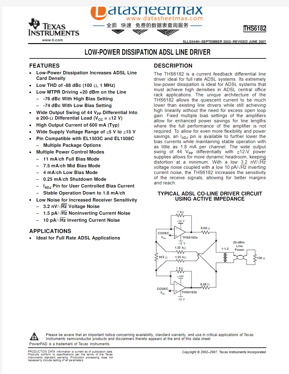
TYPICAL ADSL CO-LINE DRIVER CIRCUIT APPLICATIONS
?
THS6182
SLLS544H–SEPTEMBER2002–REVISED JUNE2007 LOW-POWER DISSIPATION ADSL LINE DRIVER
?Low-Power Dissipation Increases ADSL Line The THS6182is a current feedback differential line Card Density driver ideal for full rate ADSL systems.Its extremely
low-power dissipation is ideal for ADSL systems that ?Low THD of-88dBc(100?,1MHz)
must achieve high densities in ADSL central office ?Low MTPR Driving+20dBm on the Line
rack applications.The unique architecture of the –-76dBc With High Bias Setting THS6182allows the quiescent current to be much
lower than existing line drivers while still achieving –-74dBc With Low Bias Setting
high linearity without the need for excess open loop ?Wide Output Swing of44V PP Differential Into
gain.Fixed multiple bias settings of the amplifiers a200-?Differential Load(V CC=±12V)
allow for enhanced power savings for line lengths ?High Output Current of600mA(Typ)where the full performance of the amplifier is not
required.To allow for even more flexibility and power ?Wide Supply Voltage Range of±5V to±15V
savings,an I ADJ pin is available to further lower the ?Pin Compatible with EL1503C and EL1508C
bias currents while maintaining stable operation with –Multiple Package Options as little as 1.8mA per channel.The wide output
swing of44V PP differentially with±12-V power ?Multiple Power Control Modes
supplies allows for more dynamic headroom,keeping –11mA/ch Full Bias Mode
distortion at a minimum.With a low 3.2nV/√Hz –7.5mA/ch Mid Bias Mode voltage noise coupled with a low10pA/√Hz inverting
–4mA/ch Low Bias Mode current noise,the THS6182increases the sensitivity
of the receive signals,allowing for better margins –0.25mA/ch Shutdown Mode
and reach.
–I ADJ Pin for User Controlled Bias Current
–Stable Operation Down to1.8mA/ch
USING ACTIVE IMPEDANCE
?Low Noise for Increased Receiver Sensitivity
– 3.2nV/√Hz Voltage Noise
– 1.5pA/√Hz Noninverting Current Noise
–10pA/√Hz Inverting Current Noise
?Ideal for Full Rate ADSL Applications
Please be aware that an important notice concerning availability,standard warranty,and use in critical applications of Texas
Instruments semiconductor products and disclaimers thereto appears at the end of this data sheet.
PowerPAD is a trademark of Texas Instruments.
PRODUCTION DATA information is current as of publication date.Copyright?2002–2007,Texas Instruments Incorporated Products conform to specifications per the terms of the Texas
Instruments standard warranty.Production processing does not
necessarily include testing of all parameters.
https://www.doczj.com/doc/4f18952109.html,
PACKAGE DISSIPATION RATINGS (1)
RECOMMENDED OPERATING CONDITIONS
THS6182
SLLS544H–SEPTEMBER 2002–REVISED JUNE 2007
These devices have limited built-in ESD protection.The leads should be shorted together or the device placed in conductive foam during storage or handling to prevent electrostatic damage to the MOS gates.
ORDERING INFORMATION
PRODUCT
PACKAGE (1)
PACKAGE CODE
SYMBOL
ORDER NUMBER TRANSPORT MEDIA
Tape and reel THS6182RHFR
(3000devices)Leadless 24-pin
THS6182RHF
RHF-24
6182
4,mm x 5,mm PowerPAD?
Tape and reel THS6182RHFT (250devices)THS6182D
Tube (40devices)THS6182D
SOIC-16
D-16
THS6182
Tape and reel THS6832DR (2500devices)THS6182DW
Tube (25devices)THS6182DW
SOIC-20
DW-20
THS6182
Tape and reel THS6182DWR (2000devices)THS6182DWP
Tube (25devices)THS6182DWP SOIC-20PowerPAD
DWP-20
THS6182
Tape and reel THS6182DWPR
(2000devices)
(1)
For the most current package and ordering information,see the Package Option Addendum at the end of this document,or see the TI website at https://www.doczj.com/doc/4f18952109.html, .
PowerPAD SOLDERED (2)
PowerPAD NOT SOLDERED (3)
PACKAGE θJC θJA
θJC
RHF-24(2)
32°C/W 74°C/W 1.7°C/W D-16--62.9°C/W 25.7°C/W DW-20--45.4°C/W 16.4°C/W DWP-20(2)
21.5°C/W
43.9°C/W
0.37°C/W
(1)θJA values shown are typical for standard test PCBs only.
(2)
For high-power dissipation applications,use of the PowerPAD package with the PowerPad on the underside of the chip.This acts as a heatsink and must be connected to a thermally dissipating plane for proper dissipation.Failure to do so may result in exceeding the maximum junction temperature which could permanently damage and/or reduce the lifetime the device.See TI technical brief SLMA002for more information about utilizing the PowerPAD thermally enhanced package.
(3)
Use of packages without the PowerPAD or not soldering the PowerPAD to the PCB,should be limited to low-power dissipation applications.
MIN NOM MAX UNIT
Dual supply ±5±12±15V CC+to V CC-Supply voltage
V
Single supply
10
24
30
2
Submit Documentation Feedback
https://www.doczj.com/doc/4f18952109.html,
ABSOLUTE MAXIMUM RATINGS
ELECTRICAL CHARACTERISTICS
THS6182
SLLS544H–SEPTEMBER 2002–REVISED JUNE 2007
over operating free-air temperature range unless otherwise noted (1)
ELECTRICAL THS6132
V CC Supply voltage ±16.5V V I Input voltage ±V CC I O Output current
1000mA V IO
Differential input voltage
±2V THERMAL Maximum junction temperature,any condition
150°C T J Maximum junction temperature,continuous operation,long term reliability (2)
125°C T stg Storage temperature
65°C to 150°C
ESD
HBM
2000V ESD ratings
CDM 1500V MM
200V
(1)The absolute maximum ratings under any condition is limited by the constraints of the silicon process.Stresses above these ratings may cause permanent damage.Exposure to absolute-maximum-rated conditions for extended periods may degrade device reliability.These are stress ratings only,and functional operation of the device at these or any other conditions beyond those ispecified is not implied.(2)
The maximum junction temperature for continuous operation is limited by package constraints.Operation above this temperature may result in reduced reliability and/or lifetime of the device.
over recommended operating free-air temperature range,T A =25°C,V CC =±12V,R F =2k ?,Gain =+5,I ADJ =Bias1=Bias2=0V,R L =50?(unless otherwise noted)
3
Submit Documentation Feedback
https://www.doczj.com/doc/4f18952109.html,
THS6182
SLLS544H–SEPTEMBER 2002–REVISED JUNE 2007
ELECTRICAL CHARACTERISTICS (continued)
over recommended operating free-air temperature range,T A =25°C,V CC =±12V,R F =2k ?,Gain =+5,I ADJ =Bias1=Bias2=0V,R L =50?(unless otherwise noted)
PARAMETER
TEST CONDITIONS
MIN TYP MAX UNIT
OUTPUT CHARACTERISTICS
R L =100?±3.9±4.1V CC =±5V
V R L =25?±3.7±3.9R L =100?±10.7±11V O
Single-ended output voltage swing
V CC =±12V V R L =25?±10±10.6R L =100?±13.5±13.9V CC =±15V V
R L =25?±12.7±13.4R L =5?
V CC =±5V ±350±400I O Output current
(1)
V CC =±12V ±450±600mA R L =10?V CC =±15V ±450
±600I (SC)
Short-circuit current (1)R L =1?V CC =±12V 1000
mA Output resistance
Open-loop 6?Output resistance—terminate mode f =1MHz,Gain =+100.05?Output resistance—shutdown mode
f =1MHz,Open-loop
8.5
k ?
POWER SUPPLY Dual supply ±4±12±16.5V CC
Operating range
V Single supply 8
2433T A =25°C 9.710.7V CC =±5V
mA T A =full range 11.7Quiescent current (each driver)(2)T A =25°C 1112Full-bias mode (Bias-1=0,V CC =±12V mA Bias-2=0)
T A =full range 12.5(Trimmed with V CC =±12V at 25°C)
I CC
T A =25°C 11.5
12.5V CC =±15V
mA
T A =full range
13Mid;Bias-1-1,Bias-2=0
7.58.5Quiescent current (each driver)Low;Bias-1=0,Bias-2=145mA
Variable bias modes,V CC =±12V
Shutdown;Bias-1=1,Bias-2=10.25
0.9
T A =25°C -50-56V CC =±5V,?V CC =±0.5V T A =full range -47PSRR Power supply rejection ratio
dB
T A =25°C -56-60
V CC =±12V,±15V,?V CC =±1V
T A =full range
-53
DYNAMIC PERFORMANCE
Gain =+1,RF =1.2k ?
100Gain =+2,RF =1k ?80R L =100?
MHz
Gain =+5,RF =1k ?35Gain =+10,RF =1k ?20Single-ended small-signal bandwidth BW
(-3dB),V O =0.1Vrms
Gain =+1,RF =1.5k ?65Gain =+2,RF =1k ?60R L =25?
MHz Gain =+5,RF =1k ?40Gain =+10,RF =1k ?
22SR
Single-ended slew rate
(3)
V O =10V PP ,Gain =+5
450
V/μs (1)A heatsink is required to keep the junction temperature below absolute maximum rating when an output is heavily loaded or shorted.See Absolute Maximum Ratings section for more information.
(2)Approximately 0.5mA (total)flows from V CC+to GND for internal logic control bias.(3)Slew rate is defined from the 25%to the 75%output levels.
4
Submit Documentation Feedback
https://www.doczj.com/doc/4f18952109.html,
THS6182 SLLS544H–SEPTEMBER2002–REVISED JUNE2007
ELECTRICAL CHARACTERISTICS(continued)
over recommended operating free-air temperature range,T A=25°C,V CC=±12V,R F=2k?,
Gain=+5,I ADJ=Bias1=Bias2=0V,R L=50?(unless otherwise noted)
PARAMETER TEST CONDITIONS MIN TYP MAX UNIT DC PERFORMANCE
T A=25°C120 Input offset voltage
T A=full range25
mV
V OS V CC=±5V,±12V,±15V T A=25°C0.510 Differential offset voltage
T A=full range15 Offset drift T A=full range50μV/°C
T A=25°C815 -Input bias current
T A=full range20
I IB V CC=±5V,±12V,±15VμA
T A=25°C815 +Input bias current
T A=full range20
Z OL Open loop transimpedance R L=1k?,V CC=±12V,±15V900k?INPUT CHARACTERISTICS
T A=25°C±2.7±3
V CC=±5V V
T A=full range±2.6
T A=25°C±9.5±9.8
V ICR Input common-mode voltage range V CC=±12V V
T A=full range±±9.3
T A=25°C±12.4±12.7
V CC=±15V V
T A=full range±12.1
T A=25°C4854
CMRR Common-mode rejection ratio V CC=±5V,±12V,±15V dB
T A=full range44
+Input800k?
R I Input resistance
-Input30?
C i Input capacitance 1.7pF LOGIC CONTROL CHARACTERISTICS
V IH Bias pin voltage for logic12
Relative to GND pin voltage V
V IL Bias pin voltage for logic00.8
I IH Bias pin current for logic1V IH=3.3V,GND=0V430μA
I IL Bias pin current for logic0V IL=0.5V,GND=0V110μA
Transition time,logic0to logic1(4)1μs
Transition time,logic1to logic0(4)1μs (4)Transition time is defined as the time from when the logic signal is applied to the time when the supply current has reached half its final
value.
LOGIC TABLE(1)(2)
BIAS-1BIAS-2FUNCTION DESCRIPTION
00Full bias mode Amplifiers ON with lowest distortion possible(default state)
10Mid bias mode Amplifiers ON with power savings with a reduction in distortion performance
01Low bias mode Amplifiers ON with enhanced power savings and a reduction of distortion performance 11Shutdown mode Amplifiers OFF and output has high impedance
(1)The default state for all logic pins is a logic zero(0).
(2)The GND pin useable range is from V CC-to(V CC+-4V).
5
Submit Documentation Feedback
https://www.doczj.com/doc/4f18952109.html,
100?
R G
PIN ASSIGNMENTS
D1 IN?
D1 OUT
V?
GND
GND
GND
GND
D1 IN+
BIAS?2
BIAS?1
D2 IN?
D2 OUT
GND
GND
GND
GND
D2 IN+
I ADJ
N/C
THS6182
SOIC?20 (DW) AND
SOIC?20 PowerPAD? (DWP) PACKAGES
D1 IN?
D1 OUT
V CC?
GND
GND
D1 IN+
BIAS?2
BIAS?1
D2 IN?
D2 OUT
V CC+
GND
GND
D2 IN+
I ADJ
N/C
THS6182
SOIC?16 (D) PACKAGE
(TOP VIEW)
V
N/C
V CC+
N/C
N/C
N/C
N/C
GND
THS6182
Leadless 24?pin PowerPAD?
4 mm X
5 mm (RHF) PACKAGE
(TOP VIEW)
B
I
A
S
?
B
I
A
S
?
D
1
I
N
I
A
D
D
2
I
N
V CC+
CC
THS6182
SLLS544H–SEPTEMBER2002–REVISED JUNE2007
Figure1.Single-Supply ADSL CO Line Driver Circuit Utilizing Active Impedance(SF=4)
A.The PowerPAD is electrically isolated from all active circuity and pins.Connection of the PowerPAD to the PCB
ground plane is highly recommended,although not required,as this plane is typically the largest copper plane on a
PCB.The thermal performance will be better with a large copper plane than a small one.
6Submit Documentation Feedback
https://www.doczj.com/doc/4f18952109.html,
TYPICAL CHARACTERISTICS
Table of Graphs
?90
?80?70?60?50?40?30?20?100C r o s s t a l k ?d B
100 k
1 M
10 M
100 M
f ? Frequency ? Hz
00.5
1.5
2
2.5
200
400
600
800
O ut p ut Cur r ent ?mA
O u t p u t V o l t a g e H e a d r o o m ?(V C C ?V o u t )
010
203040506070
80C M R R ?d B
10 k
100 k
1 M
10 M
100 M
f ? Frequency ? Hz
THS6182
SLLS544H–SEPTEMBER 2002–REVISED JUNE 2007
FIGURE
Output voltage headroom vs Output current 2Common-mode rejection ratio vs Frequency 3Crosstalk
vs Frequency 4Total quiescent current 5Large signal output amplitude vs Frequency 6-8Voltage and current noise vs Frequency
9Overdrive recovery 10Power supply rejection ratio vs Frequency 11Output amplitude vs Frequency 12-37Slew rate
vs Output voltage 38Closed-loop output impedance vs Frequency 39vs Supply voltage 40Quiescent current
vs Temperature
41Common-mode rejection ratio vs Common-mode voltage 42Input bias current vs Temperature 43Input offset voltage vs Temperature 442nd Harmonic distribution vs Frequency 45-523rd Harmonic distribution vs Frequency 53-602nd Harmonic distribution vs Output voltage 61-643rd Harmonic distribution
vs Output voltage
65-68
COMMON-MODE REJECTION
OUTPUT VOLTAGE HEADROOM
RATIO CROSSTALK
vs
vs
vs
OUTPUT CURRENT
FREQUENCY
FREQUENCY
Figure 2.Figure 3.Figure 4.
7
Submit Documentation Feedback
https://www.doczj.com/doc/4f18952109.html,
05
10
15
20
25
0.01
0.11
10
100
Rs et t o GND k
T o t a l Q u i e s c e n t C u r r e n t (m A )?
??
??2L a r g e S i g n a l O u t p u t A m p l i t u d e ?d B (V P P )
f ? Frequency ? Hz
?18
?12?60612182430f L a r g e S i g n a l O u t p u t A m p l i t u d e ?d B (V P P )
100 k
1 M
10 M 100 M
1 G
f ? Frequency ? Hz
10
1001000
110
100
1000
? V o l t a g e N o i s e ?n V /
H z V n f ? Frequency ? Hz
? C u r r e n t N o i s e ?p A /
H z
I n
?3?2?0230.0
0.51.0
Tim e (S )
15
105
I n p u t V o l t a g e ?V
O u t p u t V o l t a g e ?V
μ
?18?12?6
6
12
18L a r g e S i g n a l O u t p u t A m p l i t u d e ?d B (V P P )
f ? Frequency ? Hz
?6
?4?3?202 f ? Frequency ? Hz
O u t p u t A m p l i t u d e ?d B
100 k
1 M
10 M 100 M 1 G
f ? Frequency ? Hz
O u t p u t A m p l i t u d e ?d B
100 k
1 M 10 M 100 M 1 G
?10010203040506070801k
f ?Frequency ?Hz
P S S R ?P o w e r S u p p l y R e j e c t i o n R a t i o ?d B
10k
100k 1M 10M
100M
THS6182
SLLS544H–SEPTEMBER 2002–REVISED JUNE 2007
LARGE SIGNAL OUTPUT
LARGE SIGNAL OUTPUT
AMPLITUDE
AMPLITUDE
vs
vs
TOTAL QUIESCENT CURRENT
FREQUENCY
FREQUENCY
Figure 5.
Figure 6.Figure 7.
LARGE SIGNAL OUTPUT
AMPLITUDE
VOLTAGE AND CURRENT NOISE
vs
vs
FREQUENCY
FREQUENCY
OVERDRIVE RECOVERY
Figure 8.
Figure 9.Figure 10.
POWER SUPPLY REJECTION
RATIO OUTPUT AMPLITUDE
OUTPUT AMPLITUDE
vs
vs
vs
FREQUENCY
FREQUENCY
FREQUENCY
Figure 11.Figure 12.Figure 13.
8
Submit Documentation Feedback
https://www.doczj.com/doc/4f18952109.html,
20 f ? Frequency ? Hz
O u t p u t A m p l i t u d e ?d B
100 k
1 M
10 M 100 M
7
8
9
1012131416 f ? Frequency ? Hz
O u t p u t A m p l i t u d e ?d B
100 k 1 M 10 M 100 M 1 G
f ? Frequency ? Hz
O u t p u t A m p l i t u d e ?d B
100 k
1 M
10 M
100 M
f ? Frequency ? Hz
O u t p u t A m p l i t u d e ?d B
100 k
1 M 10 M 100 M
12 f ? Frequency ? Hz
O u t p u t A m p l i t u d e ?d B
02
f ? Frequency ? Hz
O u t p u t A m p l i t u d e ?d B
100 k
1 M 10 M 100 M 1 G
2345678910 f ? Frequency ? Hz
O u t p u t A m p l i t u d e ?d B
100 k
1 M 10 M 100 M 1 G
f ? Frequency ? Hz
O u t p u t A m p l i t u d e ?d B
f ? Frequency ? Hz
0369
12
O u t p u t A m p l i t u d e ?d B
100 k
1 M
10 M
100 M
1 G
THS6182
SLLS544H–SEPTEMBER 2002–REVISED JUNE 2007
OUTPUT AMPLITUDE
OUTPUT AMPLITUDE
OUTPUT AMPLITUDE
vs
vs
vs
FRQUENCY
FREQUENCY
FREQUENCY
Figure 14.Figure 15.Figure 16.OUTPUT AMPLITUDE
OUTPUT AMPLITUDE
OUTPUT AMPLITUDE
vs
vs
vs
FREQUENCY
FREQUENCY
FREQUENCY
Figure 17.Figure 18.Figure 19.OUTPUT AMPLITUDE
OUTPUT AMPLITUDE
OUTPUT AMPLITUDE
vs
vs
vs
FREQUENCY
FREQUENCY
FREQUENCY
Figure 20.Figure 21.Figure 22.
9
Submit Documentation Feedback
https://www.doczj.com/doc/4f18952109.html,
7
8
9
10111213141516 f ? Frequency ? Hz
O u t p u t A m p l i t u d e ?d B
100 k
1 M 10 M 100 M
O u t p u t A m p l i t u d e ?d
B
7
89 f ? Frequency ? Hz
100 k
1 M 10 M 100 M
7
8
910111213141516 f ? Frequency ? Hz
O u t p u t A m p l i t u d e ?d B
7
8910111213141516 f ? Frequency ? Hz
O u t p u t A m p l i t u d e ?d B
100 k
1 M 10 M 100 M
f ? Frequency ? Hz
100 k
1 M 10 M 100 M
20 f ? Frequency ? Hz
O u t p u t A m p l i t u d e ?d B
f ? Frequency ? Hz
O u t p u t A m p l i t u d e ?d B
7
8
91012131416 f ? Frequency ? Hz
O u t p u t A m p l i t u d e ?d B
100 k 1 M 10 M 100 M
f ? Frequency ? Hz
O u t p u t A m p l i t u d e ?d B
100 k
1 M 10 M 100 M
THS6182
SLLS544H–SEPTEMBER 2002–REVISED JUNE 2007
OUTPUT AMPLITUDE
OUTPUT AMPLITUDE
OUTPUT AMPLITUDE
vs
vs
vs
FREQUENCY
FREQUENCY
FREQUENCY
Figure 23.Figure 24.Figure 25.OUTPUT AMPLITUDE
OUTPUT AMPLITUDE
OUTPUT AMPLITUDE
vs
vs
vs
FREQUENCY
FREQUENCY
FREQUENCY
Figure 26.Figure 27.Figure 28.OUTPUT AMPLITUDE
OUTPUT AMPLITUDE
OUTPUT AMPLITUDE
vs
vs
vs
FREQUENCY
FREQUENCY
FREQUENCY
Figure 29.Figure 30.Figure 31.
10
Submit Documentation Feedback
https://www.doczj.com/doc/4f18952109.html,
?6?4?3?2023 f ? Frequency ? Hz
O u t p u t A m p l i t u d e ?d B
100 k
1 M
10 M 100 M
1 G
0123 f ? Frequency ? Hz O u t p u t A m p l i t u d e ?d B
f ? Frequency ? Hz
O u t p u t A m p l i t u d e ?d B
100 k
1 M
10 M
100 M
7
8
9 f ? Frequency ? Hz O u t p u t A m p l i t u d e ?d B
100 k 1 M
10 M
100 M
f ? Frequency ? Hz
O u t p u t A m p l i t u d e ?d B
100 k
1 M
10 M
100 M
f ? Frequency ? Hz
O u t p u t A m p l i t u d e ?d B
100 k
1 M
10 M
100 M
0.0110
1001000
f ? Frequency ? Hz
Z o ?C l o s e d L o o p O u t p u t I m p e d a n c e ?O h m s
0200
300
400
500
5101520
Output Voltage ? Vp?p
S l e w ?R a i e (V /u s
)
20
Supply Voltage ? +/?Vcc
T o t a l Q u i e s c e n t C u r r e n t ?m A
THS6182
SLLS544H–SEPTEMBER 2002–REVISED JUNE 2007
OUTPUT AMPLITUDE
OUTPUT AMPLITUDE
OUTPUT AMPLITUDE
vs
vs
vs
FREQUENCY
FREQUENCY
FREQUENCY
Figure 32.Figure 33.Figure 34.OUTPUT AMPLITUDE
OUTPUT AMPLITUDE
OUTPUT AMPLITUDE
vs
vs
vs
FREQUENCY
FREQUENCY
FREQUENCY
Figure 35.Figure 36.
Figure 37.
CLOSED LOOP OUTPUT
SLEW RATE
IMPEDANCE
QUIESCENT CURRENT
vs
vs
vs
OUTPUT VOLTAGE
FREQUENCY
SUPPLY VOLTAGE
Figure 38.Figure 39.Figure 40.
11
Submit Documentation Feedback
https://www.doczj.com/doc/4f18952109.html,
20
30405060
70
8090
Common?Mode Voltage ? V
C o m m o n ?M o d e R e j e c t i o n R a t i o ?d
B
6789101213
Temperature ? Deg C
I n p u t B i a s C u r r e n t ?u A
?40
?20
020*********
05
10
20
25
Temperature ? Deg.C
T o t a l Q u i e s c e n t C u r r e n t ?m A
33.5
4
4.5
5
Temperature ? Deg C
I n p u t O f f s e t V o l t a g e ?m V
?90
?80
?60
?40
f ? Frequency ? Hz
2n d H D ?d B c
100 k
1 M 10 M 100 M
?90?80
?60
?40
f ? Frequency ? Hz
2n d H D ?d B c
100 k
1 M 10 M 100 M
?80
?60 f ? Frequency ? Hz
2n d H D ?d B c
?90?80
?60?40
f ? Frequency ? Hz
2n d H D ?d B c
100 k
1 M 10 M 100 M
f ? Frequency ? Hz
2n d H D ?d B c
100 k
1 M
10 M
100 M
THS6182
SLLS544H–SEPTEMBER 2002–REVISED JUNE 2007
QUIESCENT CURRENT
COMMON-MODE REJECTION RATIO
INPUT BIAS CURRENT
vs
vs
vs
TEMPERATURE
COMMON-MODE VOLTAGE
TEMPERATURE
Figure 41.
Figure 42.
Figure 43.
INPUT OFFSET VOLTAGE
2ND HARMONIC DISTORTION
2ND HARMONIC DISTORTION
vs
vs
vs
TEMPERATURE
FREQUENCY
FREQUENCY
Figure 44.
Figure 45.
Figure 46.
2ND HARMONIC DISTORTION
2ND HARMONIC DISTORTION
2ND HARMONIC DISTORTION
vs
vs
vs
FREQUENCY
FREQUENCY
FREQUENCY
Figure 47.Figure 48.Figure 49.
12
Submit Documentation Feedback
https://www.doczj.com/doc/4f18952109.html,
?80?60
f ? Frequency ? Hz
2n d H D ?d B c
?80?60 f ? Frequency ? Hz
2n d H D ?d B c
100 k
1 M 10 M 100 M
f ? Frequency ? Hz
2n d H D ?d B c
100 k
1 M 10 M 100 M
f ? Frequency ? Hz
3r d H D ?d B c
100 k
1 M 10 M 100 M
?90
?80?60?40?30
f ? Frequency ? Hz
3r d H D ?d B c
100 k
1 M 10 M 100 M
?90?80?60
?40?30
f ? Frequency ? Hz
3r d H D ?d B c
100 k
1 M 10 M 100 M
f ? Frequency ? Hz
3r d H D ?d B c
100 k
1 M 10 M 100 M
f ? Frequency ? Hz
3r d H D ?d B c
100 k
1 M 10 M 100 M
?90?80?70?60?40?30
f ? Frequency ? Hz
3r d H D ?d B c
100 k
1 M 10 M 100 M
THS6182
SLLS544H–SEPTEMBER 2002–REVISED JUNE 2007
2ND HARMONIC DISTORTION
2ND HARMONIC DISTORTION
2ND HARMONIC DISTORTION
vs
vs
vs
FREQUENCY
FREQUENCY
FREQUENCY
Figure 50.
Figure 51.
Figure 52.
3RD HARMONIC DISTORTION
3RD HARMONIC DISTORTION
3RD HARMONIC DISTORTION
vs
vs
vs
FREQUENCY
FREQUENCY
FREQUENCY
Figure 53.
Figure 54.
Figure 55.
3RD HARMONIC DISTORTION
3RD HARMONIC DISTORTION
3RD HARMONIC DISTORTION
vs
vs
vs
FREQUENCY
FREQUENCY
FREQUENCY
Figure 56.Figure 57.Figure 58.
13
Submit Documentation Feedback
https://www.doczj.com/doc/4f18952109.html,
f ? Frequency ? Hz
3r d H D ?d B c
?90?80
5
101520253035
40
Output Voltage ? Vpp
2n d H D ?d B c
f ? Frequency ? Hz
3r d H D ?d B c
100 k
1 M
10 M
100 M
?90
?80
5
10
Output Voltage ? Vpp
2n d H D ?d B c
Output Voltage ? Vpp
2n d H D ?d B
c
?800
5
10152025
30
?80
2
4
6
8
10
Output Voltage ? Vpp
2n d H D ?d B c
?90
?80
5
101520253035
40
Output Voltage ? Vpp
3r d H D ?d B c
2
4
6
8
10
Output Voltage ? Vpp
3r d H D ?d B c
5
10
15
20
25
30
Output Voltage ? Vpp
3r d H D ?d B c
THS6182
SLLS544H–SEPTEMBER 2002–REVISED JUNE 2007
3RD HARMONIC DISTORTION
3RD HARMONIC DISTORTION
2ND HARMONIC DISTORTION
vs
vs
vs
FREQUENCY
FREQUENCY
OUTPUT VOLTAGE
Figure 59.
Figure 60.
Figure 61.
2ND HARMONIC DISTORTION
2ND HARMONIC DISTORTION
2ND HARMONIC DISTORTION
vs
vs
vs
OUTPUT VOLTAGE
OUTPUT VOLTAGE
OUTPUT VOLTAGE
Figure 62.
Figure 63.
Figure 64.
3RD HARMONIC DISTORTION
3RD HARMONIC DISTORTION
3RD HARMONIC DISTORTION
vs
vs
vs
OUTPUT VOLTAGE
OUTPUT VOLTAGE
OUTPUT VOLTAGE
Figure 65.Figure 66.Figure 67.
14
Submit Documentation Feedback
https://www.doczj.com/doc/4f18952109.html,
?90
?800
2
46
8
10
Output Voltage ? Vpp
3r d H D ?d B c
THS6182
SLLS544H–SEPTEMBER 2002–REVISED JUNE 2007
3RD HARMONIC DISTORTION
vs
OUTPUT VOLTAGE
Figure 68.
15
Submit Documentation Feedback
https://www.doczj.com/doc/4f18952109.html,
APPLICATION INFORMATION
DEVICE PROTECTION FEATURE
THERMAL INFORMATION
Side View (a)
End View (b)
Bottom View (c)
DIE
Thermal Pad
THS6182
SLLS544H–SEPTEMBER 2002–REVISED JUNE 2007
The THS6182contains two independent operational amplifiers.These amplifiers are current feedback topology amplifiers made for high-speed operation.They have been specifically designed to deliver the full power requirements of ADSL and therefore can deliver output currents of at least 400mA at full output voltage.The THS6182is fabricated using Texas Instruments 30-V complementary bipolar process,HVBiCOM.This process provides excellent isolation and high slew rates that result in the device's excellent crosstalk and extremely low distortion.
The THS6182has a built-in thermal protection feature.Should the internal junction temperature rise above approximately 160°C,the device automatically shuts down.Such a condition could exist with improper heat sinking or if the output is shorted to ground.When the abnormal condition is fixed,the internal thermal shutdown circuit automatically turns the device back on.This occurs at approximately 145°C,junction temperature.Note that the THS6182does not have short-circuit protection and care should be taken to minimize the output current below the absolute maximum ratings.
The THS6182is available in a thermally-enhanced DWP and RHF package,which is a member of the PowerPAD family of packages.This package is constructed using a downset leadframe upon which the die is mounted [see Figure 69(a)and Figure 69(b),for the DWP package example].This arrangement results in the lead frame as a on the underside of the package [see Figure 69(c)].Because this thermal pad has direct thermal contact with the die,excellent thermal performance by providing a good thermal path away from the thermal pad.Note that the PowerPAD is electronically isolated from the active circuitry and any pins.Thus,the PowerPAD can be connected to any potential voltage within the absolute maximum voltage range.Ideally,connection of the PAD to the ground plane is preferred as the plane typically is the largest copper plane on a PCB.
The PowerPAD package allows for both assembly and thermal management in one manufacturing operation.During the surface-mount solder operation (when the leads are being soldered),the thermal pad can also be soldered to a copper area underneath the package.Through the use of thermal paths within this copper area,heat can be conducted away from the package into either a ground plane or other heat dissipating device.This is discussed in more detail in the PCB design considerations section of this document.
The PowerPAD package represents a breakthrough in combining the small area and ease of assembly of surface mount with the,heretofore,awkward mechanical methods of heatsinking.
A.The thermal pad is electrically isolated from all terminals in the package.
Figure 69.Views of Thermally Enhanced DWP Package
16
Submit Documentation Feedback
https://www.doczj.com/doc/4f18952109.html,
RECOMMENDED FEEDBACK AND GAIN RESISTOR VALUES OFFSET
VOLTAGE
NOISE CALCULATIONS
THS6182
SLLS544H–SEPTEMBER2002–REVISED JUNE2007
APPLICATION INFORMATION(continued)
As with all current feedback amplifiers,the bandwidth of the THS6182is an inversely proportional function of the value of the feedback resistor.The recommended resistors with a±12-V power supply for the optimum frequency response with a25-?load system is1k?for a gain of5.These should be used as a starting point and once optimum values are found,1%tolerance resistors should be used to maintain frequency response characteristics.
Consistent with current feedback amplifiers,increasing the gain is best accomplished by changing the gain resistor,not the feedback resistor.This is because the bandwidth of the amplifier is dominated by the feedback resistor value and internal dominant-pole capacitor.The ability to control the amplifier gain independently of the bandwidth constitutes a major advantage of current feedback amplifiers over conventional voltage feedback amplifiers.
It is important to realize the effects of the feedback resistance on distortion.Increasing the resistance decreases the loop gain and increases the distortion.It is also important to know that decreasing load impedance increases total harmonic distortion(THD).Typically,the third order harmonic distortion increases more than the second order harmonic distortion.
Finally,in a differential configuration as shown in Figure1,it is important to note that there is a differential gain and a common-mode gain which are different other.Differentially,the gain is at1+R F/R G.While common-mode gain=1due to R G being connected directly between each amplifier and not to ground.This can lead to potential problems as the stability of the amplifier is determined by R F.Thus,R F must be large enough to ensure the common-mode stability,even though a large differential gain may be required.
The output offset voltage,(V OO)is the sum of the input offset voltage(V IO)and both input bias currents(I IB) times the corresponding gains.The following schematic and formula can be used to calculate the output offset voltage:
Figure70.Output Offset Voltage Model
Noise can cause errors on very small signals.This is especially true for the amplifying small signals.The noise model for current feedback amplifiers(CFB)is the same as voltage feedback amplifiers(VFB).The only difference between the two is that the CFB amplifiers generally specify different current noise parameters for each input while VFB amplifiers usually only specify one noise current parameter.The noise model is shown in Figure71.This model includes all of the noise sources as follows:
?e n=Amplifier internal voltage noise(nV/√Hz)
?IN+=Noninverting current noise(pA/√Hz)
?IN-=Inverting current noise(pA/√Hz)
?e RX=Thermal voltage noise associated with each resistor(e RX=4kTR x)
17
Submit Documentation Feedback
https://www.doczj.com/doc/4f18952109.html,
e ni
e no
e
ni +
ǒe n ǔ2
)ǒIN ) R S ǔ2
)ǒIN– ǒR F ?R G
ǔǔ
2
)4kTR s )4kT ǒR F ?R
G
ǔ
?
Where:
k = Boltzmann’s constant = 1.380658 × 10?23
T = T emperature in degrees Kelvin (273 +°C)R F || R G = Parallel resistance of R F and R G
e no +e ni A V +e ni ǒ1)R
F R G
ǔ
(Noninverting Case)
DRIVING A CAPACITIVE LOAD
THS6182
SLLS544H–SEPTEMBER 2002–REVISED JUNE 2007
APPLICATION INFORMATION (continued)
Figure 71.Noise Model
The total equivalent input noise density (e ni )is calculated by using the following equation:
To get the equivalent output noise of the amplifier,just multiply the equivalent input noise density (e ni )by the overall amplifier gain (A V ).
As the previous equations show,to keep noise at a minimum,small value resistors should be used.As the
closed-loop gain is increased (by reducing R G ),the input noise is reduced considerably because of the parallel resistance term.
Driving capacitive loads with high performance amplifiers is not a problem as long as certain precautions are taken.The first is to realize that the THS6182has been internally compensated to maximize its bandwidth and slew rate performance.When the amplifier is compensated in this manner,capacitive loading directly on the output will decrease the device's phase margin leading to high frequency ringing or oscillations.Therefore,for capacitive loads of greater than 10pF,it is recommended that a resistor be placed in series with the output of the amplifier,as shown in Figure 72.A minimum value of 2?should work well for most applications.For example,in 75-?setting the series resistor value to 75?both isolates any capacitance loading and provides the proper line impedance matching at the source end.
18
Submit Documentation Feedback
https://www.doczj.com/doc/4f18952109.html,
1 k ?
Input
Output PCB DESIGN CONSIDERATIONS
THS6182
SLLS544H–SEPTEMBER 2002–REVISED JUNE 2007
APPLICATION INFORMATION (continued)
Figure 72.Driving a Capacitive Load
Proper PCB design techniques in two areas are important to assure proper operation of the THS6182.These areas are high-speed layout techniques and thermal-management techniques.Because the THS6182is a high-speed part,the following guidelines are recommended.
?Ground plane -It is essential that a ground plane be used on the board to provide all components with a low inductive ground connection.Although a ground connection directly to a terminal of the THS6012is not necessarily required,it is recommended that the thermal pad of the package be tied to ground.This serves two functions.It provides a low inductive ground to the device substrate to minimize internal crosstalk and it provides the path for heat removal.Note that the BiCom process is a SOI process and thus,the substrate is isolated from the active circuitry.
?Input stray capacitance -To minimize potential problems with amplifier oscillation,the capacitance at the inverting input of the amplifiers must be kept to a minimum.To do this,PCB trace runs to the inverting input must be as short as possible,the ground plane should be removed under any etch runs connected to the inverting input,and external components should be placed as close as possible to the inverting input.This is especially true in the noninverting configuration.
?Proper power supply decoupling -Use a minimum of a 6.8-μF tantalum capacitor in parallel with a 0.1-μF ceramic capacitor on each supply terminal.It may be possible to share the tantalum among several amplifiers depending on the application,but a 0.1-μF ceramic capacitor should always be used on the supply terminal of every amplifier.In addition,the 0.1-μF capacitor should be placed as close as possible to the supply terminal.As this distance increases,the inductance in the connecting etch makes the capacitor less effective.The designer should strive for distances of less than 0.1inches between the device power terminal and the ceramic capacitors.
?For a differential configuration as shown in Figure 1,it is recommended that a 0.1-μF or 1-μF capacitor be added across the power supplies (from V CC+to V CC-)as close as possible to the THS6182.This allows for differential currents to flow properly,signficantly reducing even-order harmonic distortion.The 0.1-μF capacitors to ground should also be used as previously stipulated.Because of its power dissipation,proper thermal management of the THS6182is required.Although there are many ways to properly heatsink this device,the following steps illustrate one recommended approach for a multilayer PCB with an internal ground plane utilizing the 20pin DWP PowerPAD package.
1.Prepare the PCB with a top side etch pattern as shown in Figure 73.There should be etch for the leads as well as etch for the thermal pad.
2.Place 18holes in the area of the thermal pad.These holes should be 13mils in diameter.They are kept small so that solder wicking through the holes is not a problem during reflow.
3.It is recommended,but not required,to place six more holes under the package,but outside the thermal pad area.These holes are 25mils in diameter.They may be larger because they are not in the area to be soldered so that wicking is not a problem.
4.Connect all 24holes,the 18within the thermal pad area and the 6outside the pad area,to the internal ground plane.
5.When connecting these holes to the ground plane,do not use the typical web or spoke via connection methodology.Web connections have a high thermal resistance connection that is useful for slowing the
19
Submit Documentation Feedback
https://www.doczj.com/doc/4f18952109.html,
PowerPAD and via placement pad area (0.085 x 0.120) with 15vias (Via diameter = 0.013)
Vias should go through the board connecting the top layer
PowerPad to any and all ground planes. (The larger the ground
plane, the larger the area to distribute the heat.) Solder resist should be used on the bottom side ground plane in order to prevent wicking of the solder through the vias during the reflow process.
All Units in Inches
THS6182
SLLS544H–SEPTEMBER 2002–REVISED JUNE 2007
APPLICATION INFORMATION (continued)
heat transfer during soldering operations.This makes the soldering of vias that have plane connections easier.However,in this application,low thermal resistance is desired for the most efficient heat transfer.Therefore,the holes under the THS6182package should make their connection to the internal ground plane with a complete connection around the entire circumference of the plated through hole.
6.The top-side solder mask should leave exposed the terminals of the package and the thermal pad area with its five holes.The four larger holes outside the thermal pad area,but still under the package,should be covered with solder mask.
7.Apply solder paste to the exposed thermal pad area and all of the operational amplifier terminals.
8.With these preparatory steps in place,the THS6182DWP is simply placed in position and run through the solder reflow operation as any standard surface-mount component.This results in a part that is properly installed.
Figure 73.20-Pin DWP PowerPAD PCB Etch and Via Pattern
The RHF package is similar to the DWP package with respect to PCB mounting procedures.The recommended PCB layout is as shown in Figure 74.
20
Submit Documentation Feedback
二硫化碳危险化学品安全技术说明书 一、化学品及企业标识 化学品中文名称:二硫化碳 化学品俗名或商品名:CS 2 化学品英文名称:Carbon disulfide 二、成分/组成信息 纯品√混合物□ 化学名称:二硫化碳 有害物成分浓度 CAS NO. 100% 75-15-0 CS 2 三、危险性概述 危险性类别:第3.1类,低闪点易燃液体 侵入途径:通过呼吸道进入及皮肤接触两种途径。 健康危害:短时吸入本品浓度在10000mg/m3以上者,可发生严重急性中毒;接触浓度为3000~5000mg/m3时可引起急性中毒;成人最小致死量为10ml,二硫化碳蒸气吸入主要影响神经、心血管和生殖系统。 环境危害:因其蒸气密度为空气的3倍,污染时贴地面扩散;二硫化碳是一种甲B类可燃液体,易挥发。 燃爆危险:二硫化碳是危害性最大的物质之一,从消防角度来看,它具有全部危害性,它是一种易燃、易爆、高毒、高挥发性液体(常温下),可产生静电荷而起爆,不能与电荷或火花、高温接触。 四、急救措施 皮肤接触:皮肤接触到本品,应立即脱去污染的衣着,用肥皂水及清水冲洗干净。 眼睛接触:眼睛如接触到本品后应立即提起眼睑,先用水清洗眼部,避免揉搓,进行彻底冲洗。 吸入:吸入本品迅速脱离现场至空气新鲜处,呼吸困难时及时输氧,呼吸停止时,立即进行人口呼吸及心脏压迫。 食入:误食入本品后,充分漱口、饮水、洗胃、就医。 五、消防措施 危险特性:其蒸气与空气形成爆炸性混合物,遇明火、高温极易燃烧爆炸,
与氧化剂能发生强烈反应,其蒸气比空气重,能在较低处扩散到相当远的地方,遇火源引着回燃。若遇高温,容器内压力增大,有开裂和爆炸的危险。高速冲击、流动、激荡后可产生静电,静电放电可引起燃烧爆炸,二硫化碳含量在(V%):4~8%时,爆炸威力最大,二硫化碳爆炸时的最大压力为730kpa(7.3atm)。 有害燃烧产物:SO 2、CO 2 灭火方法及灭火剂:用大量水封其泄漏产品,其次用雾状水与泡沫灭火,用砂土掩埋。 灭火注意事项:不能用水冲击燃烧液面;站上风方向;用水扑救二硫化碳应特别小心;由于用水扑救硫化物火灾时,容易生成有高毒的硫化氢气体,因为它比二硫化碳更危险;用二氧化碳和干粉只能灭小部分火灾,用水和干粉并用,则效果会更好。 六、泄漏应急处理 切断电源。污染区人员疏散至安全区,禁止无关人员进入污染区,切断火源,应急处理人员在确保安全的情况下,穿戴好劳保用品,进行堵漏。喷水雾会减少蒸发,但不能降低泄漏物在受限制空间内的易燃性。用沙土、蛭石或其它惰性材料吸收,然后收集运至废物处理所处理,如大量泄漏用水覆盖二硫化碳表面层,利用挖沟、围堤收容,然后收集转移,回收或无害处理后可废弃。 七、操作处置与储存 操作注意事项:二硫化碳是一种甲B类可燃液体,易挥发。精品二硫化碳在常温下对大部分金属无腐蚀作用;密闭操作,加强通风,操作人员必须经过专门培训,严格遵守操作规程。建议操作人员佩戴自吸过滤式防毒面具(半面罩),戴全封闭式防护眼镜,穿防毒物渗透工作服,戴橡胶耐油手套;粗品二硫化碳含有杂质,它对铜合金有腐蚀;250℃时二硫化碳对钢铁及其它金属有腐蚀,因此在高温下贮存或加工二硫化碳时,必须采用不锈钢材质的设备。常温下,可采用碳钢制圆桶及罐槽贮存二硫化碳。容器内可用水封盖表面,储存于阴凉、通风仓库内,远离火种热源。定期检查是否有泄漏现象;空置二硫化碳容器时,必须经过放空、清洗、用蒸气吹蒸48小时,后再用蒸气置换,直至容器内低于爆炸极限的十分之一后,才能置放于空间或焊接检修;灌装时应注意流速小于3m/s,且要有接地装置,防止静电积聚,搬运时要轻装轻卸,防止包装及容器损坏,配备相应品种和数量的消防器材及泄露应急处理设备,倒空的容器可能残留有害物。 储存注意事项:储存于阴凉、通风库房。远离火种、热源。仓温不宜超过30℃。保持容器密封。应与氧化剂、食用化学品分开存放,切忌混储。采用防爆型照明、通风设施。禁止使用易产生火花的机械设备和工具,储区应备有泄漏应
WI-AD-012物料安全数据表 文件编号 WI-AD-012 中山市成业电子电路板有限公司 版次 A0 作业指导书 页次 1/17 标题:物料安全数据表--32#/42#/68#液压油制订日期 2009年8月1日 物质名称(中英文) 32#/42#/68#液压油 危害性闪点(?):约150-260,视级别而定。 避免产品直接接触皮肤、眼睛等,不得吸入油雾,避免 防护措施 产品咽入。 口服:LD>5ML/KG 皮肤:LD>4ML/KG 急性中毒最严重时,对皮肤仅有轻微刺激,不会引起皮肤敏感,对 眼睛仅有轻微刺激。 产品应放置在清凉、干净、干燥并装有足够通风设施的储运及使用之注意事项地方,远离高温、明火及一切强力氧化剂。 若着火,迅速熄灭明火,防止产生火花,并迅速撤离现 场,灭火适用泡沫剂、二氧化碳、干性化学粉末灭火器, 应急处理方法不可用水灭火。 若溢出,用砂、泥土或木屑,吸收溢出的油,然后移去 安全的区域,事后以大量水冲洗被玷污的地方。 应根据有关法例,正确处理废油,切勿让废油污染泥土废弃处理注意事项及水源,并避免废油接触皮肤。旧桶,不可切割及烧焊, 可交回供应商或交由相关部门做翻新处理。
拟制: 审核: 批准: 文件编号 WI-AD-012 中山市成业电子电路板有限公司 版次 A0 作业指导书 页次 2/17 标题:物料安全数据表—绿色长期防锈剂制订日期 2009年8月1日 物质名称(中英文) 绿色长期防锈剂 化学属性或组份干性树脂、稀释溶剂、防锈添加剂 危险品,液态溢留,混合物温度达到或超过其闪点温度,危险性类别容易着火燃烧,且能聚集静电,引起静电火花。高温易 燃易爆。 外观:浅绿色液体 密度:0.6594 溶点:-95? 理化性质沸点:68.8? 闪点:-23? 有效保护期:12个月(室内) 带异臭,无致癌性,轻刺激性。毒害特性 使用及储存时,应注意:避免与眼睛接触,避免吸入蒸储运及使用之注意事项汽或水雾,保证操作环境空气流通,严禁烟火。 皮肤接触:清水冲洗,情况严重送医院治疗。 眼睛接触: 清水冲洗,情况严重送医院治疗。应急处理方法吸入:吸大量清新空气,纯氧气。 误食:喝大量清水排出或送医院治疗。 灭火材料:泡沫、干粉、二氧化碳、水雾、沙子或泥土消防措施灭火步骤:可用水将着火附近的油桶和表面降温。
物料安全数据表(MSDS) 通用名称: 丙二醇 含量规格: ≥99.5% 包装规格: 215kg/桶 生产商: 查询电话: 8 主要组成: 丙二醇。 性状: 无色、有苦味、略粘稠吸湿的液体。 暴露极限: OSHA:未建立 ACGIH: 未建立 NIOSH :未建立 丙二醇可用作不饱和聚酯树脂的原料,也是增塑剂、表面活性剂、乳化剂和破乳剂的原料。可用作防霉剂、水果催熟剂、防腐剂、防冻剂及烟草保湿剂。毒性和刺激性都非常小,迄今尚未发现受害者。 紧急联系电话 6 致癌性:未被 NTP 、OSHA 及IARC 列为致癌物或潜在致癌物。 皮肤接触: 脱去污染的衣着,用大量流动清水冲洗。 眼睛接触: 提起眼睑,用流动清水或生理盐水冲洗。 吸入: 脱离现场至空气新鲜处。就医。 食入: 饮足量温水,催吐。就医。 危险特性: 遇明火、高热可燃。 有害燃烧产物: 一氧化碳、二氧化碳。
灭火方法:消防人员须佩戴防毒面具、穿全身消防服,在上风向灭火。尽可能将容器从火场移至空旷处。喷水保持火场容器冷却,直至灭火结束。处在火场中的容器若已变色或从安全泄压装置中产生声音,必须马上撤离。用水喷射逸出液体,使其稀释成不燃性混合物,并用雾状水保护消防人员。灭火剂:水、雾状水、抗溶性泡沫、干粉、二氧化碳、砂土。 应急处理:迅速撤离泄漏污染区人员至安全区,并进行隔离,严格限制出入。切断火源。建议应急处理人员戴自给正压式呼吸器,穿防毒服。尽可能切断泄漏源。防止流入下水道、排洪沟等限制性空间。小量泄漏:用砂土、蛭石或其它惰性材料吸收。也可以用大量水冲洗,洗水稀释后放入废水系统。大量泄漏:构筑围堤或挖坑收容。用泵转移至槽车或专用收集器内,回收或运至废物处理场所处置。 操作注意事项:密闭操作,全面通风。操作人员必须经过专门培训,严格遵守操作规程。建议操作人员佩戴自吸过滤式防毒面具(半面罩),戴化学安全防护眼镜,穿防毒 物渗透工作服,戴橡胶手套。远离火种、热源,工作场所严禁吸烟。使用防爆型的通风系统和设备。防止蒸气泄漏到工作场所空气中。避免与氧化剂、还原剂接触。搬运时要轻装轻卸,防止包装及容器损坏。配备相应品种和数量的消防器材及泄漏应急处理设备。倒空的容器可能残留有害物。 储存注意事项:储存于阴凉、通风的库房。远离火种、热源。应与氧化剂、还原剂等分开存放,切忌混储。配备相应品种和数量的消防器材。储区应备有泄漏应急处理设备和合适的收容材料。 职业接触限值 中国MAC(mg/m3):未制定标准 前苏联MAC(mg/m3):7 TLVTN:未制订标准 TLVWN:未制订标准 监测方法: 工程控制:生产过程密闭,全面通风。 呼吸系统防护:空气中浓度超标时,必须佩戴自吸过滤式防毒面具(半面罩)。眼睛防护:戴化学安全防护眼镜。 身体防护:穿防毒物渗透工作服。 手防护:戴防化学品手套。 其他防护:工作现场严禁吸烟。避免长期反复接触。定期体检。注意个人清洁卫生。
NEW FAITH HT-TECH PRINTING LTD生效日期: 2007-7-2第1页,共1页 机油类MSDS (化学品安全数据表) 一.化学品名称: ML-HM68高级抗磨液压油 二、中文名: 润滑油 三、外观与性状: 液体澄清无色透明。 四、燃烧性: xx 五、危险特性: 对皮肤有刺激性。 六、燃烧分解物: 一氧化碳、二氧化碳 七、溶解性: 不溶于水 八、灭火方法: 使用化学干粉,耐醇类泡沫,二氧化碳,砂或泥土灭火,不适用用水喷射灭火。 九、储运注意事项:
容器必须加盖密封,同时防止液体倾倒出来,减少挥发量,避免日光照射,放置于阴凉、干燥、通风处。搬运工人应配戴防腐蚀手套。 十、毒性: 属低等毒类 十一、健康危害: 皮肤接触,最严重对皮肤仅有轻微刺激,并不会引起皮肤敏感,进入眼睛,最严重时对眼睛仅有轻微刺激,呼吸道一吸入油雾,对呼吸道仅有车微刺激,并不会引致呼吸道感染。 十二、皮肤接触: 避免皮肤接触,如触及应脱去被沾污衣物,用清水、肥皂洗净受污皮肤,如有刺激感,送医治疗。 十三、眼睛接触: 避免接触眼睛,如触及应张开眼皮,以洁净清水冲洗,如刺激感持续,立即送医治疗。 十四、吸入: 避免吸入油雾,如吸入后有眩晕或恶心感,立即将受害人移到新鲜空气处,如症状持续,马上送医治疗,如受害人呼吸停止,进行人工呼吸。 十五、食入: 避免咽入,如发生可用机械的方法诱发呕吐,如大量入肚确感不适,送医治疗。 十六、防护措施: ①工程控制: 使用时,加强通风。
②呼吸系统防护: 空气中浓度较高时,佩戴防毒口罩。 ③其它: 工作现场严禁吸烟。工作后,沐浴更衣。定期体检。 十七、泄漏处置: 防止火花产生,除处理备油人员外,从速撤离现场,避免吸入油雾,小量溢出,用砂或泥土吸收溢油,然后移至安全地点,根据有关法例处理,后以大量水冲冼被沾污的地方,大量溢出,用砂或泥土截溢油蔓延,防止溢油流入下水道,如有可能,将溢油以槽罐截起,随后处理,或按“小量溢”之方法处理。 十八、废弃处理: 废油处理,应根据有关法例,正确处理废油,切勿让废油污染泥土及水源;废油或被污染物交政府许可证单位处理。旧桶处理,仍可用的旧桶,可交回供应商处理,但请勿除去旧桶上的标签;不可在旧桶内加压;不可将旧桶切割或烧掉;旧桶再用时,必须先除去或清除原有标签。 编写: 审核: 批准: 受控印章:
Safety is the goal, prevention is the means, and achieving or realizing the goal of safety is the basic connotation of safety prevention. (安全管理) 单位:___________________ 姓名:___________________ 日期:___________________ 二硫化碳危险特性及安全注意事 项(最新版)
二硫化碳危险特性及安全注意事项(最新版)导语:做好准备和保护,以应付攻击或者避免受害,从而使被保护对象处于没有危险、不受侵害、不出现事故的安全状态。显而易见,安全是目的,防范是手段,通过防范的手段达到或实现安全的目的,就是安全防范的基本内涵。 (一)危险特性 1、易燃性:易挥发出足以与空气形成可燃混和物的蒸汽,其着火所需能量极小,遇火、过热、流速过快以及和氧化剂接触等都有发生燃烧的危险。受热分解产生有毒的硫化物烟气。燃烧会产生一氧化碳、二氧化硫、二氧化碳等有毒气体,而且具有回燃的特点。 注:液体的闪点、沸点和自燃点越低,蒸汽压越大,发生着火燃烧的危险性也越大。 2、爆炸性:当挥发出的蒸汽与空气形成的混合气体达到爆炸极限浓度(1.3~50%)时,可燃混合物就会转化成爆炸型混和物,一旦点燃就会发生爆炸。二硫化碳含量在(V%):4~8%时,爆炸威力最大,二硫化碳爆炸时的最大压力为730kpa(7.3atm)。 注:易燃液体的挥发性越强,爆炸下限越低,发生爆炸的危险性就越大。 3、流动扩散性:二硫化碳如果混入水中被排入下水系统,会在坑
2020.9 .9 第 一 部分: 化学品及企业标识 企业应急电话: 第 二 部分: 危险性概述 化学品中文名称:助焊剂企业名称: 地址: 传真号码: 危险性类别:第3.2类中闪点易燃液体。化学品危险种类、标签图示: 侵入途径:吸入食入经皮吸收 健康危害:高浓度蒸气可能造成头痛,恶心,嗜睡,动作不协调和无意识,视觉与皮肤刺激等。会由皮肤吸收达中毒量,大 量暴露会造成意识丧失及致死。吞食或呕吐可能导入肺部。长期接触会伤及周围(手、脚)神经。 燃爆危险:易燃,其蒸气与空气可形成爆炸性混合物,遇明火、高热有燃烧爆炸危险。 第 三 部分: 成分/组成信息 化学品名称:助焊剂 成 份 CAS.NO 最高含量% 1 天然树脂8050-09-7 2.56 2 硬脂酸树脂123-95-5 1.62 3 合成树脂8050-31-5 1.80 4 活化剂111-87-50.82 5 羧 酸68937-72-4 1.50 6 混合醇溶剂67-63-089.10 7 抗挥发剂 15892-23-6 2.60 第 四 部分: 急救措施 皮肤接触: 1.脱掉污染的衣物、鞋子以及皮饰品(如表带、皮带)。 2.用水和非磨砂性肥皂,彻底但缓和的清洗5分钟以上。 3.若仍有刺激感,立即就医。
2020.9.9 眼睛接触: 1.立刻将眼皮撑开,用缓和流动的温水冲洗污染的眼睛20分钟。 2.若冲洗后仍有刺激感,再反复冲洗。 3.立即就医。 吸入: 1.移走污染源或将患者移至新鲜空气处。 2.若呼吸停止,立即由受训过的人施予人工呼吸,若心跳停止则施予心肺复苏术。 3.立即就医。 食入: 1.若患者即将丧失意识、已丧失意识或痉挛,不可经口喂食任何东西。 2.不可催吐。 3.给患者喝下240~300ml的水。 4.若患者个发性呕吐,让其身体向前倾以减低吸入危险,反复给水。 5.立即就医。 第五部分:消防措施 危险特性: 1.火场中的容器可能会破裂。 2.会累积在封闭的地区。 3.其蒸气比空气重会传播至远处,液体会浮在水面而扩散火势。 灭火方法及灭火剂:泡沫、干粉、CO2。 灭火注意事项及措施: 禁止用水灭火。 第六部分:泄漏应急处理 应急处理:切断火源。迅速撤离泄漏污染区人员至安全地带,并进行隔离,严格限制出入。建议应急处理人员戴自给正压式呼吸器,穿防毒服。尽可能切断泄漏源。防止进入下水道、排洪沟等限制性空间。 小量泄漏:尽可能将溢漏液收集在密闭容器内,用砂土、活性碳或其它惰性材料吸收残液,也可以用不燃性分散剂制成的乳液刷洗,洗液稀释后放入废水系统。 大量泄漏:构筑围堤或挖坑收容。用泡沫覆盖,降低蒸气灾害。喷雾状水冷却和稀释蒸气、保护现场人员。用防爆泵转移至槽车或专用收集器内,回收或运至废物处理场所处理。 第七部分:操作处置与储存 操作处置注意事项: 1.此物质是易燃性液体,处置时工程控制应运转及善用个人防护设备;工作人员应受适当有关物质之危险性及安全使用 法之训练。 2.除去所有发火源并远离热及不兼容物。 3.工作区应有”禁止抽烟"标志。 4.如所有桶槽、转装容器和管线都要接地,接地时必须接触到裸金属。 5.当调配之操作不是在密闭系统进行时,确保调配的容器和接收的轮送设备和容器要等电位连接。 6.空的桶槽、容器和管线可能仍有具危害性的残留物,未清理前不得从事任何焊接、切割、钻孔或其它热的工作进行。 7.作业场所使用不产生火花的通风系统,设备应为防爆型。
物料安全数据表 产品名称:ESCOREZ 5000 系列(A) 未被归类为危险品 1、材料和供应商的身份识别 产品名称 ESCOREZ 5000 系列(A) 公司名称 QENOS PTY LTD 地址澳大利亚ALTONA VIC 471-513 Kororoit creek Road,邮编:3018 紧急电话(03)9258 7333 电话/传真电话:(03)9258 7333 传真:(03)9360 9027 其它名称名称产品代码ESCOREZ 5380、ESCOREZ 5300、ESCOREZ 5320、ESCOREZ 5340、ESCOREZ 53003、ESCOREZ 5320S、ESCOREZ 5320HC. 氢化脂环族石油树脂 其它信息 2、成分/组成信息 成分、化学名称和同义词:氢化脂环族石油树脂 组成全球申报MSDS组分: 信息物质名称和CAS号码 氢化脂环族石油树脂 CAS号码: 68132-00-3 有关暴露极限,请参考“个人防护”部分(若可行) 组分名称CAS比例 氢化脂环族石油树脂 68132-00-3 99-100 % 3、危害标识 根据现行的《澳大利亚危险货物规则》未被归类为危险货物 根据国家职业健康与安全委员会标准未被归类为危险品 健康危害: 眼睛:有刺激性,但不会损害眼部组织 皮肤:工业上正常使用不会造成危害 呼吸系统:在常温下(-18-38℃)危害可以忽略 超常温下形成的蒸汽/气溶胶可能会刺激眼睛和呼吸道 环境危害: ·在环境中,该物质和/或其化合物会留在水面上或土壤表面,并且保留下去物理和化学危害性/火灾和爆炸的危险: ·轻度危害性. 该物质只有在加热至超过燃点温度时,才会形成可燃混合物或燃烧 ·灰尘. 以粉尘形式存在时有可能爆炸 ·静电放电. 产品会积累静电,发生电火花放电
危险化学品安全数据表 D2******* 危险性类别品名、英文名及分子式、CAS码危险性标志 腐蚀氢氧化钠(液碱) 腐蚀品 Sodiunhydroxide NaOH Cas号:1310-73-2 危险性理化数据危险特性 熔点(℃):318.4 遇酸发生剧烈反应;触及皮肤有强烈刺沸点(℃):1390 激作用而造成灼烧;有强腐蚀性;水解相对密度(水=1):2.12 后产生腐蚀性产物。 饱和蒸气压(kPa):0.13(739℃) 接触后表现现场急救措施 本品有强烈刺激和腐蚀性。粉尘刺激眼和皮肤接触:立即脱去所污染的衣服,用 呼吸道,腐蚀鼻中隔;皮肤和眼直接接触 大量流动清水冲洗至少15分钟上,就 可引起灼伤;误服后可造成消化道灼伤,医。 黏膜糜烂、出血和休克。眼睛接触:立即提起眼睑,用大量的流 动清水或生理盐水彻底冲洗至少15分 钟;就医。 吸入:迅速转移到新鲜空气处,给输氧, 就医。 食入:误服者用水漱口,给牛奶或蛋清。 就医。 身体防护措施 防毒面具、安全帽、穿工作服、耐酸碱手套 泄漏处理及防火防爆措施 隔离泄露污染区,限制出入。建议应急处理人员戴自给式呼吸器,穿防酸工作服。不要 直接接触泄漏物。小量泄露:避免扬尘,用洁净的铲子收集于干燥、洁净、有盖的容器中。也可以用大量的水冲洗,洗水稀释后放入废水系统。大量泄漏:收集回收或运至废 物处理场所处理。 浓度当地应急救援单位名称当地应急救援单位电话 3):0.5营口市老边区消防大队 老边区消防大队:119 MAC(mg/m
营口市老边区医院 老边区医院:120
危险化学品安全数据表 D2******* 危险性类别品名、英文名及分子式、CAS码危险性标志 腐蚀盐酸 腐蚀品 Hydrohloricacid HCL Cas号:7647-01-0 危险性理化数据危险特性 熔点(℃):能与一些活性金属粉末发生反应,放出 沸点(℃):108.6(20%) 大量氢气,遇氰化物能产生剧毒气体,相对密度(水=1):1.2 与碱中和发生中和反应,并放出大量的饱和蒸气压(kPa):30.66(21℃) 热。具有较强的腐蚀性。 接触后表现现场急救措施 接触其蒸气或烟雾,可引起急性中毒出现皮肤接触:立即脱去所污染的衣服,用 眼结膜炎、气管炎等,误服可引起消化道 大量流动清水冲洗至少15分钟上,就 伤害,可能引起胃穿孔、腹膜炎等,眼和医。 皮肤接触可致灼伤。眼睛接触:立即提起眼睑,用大量的流 动清水或2%碳酸氢钠水冲洗15分钟; 就医。 吸入:迅速转移到新鲜空气处,给输氧, 就医。 食入:误服者用水漱口,给牛奶或蛋清。 就医。 身体防护措施 防毒面具、安全帽、穿工作服、耐酸碱手套 泄漏处理及防火防爆措施 隔离泄露污染区,限制出入。建议应急处理人员戴自给式呼吸器,穿防酸工作服。不要 直接接触泄漏物。小量泄露:用沙土、干燥石灰或苏打灰混合。也可以用大量的水冲洗,洗水稀释后放入废水系统。大量泄漏:构筑围堤或挖坑收容。用泵转移至槽车或专用收 集器内,回收或运致废物处理场所处置。 浓度当地应急救援单位名称当地应急救援单位电话
化学品安全数据表 化学品名称:聚丙烯酰胺编号:61740 分子式:C3H5NO 分子量:71.08 外观与形状:白色结晶固体,无气味。 熔点(℃):84.5 沸点(℃):125(3.33kPa) 燃烧性:可燃 溶解性:溶于水、乙醇、乙醚、丙酮,不溶于苯。 禁忌物:强氧化剂、酸类、碱类。 危险特性:遇明火、高热可燃。若遇高热,可发生聚合反应,放出大量热量而引起容器破裂和爆炸事故。受高热分解产生有毒的腐蚀性烟气。 灭火方法:采用雾状水、抗溶性泡沫、二氧化碳、干粉、砂土灭火。储运注意事项:储存于阴凉、通风的库房。远离火种、热源。包装要求密封,不可与空气接触。应与氧化剂、酸类、碱类、食用化学品分开存放,切忌混储。不宜大量储存或久存。配备相应品种和数量的消防器材。储区应备有合适的材料收容泄漏物。运输过程中要确保容器不泄漏、不倒塌、不坠落、不损坏。严禁与酸类、氧化剂、食品及食品添加剂混运。 健康影响:本品是一种蓄积性的神经毒物,主要损害神经系统。轻度中毒以周围神经损害为主;重度可引起小脑病变。中毒多为慢性经过,初起为神经衰弱综合征。继之发生周围神经病。出现四肢麻木,感觉异常,腱反射减弱或消失,抽搐,瘫痪等。重度中毒出现以小脑病变为主的中毒性脑病。出现震颤、步态反紊乱、共济失调,甚至大小便失禁或小便潴留。皮肤接触本品,可发生粗糙、角化、脱屑。本品中
毒主要因皮肤吸收引起。 急救: 皮肤接触:脱去污染的衣着,用肥皂水和清水彻底冲洗皮肤。 眼睛接触:提起眼睑,用流动清水或生理盐水冲洗。就医。 吸入:迅速脱离现场至空气新鲜处。保持呼吸道通畅。如呼吸困难,给输氧。如呼吸停止,立即进行人工呼吸。就医。 食入:饮足量温水,催吐。就医。 防护措施: 呼吸系统防护:空气中浓度超标时,应该佩带防毒面具。紧急事态抢救或逃生时,佩带自给式呼吸器。 眼睛防护:必要时戴安全防护眼镜。 防护服:穿相应的防护服。 手防护:戴防化学品手套。 其它:工作现场禁止吸烟、进食和饮水。工作后,彻底清洗。单独存放被毒物污染的衣服,洗后再用。进行就业前和定期的体检。 泄露处置:隔离泄漏污染区,限制出入。切断火源。应急处理人员戴防尘面具(全面罩),穿防毒服。不要直接接触泄漏物。 小量泄漏:避免扬尘,用洁净的铲子收集于干燥、洁净、有盖的容器中。也可以用大量水冲洗,洗水稀释后放入废水系统。 大量泄漏:收集回收或运至废物处理场所处置。
文件编号:GD/FS-9314 (管理制度范本系列) 二硫化碳危险特性及安全注意事项详细版 The Daily Operation Mode, It Includes All Implementation Items, And Acts To Regulate Individual Actions, Regulate Or Limit All Their Behaviors, And Finally Simplify The Management Process. 编辑:_________________ 单位:_________________ 日期:_________________
二硫化碳危险特性及安全注意事项 详细版 提示语:本管理制度文件适合使用于日常的规则或运作模式中,包含所有的执行事项,并作用于规范个体行动,规范或限制其所有行为,最终实现简化管理过程,提高管理效率。,文档所展示内容即为所得,可在下载完成后直接进行编辑。 (一)危险特性 1、易燃性:易挥发出足以与空气形成可燃混和物的蒸汽,其着火所需能量极小,遇火、过热、流速过快以及和氧化剂接触等都有发生燃烧的危险。受热分解产生有毒的硫化物烟气。燃烧会产生一氧化碳、二氧化硫、二氧化碳等有毒气体,而且具有回燃的特点。 注:液体的闪点、沸点和自燃点越低,蒸汽压越大,发生着火燃烧的危险性也越大。 2、爆炸性:当挥发出的蒸汽与空气形成的混合气体达到爆炸极限浓度(1.3~50%)时,可燃混合物
就会转化成爆炸型混和物,一旦点燃就会发生爆炸。二硫化碳含量在(V%):4~8%时,爆炸威力最大,二硫化碳爆炸时的最大压力为730kpa (7.3atm)。 注:易燃液体的挥发性越强,爆炸下限越低,发生爆炸的危险性就越大。 3、流动扩散性:二硫化碳如果混入水中被排入下水系统,会在坑洼等地方积聚,从而增加了燃烧爆炸的危险性。 4、易产生或聚集静电:二硫化碳是电的不良导体,电阻率大,导电性差。在装卸运输过程中,因其所具有的流动性,可与不同性质的物体如容器壁和管道壁相互摩擦或接触时易积聚静电,静电积聚到一定程度时就会放电,产生静电放电火花而引起可燃性蒸汽混合物的燃烧爆炸。
bk MATERLAL SAFETY DATA SHEET B&K Testing center Issue date:2008-8-01 Rev:2008-001 LI-ION(LiCoO2) RECHARGEABLE BATTERY 1.PRODUCT.IDENTIFEICATION Product: Rechargeable Trade name: LI-ION(LiCoO2) Model: 473442AR(T-100)/ 550mAh Electrochemical system: Electrodes: Negative Electrode: C Positive Electrode: LiCoO2 Electrolyte: LiPF6 Nominal Voltage: 3.7 V olt https://www.doczj.com/doc/4f18952109.html,POSITION. No More Than Lithium Is Contained 3.HAXARD DATA 3.1 Physical: The Li-ion batteries described in this Material Safety Data Sheet are sealed which are not hazardous when used according to the recommendations of the manufacturer. Under normal conditions of use, electrode materials and liquid electrolyte they contain are non-reactive provided the battery integrity is maintained and seals remain intact, Risk of exposure only in case of abuse, e.g. mechanical, thermal, electrical, which leads to the activation of safety valves and/or the rupture of the battery containers. Electrolyte leakage, electrode materials reaction with moisture/water of battery vent/explosion/fire may follow depending upon circumstances. 3.2Chemical: 1. Name of Special Risks: R14/15 Reacts with water and yields flammable gases R21 Harmful in contact with skin
二硫化碳(MSDS)安全技术说明书 二硫化碳 中文名:二硫化碳英文名:carbon disulfide 标分子式:CS 分子量:76.14 CAS 号:75,15,0 2识危规号:31050 性状:无色或淡黄色透明液体,有刺激性气味,易挥发。理溶解性:不溶于 水,溶于乙醇、乙醚等多数有机溶剂。化熔点(?):,110.8 沸点(?): 46.5 相对密度(水,1):1.26 性临界温度(?):279 临界压力(MPa):7.90 相对密度(空气,1):2.64 质燃烧热(KJ/mol):1030.8 最小点火能(mJ):0.009 饱和蒸汽压(KPa):53.32(28?) 燃烧性:易燃燃烧分解产物:一氧化碳、二氧化碳、氧化硫。 闪点(?):,30 聚合危害:不聚合 燃爆炸下限(,):1.0 稳定性:稳定 烧爆炸上限(,):60.0 最大爆炸压力(MPa):0.760 爆引燃温度(?):90 禁忌物:强氧化剂、胺类、碱金属。 炸危险特性:极易燃,其蒸气能与空气形成范围广阔的爆炸性混合物。接触 热、火星、火焰或氧危化剂易燃烧爆炸。受热分解产生有毒的硫化物烟气。与铝、锌、钾、氟、氯、迭氮化物等反应险剧烈。有燃烧爆炸危险。高速冲击、流动、激荡后可因产生静电火花放电引起燃烧爆炸。其蒸性气比空气重,能在较低处扩散 到相当远的地方,遇明火会引着回燃。 灭火方法:喷水冷却容器,可能的话将容器从火场移至空旷处,处在火场中的 容器若已变色或从 安全泄压装置中产生声音,必须马上撤离。灭火剂:雾状水、泡沫、干粉、二 氧化碳、砂土。 33接触限值: 中国MAC(mg/m) 10〔皮〕前苏联 MAC(mg/m) 1 33
MSDS部分物质简单表格 化学品安全数据表 化学品名称:酒精编号:MSDS-001 分子式:C2H6O;CH3CH2OH 分子量:46.07 外观与性状:无色液体,有酒香 溶点:(℃)-114.1 沸点:(℃)78.3 燃烧性:易燃 溶解性:与水混溶,可混溶于醚、氯仿、甘油等多数有机溶剂。 禁忌物:强氧化剂、酸类、酸酐、碱金属、胺类。 危险特性:其蒸气与空气形成爆炸性混合物,遇明火、高热能引起燃烧爆炸。与氧化剂能发生强烈瓜。其蒸气比空气重,能在较低处扩散到相当远的地方,遇明火会引着回燃。若遇高热,容器内压增大,有开裂和爆炸的危险。燃烧时发出紫色火焰。 灭火方法:泡沫、二氧化碳、干粉、砂土。用水灭无效。 储运注意事项:储存于阴凉、通风仓间内。远离火种、热源。防止阳光直射。保持容器密封。应与氧化剂分开存放。搬运时要轻装轻卸,防止包装及容器损坏。 健康影响:慢性影响:可引起头痛、头晕、易激动、乏力、震颤、恶心等,皮肤反复接触可引起干燥、脱屑、皲裂和皮炎。
急救: 皮肤接触:脱去污染的衣着,用肥皂水及清水彻底冲洗。 眼睛接触:立即翻开上下眼泪睑,用流动清水基生理盐水冲洗至少15分钟。就医。 吸入:迅速脱离现场至空气新鲜处。保暖并休息。必要时进行人工呼吸。呼吸困难时给输氧。就医。 食入:误服者立即漱口,饮足量温水。 防护措施:工作时穿工作服。工作现场严禁吸烟。 泄漏处置:疏散泄漏污染区人员至安全区,禁止无关人员进入污染区,切断火源。应急处理人员戴好防毒面具。在确保安全情况下堵漏。喷水玩不要让水进入包装容器内。如果大量泄漏,用塑料布覆盖,在技术人员指导下消除。 化学品名称:天拿水编号:MSDS-002 分子式:C7H14O2,CH3COOC5H11 分子量:130,19 外观与性状:无色、有香蕉气味、易挥发的液体 燃烧性:易燃 危险特性:其蒸气与空气形成爆炸性混合物,遇明火、高温极易燃烧爆炸。与氧化剂能发生强烈反应。其蒸气比空气重,能在较低处扩散到相当远的地方,遇明火会引着回燃。若遇高热,容器内压力增大,有开裂和爆炸的危险。 燃烧分解物:一氧化碳、二氧化碳
化学品安全技术说明书 第一部分化学品及企业标识 化学品中文名:二硫化碳 化学品英文名:carbon disulfide 生产企业名称:山东省郓城县欣达化工有限责任公司 地址:郓城县李集乡苏格园区 邮编:274711 传真号码: 企业应急电话: 电子邮件地址: 技术说明书编码: 01 生效日期:2010年1月 第二部分成分/组成信息 纯品√混合物× 有害物成分浓度CAS No. 二硫化碳 1.5 75-15-0 第三部分危险性概述 危险性类别:第3.1类低闪点易燃液体 侵入途径:吸入、食入、经皮吸收 健康危害:二硫化碳是损害神经和血管的毒物。 环境危害:对环境有害。 燃爆危险:本品极度易燃,具刺激性。
第四部分急救措施 皮肤接触:立即脱去污染的衣着,用大量流动清水冲洗至少15分钟。就医。 眼睛接触:提起眼睑,用流动清水或生理盐水冲洗。就医。 吸入:迅速脱离现场至空气新鲜处。保持呼吸道通畅。如呼吸困难,给输氧。如呼吸停止,立即进行人工呼吸。就医。 食入:饮足量温水,催吐。就医。 第五部分消防措施 危险特性:极易燃,其蒸气能与空气形成范围广阔的爆炸性混合物。接触热、火星、火焰或氧化剂易燃烧爆炸。受热分解产生有毒的硫化物烟气。与铝、锌、钾、氟、氯、迭氮化物等反应剧烈,有燃烧爆炸危险。高速冲击、流动、激荡后可因产生静电火花放电引起燃烧爆炸。其蒸气比空气重,能在较低处扩散到相当远的地方,遇火源会着火回燃。 有害燃烧产物:一氧化碳、二氧化碳、氧化硫。 灭火方法:喷水冷却容器,可能的话将容器从火场移至空旷处。处在火场中的容器若已变色或从安全泄压装置中产生声音,必须马上撤离。灭火剂:雾状水、泡沫、干粉、二氧化碳、砂土。 第六部分泄漏应急处理 应急处理:迅速撤离泄漏污染区人员至安全区,并进行隔离,严格限制出入。切断火源。建议应急处理人员戴自给正压式呼吸器,穿防静电工作服。不要直接接触泄漏物。尽可能切断泄漏源。防止流入下水道、排洪沟等限制性空间。小量泄漏:用砂土、蛭石或其它惰性材料
工作行为规范系列 二硫化碳危险特性及安全 注意事项 (标准、完整、实用、可修改)
FS-QG-41130 编 号: 二硫化碳危险特性及安全注意事项 Dan gerous characteristics of carb on disulfide and safety precauti ons 说明:为规范化、制度化和统一化作业行为,使人员管理工作有章可循,提高工作效率和责任感、归属感,特此编写。 (一)危险特性 1、易燃性:易挥发出足以与空气形成可然混和物的蒸汽,其着火所需能量极小,遇火、过热、流速过快以及和氧化剂接触等都有发生燃烧的危险。而且具有回燃的特点。 注:液体的闪点、沸点和自然点越低,蒸汽压越大,发生着火燃烧的危险性也越大。 2、爆炸性:当挥发出的蒸汽与空气形成的混合气体达到爆炸极限浓度(1.3?50%)时,可燃混合物就会转化成爆炸型混和物,一旦点燃就会发生爆炸。 注:易燃液体的挥发性越强,爆炸下限越低,发生爆炸的 危险性就越大。 3、流动扩散性:二硫化碳如果混入水中被排入下水系统,会在坑
洼等地方积聚,从而增加了燃烧爆炸的危险性。 4、易产生或聚集静电:二硫化碳是电的不良导体,电阻率大,导电性差。在装卸运输过程中,因其所具有的流动性,可与不同性质的物体如容器壁和管道壁相互摩擦或接触时易积聚静电,静电积聚到一定程度时就会放电,产生静电放电火花而引起可燃性蒸汽混合物的燃烧爆炸。 5、毒害性:二硫化碳吸入后均能引起急、慢性中毒,损害神经系统等。 (二)安全注意事项 1、安全装卸: A、工作人员不准带火种、手机、手表、钥匙等金属物 B、必须穿戴好规定的防护用品,不准穿带贴定的鞋; C、二硫化碳运输车和水池内二硫化碳储罐进口连接时,要把导除静电的接地线连接好; D、开关阀门时,工具要轻拿轻放,以免撞出火花; E、开阀门时一定要注意,阀门要逐渐开大; F、做好消防准备工作,灭火器材处于战备状态。熟知掌握应急救援预案
物质安全数据表MSDS 1.化学产品及公司名称 产品: 公司名称: 地址: 电话: 传真: 2.成份 混合物,其成份为: 3.危险性说明 微刺激性。 有潜在的过敏性或其他过敏反映性:不详 4. 紧急救护措施 吸入:转移到新鲜空气中。 眼睛接触:用纯净水冲洗至少3分钟,找医生治疗。 皮肤接触:用清水清洗,用清水冲净,找医生治疗。 吞入:不会诱发呕吐。 如果发生自发性呕吐,保持通风良好。 找医生治疗。 不要通过嘴给失去味觉的人任何东西。 把弄脏的衣物立即移走。 5. 灭火措施
通用的灭火介质:泡沫,喷水,二氧化碳,干粉。 不适用的灭火介质:不详。 暴光的危险性:如果暴露在火中,用水喷射保持槽罐冷却。 受然分解会释放出刺激性的蒸汽或气体或起火。 特殊装备:必须向进入存放这种物质的建筑或狭窄区域的救火员提供自动呼吸器。 6. 意外防护措施 个人防护措施:避免接触眼睛,皮肤与衣服。 不要吸放蒸汽。 防护眼睛和手套。 防护衣物。 环境保护措施:避免向环境排放。 用无机物填充(如沙子,硅藻土……)吸收,用合适的容器收 集与贮存。 7. 贮存和装卸 贮存:不要长时间暴露在高于60摄氏度的环境下。 贮存在干燥,通风良好的区域。 不要暴露与阳光直射下。 装卸:排放时保持通风。 避免吸入。 局部卸放是可以的。 8. 暴光控制/个人防护 暴光控制:不详。 个人防护呼吸:保持足够的通风。 个人防护手:使用防护手套。 用天然橡胶首页手套。 用腈橡胶手套。 当手套出现划痕或外观发生任何变化(尺寸,颜色,柔软性)要立即更换。 个人防护—眼睛:建议使用安全的防护眼睛。 个人防护—衣服:穿工作服,不要穿有污染的衣物。 9. 物理及化学性质 外观:颗粒 酸性:中性 性状:不溶于水,微溶于乙醇个,氧彷,丙酮等有机溶剂。
ARALDITE? 2011SAFETY DATA SHEET Product name ARALDITE?2011 :1.1Product identifier 1.3Details of the supplier of the safety data sheet e-mail address of person responsible for this SDS :Global_Product_EHS_AdMat@https://www.doczj.com/doc/4f18952109.html, Product description : 1.2Relevant identified uses of the substance or mixture and uses advised against Product code :000573301.4Emergency telephone number Supplier Telephone number :EUROPE:+3235751234 France ORFILA:+33(0)145425959ASIA:+656336-6011China:+862039377888Australia:1800786152New Zealand:0800767437USA:+1/800/424.9300 2-Component adhesive system Product use :Supplier :Huntsman Advanced Materials (Europe)BVBA Everslaan 45 3078Everberg /Belgium Tel.:+41612992041Fax:+416129920 40Classification Xi;R36/38 R43 N;R51/53::Human health hazards Irritating to eyes and skin.May cause sensitisation by skin contact. :Environmental hazards Toxic to aquatic organisms,may cause long-term adverse effects in the aquatic environment. See Section 11for more detailed information on health effects and symptoms.2.1Classification of the substance or mixture Product definition :Working pack (preparation)See Section 16for the full text of the R phrases or H statements declared above.Classification according to Directive 1999/45/EC [DPD] The product is classified as dangerous according to Directive 1999/45/EC and its amendments.2.2Label elements Hazard symbol or symbols : Irritant,Dangerous for the environment Indication of danger :
物料安全数据表 MATERIAL SAFETY DATA SHEET CAS 75-15-0 RTECS UN 危序号494 中文名称:二硫化碳 英文名称: carbon disulfide 分子式:CS2 理化性质外观与性状:无色透明液体,有芬香、刺激行气味,易挥发。粗品因含有硫磺及其他杂志而呈浅黄色,并带有萝卜气味,微溶于水,是良好的有机统计:易挥发性、易燃性、爆炸性极强的物质。 熔点(℃):-110.8;沸点(℃):46.5 相对密度(水=1):1.262-1.267;相对蒸气密度(空气=1): 2.97(46.25℃) 饱和蒸汽压(kPa):53.32/28℃; 临界温度(℃):279;临界压力(MPa):7.90;燃烧热(kj/mol):1032(25℃) 危险性概述危险性类别:第 3.1类,低闪电易燃液体 危险特性:其蒸气与空气形成爆炸性混合物,遇明火、高热能引起燃烧爆炸。与氧化剂能发生 强烈反应。其蒸气比空气重,能在较低处扩散到相当远的地方,若遇火源引着回燃。若愚高温,容器内压力增大,有开裂和爆炸的危险。高速冲击、流动。激荡后可产生静电,静电放电可一 起燃烧爆炸,二硫化碳含量在(V%):4-8%时,爆炸威力最大,二硫化碳爆炸时的最大压力为 730kpa(7.3atm)。 爆炸危险:二硫化碳是危险性最大的物质之一,从消防角度来看,它具有全部危害性,它是一 种易燃、易爆、高毒、高挥发性液体(常温下),可产生静电荷而起爆,不能与电荷或火花、 高温接触。 燃烧(分解)产物:二氧化硫、二氧化碳。 稳定性:稳定;聚合危害:能发生;禁忌物: 强氧化剂、酸类。 灭火方法: 用大量水封其泄露产品,其次用雾状水与泡沫灭火,用砂土掩埋。 灭火注意事项:不能用水冲击燃烧液面;站在上风方向;用水扑救二硫化碳应特别小心;由于 水扑救硫化物火灾时,容易生成有高毒的硫化氢气体,因为它比二硫化碳更危险;用二氧化碳 和干粉只能灭小部分火灾,用水和干粉并用,则效果会更好。 毒害性及健康危害侵入途径:通过呼吸道进入及皮肤接触两种途径 健康危害:短时吸入本品浓度在10000mg/m3以上者,可发生严重急性中毒;接触浓度为 3000-5000mg/m3时可引起急性中毒;成人最小致死量为10ml,二硫化碳蒸气吸入主要影响神经、心血管和生殖系统 环境危害:因其蒸气密度为空气的3倍,污染时贴近地面扩散;二硫化碳是一种甲B类可燃液体,易挥发 急救措施皮肤接触:皮肤接触到本品,应立即脱去污染的衣着,用肥皂水及清水冲洗干净。 眼睛接触:眼睛如接触到本品后应立即提起眼睑,先用水清洗眼部,避免揉搓,进行彻底冲洗。 吸入:吸入本品迅速脱离现场至空气新鲜处,呼吸困难时及时输氧,呼吸停止时,立即进行人口呼吸及心脏压迫。 食入:误食入本品后,充分漱口、饮水、洗胃、就医。