Single-Walled Carbon Nanotube Electronics
- 格式:pdf
- 大小:423.49 KB
- 文档页数:8
碳纳米管的形貌和力学性质研究碳纳米管是一种由碳分子组成的管状结构,具有极强的力学性能和热学性能,被广泛应用于材料科学和纳米技术领域。
随着科技的不断发展和进步,碳纳米管的形貌和力学性质研究也日益深入,下文将对此进行介绍和探讨。
一、碳纳米管的形貌及其制备方法碳纳米管的形貌十分独特,通常呈现出圆柱状的形态,具有高度的管状结构,外壁平滑无比,内部空洞非常规整。
目前,制备碳纳米管的方法主要有“电弧放电法”、“化学汽相沉积法”、“化学气相沉积法”等多种方式。
电弧放电法是最早发现制备碳纳米管的方法,通过高温电弧在石墨电极间放电,可以生成纳米级的碳纳米管,但是这种方法的可控性相对比较差,成本也较高。
化学汽相沉积法是一种较为常用的方法,通过在一定温度下将含碳源的气体通过反应管,使其飘动地反应形成碳纳米管。
该方法成本低廉、效率高、实现过程容易。
化学气相沉积法是比较新颖的方法,其可控性和纯度都很高,但是设备和环境的要求相对比较高。
二、碳纳米管力学性质的研究碳纳米管具有很高的强度和硬度,同时由于其本身具有的管状结构,可以表现出非常独特的弯曲和扭转性能。
这些力学性能使得碳纳米管在应用于材料科学和纳米技术领域时具有非常大的潜力和优势。
研究表明,碳纳米管的强度和硬度主要受管道结构和类图分布的影响。
通常,单壁碳纳米管(Single-walled carbon nanotube,SWCNT)具有极高的强度,其受力行为表现出很多类金属材料的特征,最高可以达到纳米材料的极限枝杈。
此外,碳纳米管的另一个非常有趣的性质是它的弯曲和扭曲性能。
研究表明,碳纳米管在弯曲和扭曲时会发生有趣的力学响应,这得益于管道结构的特殊性质。
这些性质可以在某些应用场景中得到一定的应用,比如弯曲和扭曲传感器、操作器和机器人等领域。
三、碳纳米管在材料科学和纳米技术中的应用随着人类对于材料科学和纳米技术的不断深入和发展,碳纳米管在这个领域中也应用越来越广泛。
在材料科学领域,碳纳米管可以作为催化剂、传感器、储能材料等,应用领域非常广泛。

卡博特碳纳米管导电剂【卡博特碳纳米管导电剂:从微观到宏观的创新之路】1. 引言在当前发展迅猛的科技领域中,碳纳米管导电剂成为一种备受瞩目的材料。
卡博特(Carbon Nanotube)碳纳米管作为一种具有出色导电性能和机械强度的纳米级材料,为电子学、能源存储和传感器等领域带来了巨大的潜力。
本文将以卡博特碳纳米管导电剂为主题,从微观到宏观的角度,探讨其创新之路。
2. 碳纳米管的微观结构与制备2.1 碳纳米管的定义与分类卡博特碳纳米管是由碳原子在高温下形成的纳米尺度管状结构。
根据结构和排列方式的不同,可以将碳纳米管分为单壁碳纳米管(Single-walled carbon nanotube,SWCNT)和多壁碳纳米管(Multi-walled carbon nanotube,MWCNT)两种类型。
2.2 碳纳米管的制备技术碳纳米管制备的关键是选择合适的碳源和合适的制备方法。
目前常用的制备方法主要包括化学气相沉积(Chemical Vapor Deposition,CVD)、电弧放电法和激光烧蚀法等。
其中,CVD方法具有制备规模化和可控性较强的优点,被广泛应用于碳纳米管的制备过程中。
3. 碳纳米管导电剂的宏观性质3.1 导电性能卡博特碳纳米管以其卓越的电导率而闻名,其导电性能主要受到几何和结构特征的控制。
由于碳纳米管的高结晶度和理想的晶格结构,其电子在导体内的传输效率较高,具有低电阻率和高电流载流能力的特点。
3.2 机械强度卡博特碳纳米管具有出色的力学性能,其优秀的弯曲和拉伸强度使其成为一种理想的材料用于制备高强度、轻质的材料。
由于其纳米级的尺寸特征,碳纳米管还表现出优异的柔性和可拉伸性,进一步扩展了其在材料科学领域的应用。
4. 卡博特碳纳米管导电剂的应用前景4.1 电子学领域卡博特碳纳米管导电剂作为一种新型的导电材料,在柔性电子、透明电子、传感器等领域展示了广阔的应用前景。
其高导电性能和可调控的电学特性使其成为可替代传统金属导电材料的理想选择,同时也得到了小型化、柔性化电子设备的广泛关注。
羧基化单壁碳纳米管(functionalized single-walled carbon nanotubes,简称SWCNTs)在化学和材料领域中具有重要的应用前景,其中析氧峰是其在电化学领域中备受关注的一个重要特征。
本文将从多个角度全面评估羧基化单壁碳纳米管及其析氧峰,并深入探讨其相关内容,旨在帮助读者全面、深入地理解这一主题。
1. 羧基化单壁碳纳米管的概念和特点我们将从最基本的概念和特点出发,简要介绍羧基化单壁碳纳米管的定义、结构特点、制备方法和主要应用领域。
羧基化单壁碳纳米管是指在单壁碳纳米管的表面上引入羧基(-COOH)基团,这一化学修饰能够赋予SWCNTs新的性质,并拓展其在材料科学和生物医学领域的应用。
2. 羧基化单壁碳纳米管的析氧峰随后,我们将重点讨论羧基化单壁碳纳米管在电化学领域中的析氧峰特征。
析氧峰是指在电化学析氧反应中,羧基化单壁碳纳米管所表现出的特殊峰值,其位置、形状和强度对于催化、传感和能源转换等方面具有重要的意义。
3. 羧基化单壁碳纳米管在催化和传感领域的应用我们将探讨羧基化单壁碳纳米管在催化和传感领域中的具体应用。
通过引入羧基,SWCNTs可以与金属或其他纳米材料形成复合催化剂,用于氧还原反应等重要能源转化反应;其析氧峰特征也使其成为一种重要的传感材料,用于检测环境中的氧气浓度或生物体内的氧化还原反应等。
4. 对羧基化单壁碳纳米管和析氧峰的个人理解我们将共享对羧基化单壁碳纳米管和析氧峰的个人观点和理解。
在本部分中,笔者将对相关领域的前沿研究进行深入分析,并提出自己对于SWCNTs及其析氧峰在未来发展中的看法和展望。
羧基化单壁碳纳米管及其析氧峰作为当前材料科学和电化学领域的研究热点,具有重要的学术和应用价值。
通过本文的全面评估和深入探讨,相信读者已经对这一主题有了全面、深入和灵活的理解,并能够更好地把握其相关学术和实践意义。
羧基化单壁碳纳米管(SWCNTs)是一种功能化的单壁碳纳米管材料,其具有羧基(-COOH)基团的化学修饰,这使得其在化学和材料领域具有广泛的应用前景。
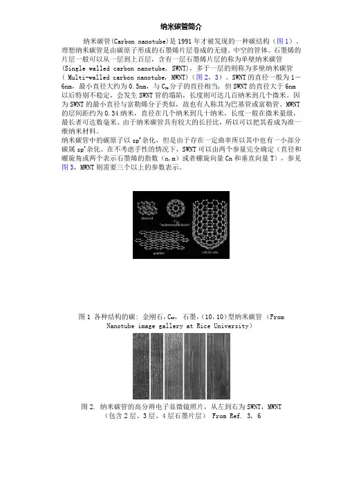
纳米碳管简介纳米碳管(Carbon nanotube)是1991年才被发现的一种碳结构(图1)。
理想纳米碳管是由碳原子形成的石墨烯片层卷成的无缝、中空的管体。
石墨烯的片层一般可以从一层到上百层,含有一层石墨烯片层的称为单壁纳米碳管(Single walled carbon nanotube, SWNT),多于一层的则称为多壁纳米碳管( Multi-walled carbon nanotube, MWNT)(图2,3)。
SWNT的直径一般为1-6nm,最小直径大约为0.5nm,与C36分子的直径相当, 但SWNT的直径大于6nm 以后特别不稳定,会发生SWNT管的塌陷,长度则可达几百纳米到几个微米。
因为SWNT的最小直径与富勒烯分子类似,故也有人称其为巴基管或富勒管。
MWNT 的层间距约为0.34纳米,直径在几个纳米到几十纳米,长度一般在微米量级,最长者可达数毫米。
由于纳米碳管具有较大的长径比,所以可以把其看成为准一维纳米材料。
纳米碳管中的碳原子以sp2杂化,但是由于存在一定曲率所以其中也有一小部分碳属sp3杂化。
在不考虑手性的情况下,SWNT可以由两个参量完全确定(直径和螺旋角或两个表示石墨烯的指数(n,m)或者螺旋向量Cn和垂直向量T〕,参见图3,MWNT则需要三个以上的参数表示。
图1 各种结构的碳: 金刚石,C60,石墨,(10,10)型纳米碳管(From Nanotube image gallery at Rice University)图2. 纳米碳管的高分辨电子显微镜照片,从左到右为SWNT,MWNT(包含2层、3层、4层石墨片层) From Ref. 3, 6图3 从石墨烯片层构造纳米碳管示意图历史纳米碳管研究是富勒烯(C 60,C 70...)继续,1991年,理论预计纳米碳管具有许多的奇特电学性能[1][2],几乎同时NEC 公司S Iijima 在高分辨电子显微镜下观察采用电弧法制备的富勒烯中发现了一种管状结构,经过研究表明它们是同轴多层富勒管,被称为多壁纳米碳管[3],随后NEC 公司的TW Ebbesen 和PM Ajayan 找到大量制备MWNT 方法[4]。
碳纳米管(CNTs)班级:材料化学班姓名:唐建学号:20110513427摘要:1991年日本NEC公司的饭岛纯雄(Sumio Iijima)首次利用电子显微镜观察到中空碳纤维,直径一般在几纳米到几十个纳米之间,长度为数微米,甚至毫米,称为“碳纳米管”。
从此便引发了碳纳米管研究的热潮和近十几年来碳纳米管科学和技术的飞速发展。
本文主要分为两部分:1、对纳米材料及碳纳米管的相关知识进行介绍2、于应用层次,讨论纳米材料及碳纳米管的应用前景关键字:纳米材料概述碳纳米管热点及应用1、引言生物科学技术、信息科学技术、纳米科学技术是下一世纪内科学技术发展的主流。
生物科学技术中对基因的认识,产生了转基因生物技术,可以治疗顽症,也可以创造出自然界不存在的生物;信息科学技术使人们可以坐在家中便知天下大事,因特网几乎可以改变人们的生活方式。
而纳米科学技术作为二十一世纪的主导产业,又将给人们带来怎样天翻地覆的改变呢?……2、理论知识2.1 纳米材料概述纳米材料:指晶粒尺寸为纳米级(10-9米)的超细材料。
从材料的结构单元层次来说,它处于宏观物质和微观原子、分子之间的介观领域。
在纳米材料中,界面原子占极大比例,而且原子排列互不相同,界面周围的晶格结构互不相关,从而构成与晶态、非晶态均不同的一种新的结构状态。
纳米科学技术:研究在千万分之一米(10-8)到亿分之一米(10-9米)内,原子、分子和其它类型物质的运动和变化的学问;同时在这一尺度范围内对原子、分子进行操纵和加工又被称为纳米技术。
2.2 纳米材料的特性2.2.1纳米材料的体积效应体积效应中的典型例子是久保理论。
其是针对金属纳米粒子费米面附近电子能级状态分布而提出的。
该理论把金属纳米粒子靠近费米面附近的电子状态看作是受尺寸限制的简并电子态,并进一步假设它们的能级为准粒子态的不连续能级,并认为相邻电子能级间距δ和金属纳米粒子的直径d的关系为:δ=4EF/3N ∞V-1 ∞1/d3(其中N为一个金属纳米粒子的总导电电子数,V为纳米粒子的体积;EF为费米能级)。
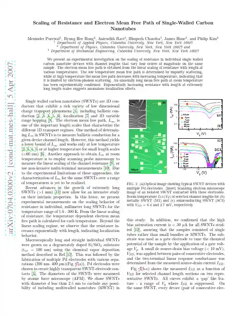
a r X i v :0704.0300v 2 [c o n d -m a t .m e s -h a l l ] 5 A p r 2007Scaling of Resistance and Electron Mean Free Path of Single-Walled CarbonNanotubesMeninder Purewal 1,Byung Hee Hong 2,Anirudhh Ravi 2,Bhupesh Chandra 3,James Hone 3,and Philip Kim 21Department of Applied Physics,Columbia University,New York,New York 100272Department of Physics,Columbia University,New York,New York 10027and3Department of Mechanical Engineering,Columbia University,New York,New York 10027We present an experimental investigation on the scaling of resistance in individual single walled carbon nanotube devices with channel lengths that vary four orders of magnitude on the same sample.The electron mean free path is obtained from the linear scaling of resistance with length at various temperatures.The low temperature mean free path is determined by impurity scattering,while at high temperature the mean free path decreases with increasing temperature,indicating that it is limited by electron-phonon scattering.An unusually long mean free path at room temperature has been experimentally confirmed.Exponentially increasing resistance with length at extremely long length scales suggests anomalous localization effects.Single walled carbon nanotubes (SWNTs)are 1D con-ductors that exhibit a rich variety of low dimensional charge transport phenomena [1],including ballistic con-duction [2,3,4,5,6],localization [7]and 1D variable range hopping [8].The electron mean free path,L m ,is one of the important length scales that characterize the different 1D transport regimes.One method of determin-ing L m in SWNTs is to measure ballistic conduction for a given device channel length.However,this method yields a lower bound of L m ,and works only at low temperature [2,3,4,5]or at higher temperature for small length scales (<60nm)[6].Another approach to obtain L m at room temperature is to employ scanning probe microscopy to measure the linear scaling of the channel resistance [9],or use non-invasive multi-terminal measurements [10].Due to the experimental limitations of these approaches,the characterization of L m for the same SWNTs over a range of temperatures is yet to be realized.Recent advances in the growth of extremely long SWNTs (>1mm)[11]now allow for an intensive study on their intrinsic properties.In this letter,we present experimental measurements on the scaling behavior of resistance in individual,millimeter long SWNTs for the temperature range of 1.6-300K.From the linear scaling of resistance,the temperature dependent electron mean free path is calculated for each temperature.Beyond the linear scaling regime,we observe that the resistance in-creases exponentially with length,indicating localization behavior.Macroscopically long and straight individual SWNTs were grown on a degenerately doped Si/SiO 2substrate (t ox =500nm)using the chemical vapor deposition method described in Ref.[11].This was followed by the fabrication of multiple Pd electrodes with various sepa-rations (200nm-400µm)(Fig.1(a)).Pd electrodes were chosen to create highly transparent SWNT-electrode con-tacts [4].The diameters of the SWNTs were measured by atomic force microscope (AFM).We chose SWNTs with diameter d less than 2.5nm to exclude any possi-bility of including multiwalled nanotubes (MWNT)in500ȝm 20ȝm(a)FIG.1:(a)Optical image showing typical SWNT devices with multiple Pd electrodes.(Inset)Scanning electron microscope image of an isolated SWNT contacted with these electrodes.Room temperature I SD (V g )of selected channel lengths for (b)metallic SWNT (M1)and (c)semiconducting SWNT (SC3)with V SD =6.4and 2.7mV,respectively.this study.In addition,we confirmed that the high bias saturation current is <30µA for all SWNTs stud-ied [12],assuring that the samples consisted of single tubes rather than small bundles or MWNTs.The sub-strate was used as a gate electrode to tune the chemical potential of the sample by the application of a gate volt-age V g .A small dc source-drain bias voltage (<10mV),V SD ,was applied between pairs of consecutive electrodes,and the two-terminal linear response conductance was determined from the measured source-drain current I SD .Fig.1(b-c)shows the measured I SD as a function of V SD for selected channel length sections on two repre-sentative SWNTs.All curves exhibit a ‘gap’like fea-ture -a range of V g where I SD is suppressed.On the same SWNT,every device (pair of consecutive elec-2trodes)shows a similar I SD(V g)up to a length-dependent multiplicative factor,once we align the centers of the gap region for each curve.The similarity of the I SD(V g) behavior in different sections for each SWNT sample indicates that the corresponding‘gap’features are de-rived from the intrinsic electronic structure of the SWNT rather than the effects of random local variation.We use the qualitatively different I SD(V g)behaviors of different SWNTs to categorize them as metallic(M-NT) orsemiconducting nanotubes(S-NT).Typical S-NTs(Fig.1(c))exhibit an offcurrent region I SD<10−10A when the Fermi energy E F lies n the energy gap[13,14].On the other hand,a weaker suppression of I SD(V g)is observed in the‘small gap’region in M-NTs(Fig.1(b)).The‘small gap’in M-NTs has been attributed to thecurvature-induced energy gap E g<100meV[15],which is distinguished from the S-NT energy gap,which scaleswith diameter as E g∼1/d(nm)[1].Among the11 SWNTs we studied in this letter,we found4M-NTs and7S-NTs.Each of these SWNTs exhibit a gap cen-tered at V g>0,indicating their p-doped nature.At large negative gate voltage(V g<−20V),E F lies welloutside of the gap region and I SD(V g)saturates to I satSD ,whose value depends only on the applied V SD and chan-nel length L of the SWNT section.The two-terminal resistance of the SWNT section is then obtained fromR(L)=V SD/I satSD .We note that four-terminal resistancemeasurements are possible for each section by utilizing the available multiple electrode configuration.However, in our experiment,the four terminal measurements yield essentially similar results to the two terminal R(L),which prevents separation of the‘contact’resistance contribu-tion from R(L).Such inseparable contact resistance be-tween SWNT-metal electrodes was reported to be caused by the invasiveness of metal contacts[16].We designed many pairs of electrodes with different L on each SWNT so that the scaling of R(L)can be studied for a specific sample at a given temperature T.Fig.2(a) show R(L)of a representative SWNT measured in the temperature range of1.6-300K and with an L range of 200nm-50µm.In these ranges,R(L)increases linearly and appears to converge to afinite value for small L(in-set to Fig.2(a)).We found that this scaling behavior can be described well by a simple linear dependence with an offset:R(L)=ρL+R c,whereρand R c are interpreted as the1D resistivity and contact resistance,respectively. The solid lines in Fig.2(a)are the two parameter line fits of the data points at a given T value.From these fits,R c(T)andρ(T)are obtained as shown in Fig.2(b) and Fig.2(c),respectively.For this sample,R c remains fairly constant at∼8kΩandρ(T)exhibits typical metal-lic behavior,i.e.it decreases with T and saturates to a valueρsat at low temperatures.Similar scaling behavior of R(L)is observed in other SWNTs,from which both R c andρ(T)are extracted within the linear scaling regime. Table I summarizes d,R c,andρsat for the4M-NTs FIG.2:(a)(Inset)R(L)for sample M1at select temperatures ranging from1.6-300K.(Main)A log-log plot highlights the behaviors at different lengths scaling3orders of magnitude. From the linearfits(solid lines)of these data points,we ob-tain the1D resistivity(b)and the contact resistance(c)at different temperatures.The dashed line in(c)represents R Q. and7S-NTs considered in this study.To understand thescaling of R(L)in Fig.2,we begin with the two-terminal Landauer-Buttiker formula applied to SWNTs[9].If weconsider4low-energy channels in the SWNT,2each forspin and band degeneracy,then the scaling of resistance is given by R(L)=(h/4e2)(L/L m+1)+R nc,where eand h are electron charge and Plank constant and L m and R nc are the electron mean free path and the non-transparent contact resistance,respectively.Note thatwe separate out the contribution of R nc from the total contact resistance R c,so that the contact resistance be-comes the quantum resistance R Q=h/4e2when the con-tacts become fully transparent.From the experimentally obtainedρ(T)and R c,we can deduce L m=R Q/ρ(T)and R nc=R c−R Q for each of our SWNT samples.In particular,we note that R nc<∼R Q for the majority of our samples,suggesting that the barrier at the contactsis very thin and adds only a negligible contribution when L becomes substantially large.We now discuss the temperature dependent behaviorof the mean free path.Fig.3is the central result ofthis letter,showing L m(T)of the SWNTs listed in Ta-ble I.Overall,L m(T)exhibits different behaviors in two regimes separated by T cr:(i)the high tempera-ture regime(T>T cr)where L m∼T−1(dashed line in Fig.3),which indicates that inelastic scattering be-3 TABLE I:Device characteristics for SWNTs used in this study.The character M(SC)is designated for metallic(semiconduct-ing)SWNTs.M2M4SC2SC4SC62.0±.21.7±.61.6±.41.9±.42.2±.22.2±.27.9±.88.3±2.510.2±4.510.4±.925.4±4.221.8±140.76±.020.93±.012.95±.054.64±.018.13±.3116.3±.138.56±.237.07±.082.24±.041.40±.010.80±.030.40±.014strong sample dependent behavior,generally we found L c>>L m in all temperature ranges,with the tempera-ture dependence exhibiting a trend of increasing L c with increasing T(upper insets to Fig.4).This observed be-havior of L c(T)excludes the quantum interference re-lated to strong localization effects such as Anderson Lo-calization[7]from the possible scenarios.In particular,inthe high temperature regime(T>T cr),the phase coher-ence length Lφis limited by the phase-breaking electron-phonon scattering,and thus Lφ∼L m<<L c,inviting further study to elucidate the observed localization be-havior beyond the strong localization limit[22,23].In conclusion,we determine the length dependent re-sistance for SWNTs with channel lengths ranged200nm -400µm.From the scaling behavior we evaluate the electron mean free path and localization length of the SWNT for a range of temperatures.While the low tem-perature mean free path is determined by the impurity scattering,an unusually long mean free path is demon-strated at room temperature,even with the dominant electron-phonon scattering.We thank I.Aleiner, B.Altshuler,and P.Jarillo-Herrero for helpful discussions.This work is supported by the NSF NIRT(ECS0507111),CAREER(DMR-0349232),NSEC(CHE-0117752),and the New York State Office of Science,Technology,and Academic Re-search(NYSTAR).[1]R.Saito,G.Dresselhaus,and M.S.Dresselhaus,PhysicalProperties of Carbon Nanotubes(Imperial College Press, London1998).[2]J.Kong,E.Yenilmez,T.W.Tombler,W.Kim,H.Dai,ughlin,L.Liu,C.S.Jayanthi,and S.Y.Wu,Phys.Rev.Lett.87,106801(2001).[3]W.Liang,M.Bockrath, D.Bozovic,J.H.Hafner,M.Tinkham,and H.Park,Nature411,665(2001).[4]D.Mann,A.Javey,J.Kong,Q.Wang,and H.Dai,NanoLett.3,1541(2003).[5]A.Javey,J.Guo,Q.Wang,M.Lundstrom and H.Dai,Nature,424,654(2003).[6]A.Javey,J.Guo,M.Paulsson,Q.Wang,D.Mann,M.Lundstrom,and H.Dai,Phys.Rev.Lett.92,106804 (2004).[7]C.Gomez-Navarro,P.J.de Pablo,J.Gomez-Herrero,B.Biel, F.J.Garcia-Vidal, A.Rubio and F.Flores,Nat.Mater.4,534(2005).[8]B.Gao,D.C.Glattli,B.Placais and A.Bachtold,Phys.Rev.B74,085410(2006).[9]J.Park,S.Rosenblatt,Y.Yaish,V.Sazonova,-tunel,S.Braig,T.A.Arias,P.W.Brouwer and P.L.McEuen,Nano Lett.4,517(2004).[10]B.Gao,Y.F.Chen,M.S.Fuhrer,D.C.Glattli,and A.Bachtold,Phys.Rev.Lett.95,196802(2005).[11]B.H.Hong,J.Y.Lee,T.Beetz,Y.Zhu,P.Kim,and K.S.Kim,J.Am.Chem.Soc.127,15336(2005).[12]Z.Yao,C.L.Kane,and C.Dekker,Phys.Rev.Lett.84,2941(2000).[13]S.J.Tans,A.R.M.Verschueren,and C.Dekker,Nature393,49(1998).[14]J.Appenzeller,J.Knoch,V.Derycke,R.Martel,S.Windand Ph.Avouris,Phys.Rev.Lett.89,126801(2002). [15]C.Zhou,J.Kong,and H.Dai,Phys.Rev.Lett.84,5604(2000).[16]A.Bezryadin,A.R.M.Verschueren,S.J.Tans,and C.Dekker,Phys.Rev.Lett.80,4036(1998).[17]V.Perebeinos,J.Tersoff,and Ph.Avouris,Phys.Rev.Lett.94,086802(2005).[18]X.Zhou,J.Park,S.Huang,J.Liu,and P.L.McEuen,Phys.Rev.Lett.95,146805(2005).[19]A.Bachtold,M.S.Fuhrer,S.Plyasunov,M.Forero,E.H.Anderson,A.Zettl,and P.L.McEuen,Phys.Rev.Lett.84,6082(2000).[20]T.Ando and T.Nakanishi,Jpn.J.Appl.Phys.67,1704(1998).[21]P.L.McEuen,M.Bockrath,D.H.Cobden,Y.G.Yoon,and S.G.Louie,Phys.Rev.Lett.83,5098(1999). [22]F.Triozon,S.Roche,A.Rubio,and D.Mayou,Phys.Rev.B69,121410(R)(2004).[23]R.Avriller,til,F.Triozon,X.Balse,and S.Roche,Phys.Rev.B74,121406(R)(2006).。
1 引言纳米材料是纳米技术的基础,而碳纳米管又可称为纳米材料之王。
碳纳米材料在纳米材料技术开发中举足轻重,它将影响到国民经济的各个领域。
碳纳米管的发现是碳团簇领域的又一重大科研成果,本文探讨了碳纳米管的结构、特性、活化方法,评述了这种纳米尺寸的新型碳材料在电化学器件、氢气存储、场发射装置、碳纳米管场效应晶体管、催化剂载体、碳纳米管修饰电极领域的应用价值,展望了碳纳米管的介入对全球性物理、化学及材料等学科界所带来的美好前景。
在1991年日本NEC公司基础研究实验室的电子显微镜专家饭岛(Iijima)在高分辨透射电子显微镜下检验石墨电弧设备中产生的球状碳分子时,意外发现了由管状的同轴纳米管组成的碳分子,这就是现在被称作的“Carbon nanotube”,即碳纳米管,又名巴基管。
1993年。
S.Iijima等和DS。
Bethune等同时报道了采用电弧法,在石墨电极中添加一定的催化剂,可以得到仅仅具有一层管壁的碳纳米管,即单壁碳纳米管产物。
1997年,AC.Dillon等报道了单壁碳纳米管的中空管可储存和稳定氢分子,引起广泛的关注。
相关的实验研究和理论计算也相继展开。
初步结果表明:碳纳米管自身重量轻,具有中空的结构,可以作为储存氢气的优良容器,储存的氢气密度甚至比液态或固态氢气的密度还高。
适当加热,氢气就可以慢慢释放出来。
研究人员正在试图用碳纳米管制作轻便的可携带式的储氢容器。
据推测,单壁碳纳米管的储氢量可达10%(质量比)。
此外,碳纳米管还可以用来储存甲烷等其他气体。
利用碳纳米管的性质可以制作出很多性能优异的复合材料。
例如用碳纳米管材料增强的塑料力学性能优良、导电性好、耐腐蚀、屏蔽无线电波。
使用水泥做基体的碳纳米管复合材料耐冲击性好、防静电、耐磨损、稳定性高,不易对环境造成影响。
碳纳米管增强陶瓷复合材料强度高,抗冲击性能好。
碳纳米管上由于存在五元环的缺陷,增强了反应活性,在高温和其他物质存在的条件下,碳纳米管容易在端面处打开,形成一个管子,极易被金属浸润、和金属形成金属基复合材料。
单壁碳纳米管拉曼蓝移单壁碳纳米管(Single-walled carbon nanotubes,SWCNTs)是一种由单层碳原子构成的管状结构,具有很多独特的物理和化学性质。
SWCNTs的直径通常在1-2纳米之间,长度可以达到数百微米,具有很大的特殊表面积和高机械强度。
SWCNTs的应用领域非常广泛,包括材料科学、化学、生物医学、磁性材料、电子学、光学和能源等。
SWCNTs常常受到拉曼光谱的研究。
拉曼散射是一种非常有用的工具,可以用来研究物质的结构和相互作用,其中最重要的是非共价键的振动模式。
SWCNTs被认为是拉曼散射研究的理想对象之一,因为它们的非共价键振动模式可以被非常清晰地观察到。
当SWCNTs吸收光子时,非共价键振动模式(例如G带、D带和2D带)会发生蓝移或红移,这取决于管子直径、构象和环境。
SWCNTs的非共价键振动模式中G带是最常见的振动模式,它由管子中的全息振动形成。
D带则是由通常来自管中的特殊结构造成。
2D带如同G带一样,由全息振动形成,但与G带有明显的不同,在波数上一般会比G带高。
因此,通过测量不同的非共价键振动模式的拉曼光谱特征,可以得到SWCNTs的长度、直径和构象等信息。
同时,拉曼光谱也可以用来监测SWCNTs的应力和环境变化,并且可用于研究SWCNTs在材料科学和生物医学领域的应用。
SWCNTs的拉曼散射是非常有趣的,因为它们的结构和相互作用具有独特的特征。
在SWCNTs中,由于非共价键振动模式的存在,原子之间的相互作用会发生变化。
这种相互作用通常是短程的,它可以引起SWCNTs的结构变化,进而影响SWCNTs的光学性质。
SWCNTs的环境和外部应力会影响振动模式和相互作用,从而影响拉曼散射的表现形式。
因此,通过拉曼光谱技术可以获得SWCNTs的相关信息,特别是SWCNTs的电子能带结构、化学结构、晶格结构、应力分布和表面修饰等等。
SWCNTs的拉曼散射被广泛应用于各种领域。
ocsial单壁碳纳米管产能单壁碳纳米管(Single-walled carbon nanotubes,SWCNTs)是由以碳为主要成分的原子构成的纳米管状结构,具有很高的强度和导电性能,被广泛应用于多个领域。
本文将重点讨论SWCNTs的产能及其相关问题。
SWCNTs的产能受到多个因素的影响。
首要因素是生产方法的选择。
目前,SWCNTs的制备方法主要包括电弧放电法、化学气相沉积法和溶液法等。
其中,电弧放电法是最早被发现的制备SWCNTs的方法,虽然产量较高,但产品纯度较低。
而化学气相沉积法则能获得较高纯度的SWCNTs,但产量较低。
溶液法是一种相对简单且可大规模生产的方法,但需要进一步提高产能和纯度。
SWCNTs的产能还受到原材料的限制。
目前主要使用的原料是石墨粉末,但其制备成本较高且资源有限。
因此,寻找更多的原料来源以及开发新的制备方法将有助于提高SWCNTs的产能。
SWCNTs的产能还受到设备和工艺的限制。
现有的生产设备和工艺在提高产能和纯度方面仍存在挑战。
例如,电弧放电法需要改进电极材料和电弧放电条件,化学气相沉积法需要优化催化剂和沉积条件,溶液法需要改进分离和纯化方法。
同时,开发高效的工艺流程和提高设备的稳定性也是提高SWCNTs产能的关键。
SWCNTs的产能还受到市场需求的影响。
目前,SWCNTs在电子、储能、催化、生物医学等领域都有广泛的应用前景。
随着这些领域的不断发展和需求的增加,SWCNTs的产能也将逐步提高。
SWCNTs的产能受到多个因素的影响,包括生产方法、原材料、设备和工艺以及市场需求等。
通过不断改进和创新,提高SWCNTs的产能将有助于推动其在各个领域的应用和发展。

碳纳米管的分类英语Carbon nanotubes are fascinating materials that come in various types. You know, there's single-walled nanotubes, which are like super-thin tubes made of a single layer of carbon atoms. They're strong and lightweight, making them great for nanoelectronics and composites.On the other hand, multi-walled nanotubes have multiple layers of carbon atoms, like a Russian nesting doll. These are more stable and can handle higher temperatures, whichis why they're often used in aerospace applications.Functionally, you've got chiral nanotubes, which have a spiral shape. They're unique in their electrical properties and can be used in sensors or as conductors in specialized electronics.But if you're looking for nanotubes that are arrangedin a specific way, there are arrayed nanotubes. Think of them like a forest of carbon nanotubes standing upright.These arrays have excellent thermal conductivity and are used in heat dissipation systems.And let's not forget about the hybrid nanotubes. These are a combination of different types, like single-walled nanotubes wrapped in another material for added properties. Hybrids are the future of carbon nanotechnology, offering endless possibilities for customization and functionality.。
碳纳米管中的大π键-概述说明以及解释1.引言1.1 概述碳纳米管是一种具有特殊结构和优异性能的纳米材料,在纳米科技领域引起了广泛的关注和研究。
其独特的性质主要源于构成碳纳米管的碳原子与相邻碳原子之间形成的特殊键,即π键。
π键是一种共轭键,具有高度的共轭性和稳定性,对于碳纳米管的形成和性质具有重要影响。
本文将重点探讨碳纳米管中的大π键,大π键是指连接两个相邻的碳原子的共轭键的存在形式。
在碳纳米管中,大π键的形成机制引发了广泛的讨论与研究。
同时,我们将探讨大π键对碳纳米管性质的影响以及其在各个领域中的应用前景。
此外,本文还将对碳纳米管中大π键的研究未来发展方向进行展望。
通过深入了解碳纳米管中的大π键,我们可以更好地理解世界各地科学家关于碳纳米管研究的努力和成果。
同时,对于探索碳纳米管的新的应用领域和进一步提高其性能也具有重要意义。
希望本文的研究和总结可以为相关科学家提供有关碳纳米管中的大π键的全面知识和启示,进一步促进碳纳米管领域的发展和应用。
1.2文章结构文章结构部分的内容:本文主要分为引言、正文和结论三部分。
引言部分主要介绍本文的研究背景和意义。
首先概述了碳纳米管的基本概念和特点,引出了本文的研究对象。
接着,简要介绍了本文的结构,先分析碳纳米管的基本结构,然后详细说明碳纳米管中的π键的定义与特点,最后探讨碳纳米管中大π键的形成机制。
最后,阐述了本文的目的,为读者提供本文的研究重点和目标。
正文部分将从碳纳米管的基本结构、碳纳米管中的π键的定义与特点以及碳纳米管中大π键的形成机制三个方面进行论述。
首先,详细介绍碳纳米管的基本结构,包括其形状、尺寸等特征。
然后,解释碳纳米管中π键的含义、特性和与其它键的区别。
接着,探讨碳纳米管中大π键的形成机制,包括分子轨道理论、共轭体系等方面的讨论,以及相关的实验结果和研究方法。
结论部分总结了本文的研究结果和发现。
首先,分析了碳纳米管中大π键对其性质的影响,包括导电性、稳定性等方面的讨论。
单壁碳纳米管透明导电薄膜单壁碳纳米管(Single-walled carbon nanotube,SWCNT)是一种具有优异电学、光学和力学性能的纳米材料。
将单壁碳纳米管用于制备透明导电薄膜,具有重量轻、透明度高、机械强度好等优点。
这种薄膜可用于各种需要导电和透明的应用场合,如触摸屏、显示器、太阳能电池等。
下面是大致的生产过程:1.制备单壁碳纳米管:首先需要制备高纯度的单壁碳纳米管。
目前制备单壁碳纳米管的方法主要有电弧放电法、激光蒸发法和化学气相沉积法等。
2.制备透明导电薄膜:将制备好的单壁碳纳米管分散在溶剂中,形成均匀的分散液。
然后通过涂布、喷涂或旋涂等方法将分散液均匀涂布在基材上,形成一层薄膜。
最后经过高温处理,使碳纳米管在基材上形成连续的网络结构,从而提高薄膜的导电性和透明度。
单壁碳纳米管透明导电薄膜的应用:1.透明电极:由于单壁碳纳米管透明导电薄膜具有高透明度和良好的导电性能,因此可以作为透明电极的候选材料。
例如,可以用于制备透明触控屏、透明发光器件等。
2.柔性电子器件:由于单壁碳纳米管透明导电薄膜具有良好的柔性和可延展性,因此可以用于制备柔性电子器件,如柔性显示器、柔性太阳能电池等。
3.传感器:单壁碳纳米管透明导电薄膜可以用于制备气体传感器、湿度传感器等,由于其良好的导电性能和灵敏度,可以实现对气体和湿度的快速响应和检测。
4.防雾防霜涂层:由于单壁碳纳米管透明导电薄膜具有优异的导热性能和电学性能,因此可以用于制备防雾防霜涂层,提高光学器件的透过率和清晰度。
5.电磁屏蔽:单壁碳纳米管透明导电薄膜具有良好的电磁屏蔽效果,可以用于制备电磁屏蔽材料和吸波材料等,有效降低电磁辐射对人体的危害。
6.散热材料:由于单壁碳纳米管透明导电薄膜具有优异的导热性能,因此可以用于制备散热材料,解决电子设备散热问题。
以上内容仅供参考,建议咨询专业人士获取更准确的信息。
单壁碳纳米管的制备、提纯、分离及其在纳电子器件中的应用The Preparation, Purification, Dispersion and Application in Nanoscale Electronic Devices of Single-walled Carbon Nanotubes电子学系 99级赵晓雪摘要本文简要介绍了单壁碳纳米管的电弧法制备和提纯。
为使其能够应用于纳电子器件中,对提纯后的样品进行了超声波分离。
选用了不同的溶剂、浓度配比和超声时间。
初步尝试出乙醇和异丙醇为较好的溶剂。
样品纯度对分离的效果有直接的影响。
AbstractSingle-walled carbon nanotubes (SWTs) are prepared by the standard arc-discharge method and then purified. In order to pave the way for the application of SWTs in nanoscale field-effect transistor (FET), we disperse the tubes in several different solvents ultrasonically to attainindividual tubes. The best results were obtained using ethanol and isopropanol. The effect of dispersion depends remarkably on the sample purity.一、碳纳米管的制备㈠、碳纳米管的种类理想的碳纳米管(T)是由碳原子形成的石墨片层卷成的无缝、中空的管体,可包含一层到上百层石墨层。
只有一层石墨片层的称为单壁碳纳米管(Single- walled carbon nanotube,SWNT or SWT),含有一层以上石墨片层的则称为多壁碳纳米管( Multi-walled carbon nanotube,MWNT or MWT)。
多孔硅包裹的单壁碳纳米管作为药物载体用于癌症联合治疗刘晶晶,汪超,刘庄*苏州大学功能纳米与软物质研究院,江苏省苏州市工业园区仁爱路199号,215123*Email: zliu@单壁碳纳米管在光热治疗和药物装载领域的应用已经被广泛研究。
在这个工作中,我们选择具有生物相容性的介孔二氧化硅来包裹单壁碳纳米管,并在二氧化硅表面修饰生物相容性的高分子聚乙二醇(PEG),而不破坏单壁碳纳米管本身的性质(如拉曼信号和近红外吸收)。
然后通过介孔二氧化硅表面吸附和疏水作用装载化疗药物如阿霉素,发现具有超高的装载效率(~ 500%)。
这种多孔硅包裹的单壁碳纳米管作为药物载体,具pH响应的性质,同时在近红外激光照射下具有热促进释放的功能。
通过实验表明这种复合载体在细胞和活体水平上具有很好的光热治疗和化疗治疗效果,并且在较低的功率和剂量下实现了很好的联合治疗效果,有可能在纳米生物医学中得到进一步的应用。
关键词:单壁碳纳米管;介孔二氧化硅;药物载体;联合治疗Mesoporous silica coated single-walled carbon nanotube served as drug carrier used for cancer combination therapyJingjing Liu, Chao Wang, Zhuang Liu(Z. Liu)*Functional Nano & Soft Materials Laboratory (FUNSOM) and Jiangsu Key Laboratory for Carbon-Based Functional Materials & Devices,SoochowUniversity,Suzhou, Jiangsu 215123Single-walled carbon nanotube (SWNT) has shown great potential applications in drug delivery system and photothermal therapy. Herein, SWNT was coated by the mesoporous silica shell duo to its well bio-compatibility. Then PEG was used to further modify the material to improve the water solubility without disrupting the structure of SWNT (such as Raman signal and absorption of NIR). Furthermore, anti-cancer drugs such as doxorubicin can be loaded into the nanocomposite through hydrophobic interactions and adsorption, with high loading content (more than 500%). In this work, this mesoporous silica coated SWNT showed pH-responsive and heat-stimulative properties. In addition, this composited platform was proved to be effective in photothermal therapy and chemotherapy in vitro and in vivo. What’t more, a great synergestic therapeutic effect was achieved under the much lower dosage and power intensity of NIR laser, so this functionalized nanocarrier would play a role in the nano-biomedicine in the future.。
碳纳米管场效应晶体管开关原理1.引言碳纳米管场效应晶体管(Ca rb on Na no tub e Fi el d-E f fe ct Tr an si st or,C NF ET)是一种新型的纳米电子器件,具有优异的电子性能和潜在的应用前景。
本文将介绍碳纳米管场效应晶体管开关的原理及其工作机制。
2.碳纳米管简介碳纳米管是由碳原子构成的纳米尺寸管状结构,具有高强度、优异的导电性和热导性能。
碳纳米管的直径通常在纳米级别,长度可达到数微米或更长。
碳纳米管可分为单壁碳纳米管(S i ng le-W a ll ed Ca rb on Na not u be,S WC NT)和多壁碳纳米管(Mu lt i-W a ll ed Ca rb on Na not u be,M WC NT)两种形式。
3.原理介绍碳纳米管场效应晶体管是利用碳纳米管在电场作用下的电荷运输性质来实现电子的控制和开关。
其主要元件结构包括源极(So ur ce)、漏极(D ra in)、栅极(G a te)和碳纳米管通道。
3.1漏极和源极漏极和源极是碳纳米管场效应晶体管的电流引脚,用于控制电子的流动。
当栅极施加一定电压后,栅极与源极之间建立电场,使得碳纳米管通道中的电子发生运动。
3.2栅极栅极是用于控制碳纳米管通道导电性的部分。
当栅极施加电压时,会产生电场,而碳纳米管通道中的电子受到电场的作用而发生移动。
3.3碳纳米管通道碳纳米管通道是整个晶体管的核心部分,它连接源极和漏极,是电子流动的通道。
碳纳米管通道的导电性质可以通过施加栅极电压来控制,实现对电流的调控。
4.工作原理碳纳米管场效应晶体管的工作原理主要通过栅极电压控制通道中的电子运动。
具体工作步骤如下:1.初始状态下,碳纳米管通道中没有电子流动,栅极电压为低电平。
2.当栅极施加一定电压时,栅极与源极之间建立电场,使得碳纳米管通道中的电子发生运动。
3.当栅极电压为高电平时,电子受到栅极电场的吸引,从源极流向漏极,形成漏电流。
单壁碳纳米管
单壁碳纳米管(single-wall carbon nanotubes,简称 SWCNTs)是1997年由斯坦福
大学实验室发现的一种新型碳材料,它具有直径介于纳米毫米量级的结构、高比表面积、
体积极小、有机化学活性及很好的电导能力,深受科学家的青睐。
单壁碳纳米管以碳原子以六角环结构形成一条管道,长度可以从几个至几十个纳米米,极微小的直径可以用双精度锰原子比喻(约等于1.3千分之一毫米),而他们周围以一层
自由电子形成单壁结构,该结构可通过气体直接生长——弥散解离,从而构成几个十亿分
之一厘米厚度的非常薄的壁。
单壁碳纳米管的主要物理性能在其软内芯的单空间结构内发
挥着,这也导致了该材料拥有很好的电子传输性和电导能力,高的崩溃抵抗能力、良好的
化学稳定性、良好的机械性能及难以穿透的谐振光栅效应,从而使其成为科学家研究的热
点方向之一。
目前,单壁碳纳米管在电子材料领域具有广泛的应用,如作为超级电容器的电极材料,纳米晶体管和柔性显示器等。
另外,单壁碳纳米管作为光学元件加以利用,正被用于集成
光学器件。
在医学领域,单壁碳纳米管更是使用广泛,它可以作为抗癌药物递送系统、靶
向的生物标记物、磁共振成像剂等。
总之,单壁碳纳米管的超高性能和体积极小的特点,使它成为许多无数创新应用的重
要原料之一,后续研究及利用会更加发展广泛,期待其在电子,光电,医学等工程领域得
到更多的发展与实践应用,从而带动近年来被普济科学的发展。
喷涂法制备单壁碳纳米管柔性透明导电薄膜及其性能研究胡晓燕;李家权;陈蓓蓓;耿宏章【摘要】The single-walled carbon nanotubes ( SWCNTs) were dispersed in deionized water with sodium dode-cyl benzene sulfonate as dispersant by bath sonication method. Flexible transparent conducting films ( TCFs) were fabricated on poly( ethylene terephthalate) substrate by a spray coating method using the SWCNT solution. We ana-lyzed the TCFs by transmittance,sheet resistance,flexibility and scanning electron microscopy. The fabricated TCFs have good performance with highflexibility,uniformity,high transparency and low sheet resistance. It has potential applications in many fields such as flexible flat paneldisplay,touch screen and organic light-emitting diodes.%采用喷涂的方法将以十二烷基苯磺酸钠为分散剂分散在去离子水中的单壁碳纳米管喷涂到聚对苯二甲酸乙二酯基底上制备了柔性透明导电薄膜,研究了薄膜透光率与面电阻的关系、表面形貌及其弯曲状态的面电阻,结果表明这种透明导电薄膜具有高柔韧性、高透光度和低面电阻等优点,在柔性显示器、触摸屏、有机发光器件等方面有广阔的应用前景.【期刊名称】《合成材料老化与应用》【年(卷),期】2017(046)005【总页数】6页(P51-56)【关键词】单壁碳纳米管;柔性透明导电薄膜;喷涂;面电阻【作者】胡晓燕;李家权;陈蓓蓓;耿宏章【作者单位】贵州分析测试研究院,贵州贵阳550001;;贵州分析测试研究院,贵州贵阳550001;天津工业大学材料科学与工程学院,天津300387【正文语种】中文【中图分类】TQ127.1;O439单壁碳纳米管(Single-walled carbon nanotubes,SWCNTs)是由单层石墨层卷曲构成的管状结构,其直径小、缺陷小,具有较高的均匀一致性[1]。
Single-Walled Carbon Nanotube ElectronicsPaul L.McEuen,Michael S.Fuhrer,and Hongkun Park Abstract—Single-walled carbon nanotubes(SWNTs)haveemerged as a very promising new class of electronic materials.The fabrication and electronic properties of devices based onindividual SWNTs are reviewed.Both metallic and semicon-ducting SWNTs are found to possess electrical characteristicsthat compare favorably to the best electronic materials available.Manufacturability issues,however,remain a major challenge.Index Terms—Field-effect transistors(FETs),interconnections,nanotechnology,nanotube.I.I NTRODUCTIONS INGLE-W ALLED carbon nanotubes(SWNTs)arenanometer-diameter cylinders consisting of a singlegraphene sheet wrapped up to form a tube.Since their dis-covery in the early1990s[1]and[2],there has been intenseactivity exploring the electrical properties of these systemsand their potential applications in electronics.Experimentsand theory have shown that these tubes can be either metalsor semiconductors,and their electrical properties can rival,oreven exceed,the best metals or semiconductors known.Partic-ularly illuminating have been electrical studies of individualnanotubes and nanotube ropes(small bundles of individualnantoubes).The first studies on metallic tubes were done in1997[3]and[4]and the first on semiconducting tubes in1998[5].In the intervening five years,a large number ofgroups have constructed and measured nanotube devices,andmost major universities and industrial laboratories now haveat least one group studying their properties.These electricalproperties are the subject of this review.The data presentedhere are taken entirely from work performed by the authors(incollaboration with other researchers),but they can be viewedas representative of the field.The remarkable electrical properties of SWNTs stem fromthe unusual electronic structure of the two-dimensional mate-rial,graphene,from which they are constructed[6]and[7].Graphene—a single atomic layer of graphite—consists of a2-Dhoneycomb structure of spFig.1.(a)Lattice structure of graphene,a honeycomb lattice of carbon atoms.(b)Energy of the conducting states as a function of the electron wavevector k. There are no conducting states except along special directions where cones of states exist.(c),(d)Graphene sheets rolled into tubes.This quantizes the allowed k s around the circumferential direction,resulting in1-D slices through the2-D band structure in(b).Depending on the way the tube is rolled up,the result can beeither(c)a metal or(d)a semiconductor.effect,but these are not of direct relevance to most device ap-plications.We,therefore,refer the reader to existing reviews for further discussion of these topics[11]–[13].The critical issues with respect to device applications are twofold.The first is how reproducibly and reliably nanotube devices can be manufactured.Some current approaches to device fabrication are discussed in Section II.The second issue is how the electrical properties of SWNT devices compare to other electronic materials.These properties are described below in Sections III and IV for metallic and semiconducting tubes,respectively.These sections show that devices based on individual SWNTs have remarkable electrical character-istics,making them a very promising new class of electronic materials.The manufacturability challenges,however,are very significant.While advances are being made,controlled, reproducible device fabrication remains an unattained goal. These issues will be discussed in more detail in Section V.II.N ANOTUBE G ROWTH AND D EVICE F ABRICATION SWNTs are grown by combining a source of carbon with a catalytic nanostructured material such as iron or cobalt at ele-vated temperatures.Sources of carbon employed to date include bulk graphite,hydrocarbons,and carbon monoxide.While the details of the growth process are far from understood,the basic elements are now coming into focus.A schematic is shown in Fig.2(a).At elevated temperatures,the catalyst has a high sol-ubility for carbon.The carbon in the particle links up to form graphene and wraps around the catalyst to from a cylinder.Sub-sequent growth occurs from the continuous addition of carbon to the base of the tube at the nanoparticle/tube interface.Re-markably,tubes can grow to lengths of hundreds of microns by this process[14].Creating the proper conditions for growth can done in a va-riety of ways.From the point of view of device fabrication,the techniques can be divided into categories.In the first category are tubes grown by bulk synthesis techniques that are subse-quently deposited on a substrate to make devices(“deposited tubes”).The most common methods for bulk fabrication are arc synthesis[1],[2]and laser assisted growth[15],and commercial sources of SWNTs from these techniques are now available.By controlling the growth conditions,high yields of SWNTs with narrow size distributions can be obtained.Unfortunately,tubes fabricated this way are in the form of a highly tangled“felt”of tubes and bundles of tubes.For electronic devices,these tubesFig.2.(a)Schematic of a SWNT growing from a catalyst seed particle.(b)Atomic force microscope images of a single nanotube device fabricated using electron beam lithography.(c)Parallel fabrication of SWNT devices by growth from patterned catalysts and subsequent deposition of arrays of electrodes.The lower panel shows an AFM image of one pair electrodes bridged by two SWNTs.must be separated,cut into usable sizes,and then deposited on a substrate.This is typically done by ultrasonication in an appro-priate solvent to disperse and cut the SWNTs,followed by de-position onto a substrate by spinning or drying.Unfortunately, this is to date an uncontrolled process,producing tubes on the substrate of varying lengths that are often still bundled together. This processing can also induce significant numbers of defects in the tubes.However,new techniques for the wet processing, cutting,and sorting of nanotubes are under constant develop-ment[16]–[20].An alternative approach is to grow the nanotubes directly on the wafer[21].Currently this is done using chemical vapor deposition(CVD).The catalyst material is placed on the surface of a wafer,which is inserted in a standard furnace at 700C in a flow of a carbon source gas such as methane.The tubes grow from the catalyst seeds on the sub-strate.Engineering the properties of the catalyst and controlling the growth conditions control the properties of the tubes.For example,relatively monodisperse nanoparticle catalysts have been shown to yield SWNTs with a diameter closely matching that of the catalyst particle[22]and[23].For both deposited and CVD-grown SWNTs,the tubes must be integrated with electrodes and gates on a wafer to make de-vices.A major challenge is the placement of the tubes relative to lithographically patterned features on the substrate.For both CVD-grown and deposited tubes,techniques have been devel-oped that are satisfactory for research purposes,if not for mass production.Examples are shown in Fig.2.For the device in Fig.2(b),SWNTs were grown by CVD and located relative to alignment marks on the surface using an atomic force micro-scope.Polymethylmethacrylate(PMMA)resist was then spun over the tubes and an electron beam mask was designed,fol-lowed by electron beam lithography and liftoff to attach the gold leads[4].The tubes remain bound to the substrate are unaffected by standard solvents for resist patterning.An alternate approach [21]is to pattern arrays of small catalyst islands from which SWNTs are grown.Electrode arrays are then deposited over the catalyst pads using optical or electron beam lithography.The result is pairs of electrodes with a random number of tubes con-necting them,as seen in Fig.2(c).By adjusting the parameters, a significant fraction of electrodes with only one tube bridging them can be obtained.Equivalent approaches exist to create de-vices for deposited tubes,with the CVD growth step replaced by a deposition step.An alternative method available for de-posited tubes is to pattern the electrodes first and then deposit the tubes on top of the electrodes[3].This avoids the high-tem-perature growth step,and chemical modification of the surface [24]and/or electric fields can be used to control,to some degree, the locations of the deposited tubes.A schematic of the resulting device geometry is shown in the inset to Fig.5.Source and drain electrodes allow the con-ducting properties of the nanotube to be measured,and a third gate electrode gate is used to control the carrier density on the tube.Typically,the degenerately doped Si substrate is used as the gate.Nearby metal electrodes[3],an oxidized Al electrode under the tube[25],and even an ionic solution around the tube [26]and[27]have also been employed as gates.When the con-ductance of the tube as the gate voltage,and hence the charge per unit length of the tube,is varied is measured,two classes of behavior are seen.For sometubes,on6-k).Most of this variation is due to variations in contact resistance between the electrodes and the tube.As techniques for making improved contacts have been developed,the conductances have steadily improved.The best contacts have been obtained by evaporating Au or Pt over the tube,often followed by a subsequent anneal.A number of groups have seen conductances approaching thevalue,as a functionof1-,the conductanceis1cm.The conductivity of metallic nanotubes can,thus,be equal to,or even exceed,the conduc-tivity of the best metals at room temperature.These long scattering lengths are in striking contrast to the behavior observed in traditional metals like copper,where scat-tering lengths are typically on the order of tens of nanometersFig.3.Differential conductance d I=dV of a metallic SWNT as a function of V ,at different temperatures.The conductance at low V approaches the values for a ballistic SWNT,4e 2=h .At higher V ,the conductance drops dramatically due to optic and zone-boundary phonon scattering.at room temperature,due to phonon scattering.The main dif-ference is the significantly reduced phase space for scattering by acoustic phonons in a 1-D system.At room temperature,acoustic phonons have much less momentum than the electrons at the Fermi energy.In a traditional metal,phonons backscatter electrons through a series of small angle scattering events that eventually reverse the direction of an electron.This is not pos-sible in a 1-D conductor such as a nanotube,where only for-ward and backward propagation is possible.Note that while the mean-free path is much larger than traditional metals,the conductivity is only comparable to slightly better.This is be-cause the effective density of states in nanotubes is much lower than traditional metals because of the semimetallic nature of graphene.Optic and zone-boundary phonons have the necessary mo-mentum to backscatter electrons in nanotubes.They are too high in energy(.At high source–drain voltages,however,electronscan emit these phonons and efficiently backscatter.This leads to a dramatic reduction of the conductance at high biases,as was first reported by Yao et al.[31].This can be readily seen in the data of Fig.3.The scattering rate grows linearlywithfor a 1nm diameter tube.This is orders of magnitudelarger than current densities found in present-day interconnects.This large current density can be attributed to the strong cova-lent bonding of the atoms in the tube.Unlike in metals,there are no low energy defects,dislocations,etc.,that can easily lead to the motion of atoms in the conductor.In addition to phonon scattering,scattering off of static dis-order (defects,etc.)is also possible in metallic tubes.A number of sources of scattering have been identified,including physical bends in the tube [32]and [33]and localized electronic states created at defects along the tube [34].One technique that can give direct information about these scattering centers is scanned gate microscopy (SGM).In this technique,a metallized AFM tip is used as a local gate to probe the conducting properties.Fig.4shows a SGM image of a metallic tube [34].The dark features in the images correspond to locations of defects,whichFig.4.Left panel:AFM image of a metallic SWNT.Other panels:Scanned gate microscopy of defects in the SWNT at different AFM tip voltages.The conductance through the SWNT is recorded as a function of the tip position.Resonant scattering at defect sites is indicated by rings of reduced conductance (dark)centered on thedefects.Fig.5.Conductance G versus gate voltage VSemiconducting nanotubes are typically p-typeat be-cause of the contacts and also because chemical species,particu-larly oxygen,adsorb on the tube and act as weak p-type dopants.Experiments have shown that changing a tube’s chemical en-vironment can change this doping level—shifting the voltage at which the device turns on by a significant amount [37]and [38].This has spurred interest in nanotubes as chemical sensors.Adsorbate doping can be a problem for reproducible device be-havior,however.In air,a large hysteresisin20–50kgrows linearwithis the capacitance per unitlength of thetube,is the mobility.The capacitance per unit length of the tube can be estimated or obtained from other measurements [3],[4],[46].Using this we can infer the mobility of thetube,/V/V9k m is observed,implying a mean-free path ofm,comparable to the mean-free paths in metallic tubes.This result is consistent with the maximum conductancesobserved for semiconducting SWNTs(m long tubes)and the high mobilities discussed above.In order to maximize device performance,the tube gate ca-pacitanceshould be maximized.Most experiments to date have used gate oxide thicknesses of hundreds of millimicrons.More recently,researchers have investigated a number of ways to increase the gate coupling,such as using a very thin Al oxide gate [25]or using an electrolyte solution as a gate [26]and [27].The latter is schematically shown in Fig.7(a),with theresultingcurves atdifferentandthen becomes constant in the saturation region.The nanotube exhibits excellent characteristics,with a maximum transconduc-tance,V .Normalizing this to the device width of10-mS/Fig.7.I–V characteristics at different V VYe Science magazine),in reality the accomplishments to date are a far cry from anything that would impress a device engineer or circuit designer.However,there appear to be no fundamental barriers to the development of a technology.The science of nanotubes has come a long way in five years.With the involvement of the engineering community,perhaps the technology of nanotubes will see similar progress in the next five.A CKNOWLEDGMENTThe authors would like thank their many collaborators at Cornell University,Ithaca,NY,Harvard University,Cambridge, MA,and at the University of California at Berkeley who participated in the work described here.R EFERENCES[1]S.Iijima and T.Ichihashi,“Single-shell carbon nanotubes if1-Nm di-ameter,”Nature,vol.363,pp.603–605,1993.[2] D.S.Bethune,C.H.Kiang,M.S.Devries,G.Gorman,R.Savoy,J.Vazquez,and R.Beyers,“Cobalt-catalyzed growth of carbon nanotubes with single-atomic-layerwalls,”Nature,vol.363,pp.605–607,1993.[3]S.J.Tans,M.H.Devoret,H.Dai,A.Thess,R.E.Smalley,L.J.Georliga,and C.Dekker,“Individual single-wall carbon nanotubes as quantum wires,”Nature,vol.386,pp.474–477,1997.[4]M.Bockrath,D.H.Cobden,P.L.McEuen,N.G.Chopra,A.Zettl,A.Thess,and R.E.Smalley,“Single-electron transport in ropes of carbon nanotubes,”Science,vol.275,pp.1922–1925,1997.[5]S.J.Tans,R.M.Verschueren,and C.Dekker,“Room temperature tran-sistor based on a single carbon nanotube,”Nature,vol.393,pp.49–52, 1998.[6]N.Hamada,S.Sawada,and A.Oshiyama,“New one-dimensionalconductors—Graphitic microtubules,”Phys.Rev.Lett.,vol.68,pp.1579–1581,1992.[7]R.Saito,M.Fujita,G.Dresselhaus,and M.S.Dresselhaus,“Electronicstructure of chiral graphene tubules,”Appl.Phys.Lett.,vol.60,pp.2204–2206,1992.[8]T.W.Odom,H.Jin-Lin,P.Kim,and C.M.Lieber,“Atomic structureand electronic properties of single-walled carbon nanotubes,”Nature, vol.391,pp.62–64,1998.[9]J.W.G.Wildoer,L.C.Venema,A.G.Rinzler,R.E.Smalley,and C.Dekker,“Electronic structure of atomically resolved carbon nanotubes,”Nature,vol.391,pp.59–62,1998.[10]S.Datta,Electronic Transport in Mesoscopic Systems.Cambridge,MA:Cambridge Univ.Press,1995.[11] C.Dekker,“Carbon nanotubes as molecular quantum wires,”PhysicsToday,vol.52,p.22,1999.[12]J.Nygard,D.H.Cobden,M.Bockrath,P.L.McEuen,and P.E.Lindelof,“Electrical transport measurements on single-walled carbon nanotubes,”Appl.Phys.A,Solids Surf.,vol.A69,pp.297–304,1999.[13]Z.Yao, C.Dekker,and P.Avouris,“Electrical transport throughsingle-wall carbon nanotubes,”in Topics in Applied Physics,M.S.Dresselhaus,G.Dresselhaus,and P.Avouris,Eds.Berlin,Germany: Springer-Verlag,2001,vol.80,pp.147–171.[14]N.R.Franklin and H.Dai,“An enhanced CVD approach to extensivenanotube networks with directionality,”Adv.Mater.,vol.12,pp.890–894,2000.[15] A.Thess,R.Lee,P.Nikolaev,H.Dai,P.Petit,J.Robert,X.Chunhui,L.Young Hee,K.Seong Gon,A.G.Rinzler,D.T.Colbert,G.E.Scuseria,D.Tombnek,J.E.Fischer,and R.E.Smalley,“Crystalline ropes of metallic carbon nanotubes,”Science,vol.273,pp.483–487, 1996.[16]J.Liu,A.G.Rinzler,H.Dai,J.H.Hafner,R.K.Bradley,P.J.Boul,A.Lu,T.Iverson,K.Shelimov,C.B.Huffman,F.Rodriguez-Macias,Y.-S.Shon,T.R.Lee,D.T.Colbert,and R.E.Smalley,“Fullerene pipes,”Science,vol.280,pp.1253–1256,1998.[17]J.Chen,M.A.Hamon,H.Hu,Y.Chen,A.M.Rao,P.C.Eklund,andR.C.Haddon,“Solution properties of single-walled carbon nanotubes,”Science,vol.282,pp.95–98,1998.[18] E.T.Mickelson,C.B.Huffman,A.G.Rinzler,R.E.Smalley,R.H.Hauge,and J.L.Margrave,“Fluorination of single-wall carbon nan-otubes,”Chem.Phys.Lett.,vol.296,pp.188–194,1998.[19]J.Chen,A.M.Rao,S.Lyuksyutov,M.E.Itkis,M.A.Hamon,H.Hu,R.W.Cohn,P.C.Eklund,D.T.Dolbert,R.E.Smalley,and R.C.Haddon,“Dissolution of full-length single-walled carbon nanotubes,”J.Phys.Chem.B,vol.105,pp.2525–2528,2001.[20]S.Niyogi,H.Hu,M.A.Hamon,P.Bhowmik,B.Zhao,S.M.Rozenzhak,J.Chen,M.E.Itkis,M.S.Meier,and R.C.Haddon,“Chromatographic purification of soluble single-walled carbon nanotubes(s-SWNT’s),”J.Amer.Chem.Soc.,vol.123,pp.733–734,2001.[21]J.Kong,H.T.Soh,A.Cassell,C.F.Quate,and H.Dai,“Synthesis ofsingle single-walled carbon nanotubes on patterned silicon wafers,”Na-ture,vol.395,p.878,1998.[22]Y.Li,W.Kim,Y.Zhang,M.Rolandi, D.Wang,and H.Dai,“Growth of single-walled carbon nanotubes from discrete catalytic nanoparticles of various sizes,”J.Phys.Chem.B,vol.105,p.11424, 2001.[23] C.L.Cheung,A.Kurtz,H.Park,and C.M.Lieber,“Diameter controlledsynthesis of carbon nanotubes,”J.Phys.Chem.B,vol.105,2002,to be published.[24]J.Liu,M.J.Casavant,M.Cox,D.A.Walters,P.Boul,L.Wei,A.J.Rimberg,K.A.Smith,D.T.Colbert,and R.E.Smalley,“Controlled deposition of individual single-walled carbon nanotubes on chemically functionalized templates,”Chem.Phys.Lett.,vol.303,pp.125–129, 1999.[25] A.Bachtold,P.Hadley,T.Nakanishi,and C.Dekker,“Logic circuitswith carbon nanotube transistors,”Science,vol.294,pp.1317–1320, 2001.[26]M.Kruger,M.R.Buitelaar,T.Nussbaumer,C.Schonenberger,and L.Forro,“Electrochemical carbon nanotube field-effect transistor,”Appl.Phys.Lett.,vol.78,pp.1291–1293,2001.[27]S.Rosenblatt,Y.Yaish,J.Park,J.Gore,and P.L.McEuen,“High per-formance electrolyte gates carbon nanotube transistors,”.[28]L.Wenjie,M.Bockrath,D.Bozovic,J.H.Hafner,M.Tinkham,and P.Hongkun,“Fabry–Perot interference in a nanotube electron waveguide,”Nature,vol.411,pp.665–669,2001.[29]J.Kong,E.Yenilmez,T.W.Tombler,W.Kim,H.Dai,ughlin,L.Liu,C.S.Jayanthi,and S.Y.Wu,“Quantum interference and ballistic transmission in nanotube electron waveguides,”Phys.Rev.Lett.,vol.87, pp.106801/1–106891/4,2001.[30] A.Bachtold,M.S.Fuhrer,S.Plyasunov,M.Forero,E.H.Z.Anderson,Z.A.Zettl,and P.L.McEuen,“Scanned probe microscopy of electronic transport in carbon nanotubes,”Phys.Rev.Lett.,vol.84,pp.6082–6085, 2000.[31]Z.Yao,C.L.Kane,and C.Dekker,“High-field electrical transport insingle-wall carbon nanotubes,”Phys.Rev.Lett.,vol.84,pp.2941–2944, 2000.[32]H.W.C.Postma,M.de Jonge,and C.Dekker,“Electrical transportthrough carbon nanotube junctions created by mechanical manipula-tion,”Phys.Rev.B,Condens.Matter,vol.62,pp.R10653–R10656, 2000.[33] D.Bozovic,M.Bockrath,J.H.Hafner,C.M.Lieber,P.Hongkun,andM.Tinkham,“Electronic properties of mechanically induced kinks in single-walled carbon nanotubes,”Appl.Phys.Lett.,vol.78,pp.3693–3695,2001.[34]M.Bockrath,L.Wenjie,D.Bozovic,J.H.Hafner,C.M.Lieber,M.Tinkham,and P.Hongkun,“Resonant electron scattering by defects in single-walled carbon nanotubes,”Science,vol.291,pp.283–285,2001.[35]J.Park and P.L.McEuen,“Formation of a p-type quantum dot at the endof an n-type carbon nanotube,”Appl.Phys.Lett.,vol.79,pp.1363–1365, 2001.[36] A.Javey,M.Shim,and H.Dai,“Electrical properties and devices oflarge-diameter single-walled carbon nanotubes,”Appl.Phys.Lett.,vol.80,p.1064,2002.[37]J.Kong,N.R.Franklin,C.Zhou,M.G.Chapline,S.Peng,K.Cho,andH.Dai,“Nanotube molecular wires as chemical sensors,”Science,vol.287,p.622,2000.[38]V.Derycke,R.Martel,J.Appenzeller,and P.Avouris,“Carbon nanotubeinter-and intramolecular logic gates,”Nano Lett.,vol.1,pp.453–456, 2001.[39]R.J.Chen,N.R.Franklin,K.Jing,C.Jien,T.W.Tombler,Z.Yuegang,and D.Hongjie,“Molecular photodesorption from single-walled carbon nanotubes,”Appl.Phys.Lett.,vol.79,pp.2258–2260,2001.[40]R.Martel,V.Derycke,voie,J.Appenzeller,K.K.Chan,J.Ter-soff,and P.Avouris,“Ambipolar electrical transport in semiconducting single-wall carbon nanotubes,”Phys.Rev.Lett.,vol.87,p.256805,2001.[41]M.Bockrath,J.Hone,A.Zettl,P.L.McEuen,A.G.Rinzler,andR. E.Smalley,“Chemical doping of individual semiconducting carbon-nanotube ropes,”Phys.Rev.B,Condens.Matter,vol.61,pp.R10606–R10608,2000.[42]J.Kong,C.Zhou,E.Yenilmez,and H.Dai,“Alkaline metal-dopedn-type semiconducting nanotubes as quantum dots,”Appl.Phys.Lett., vol.77,pp.3977–3979,2000.[43] C.Zhou,J.Kong,E.Yenilmez,and H.Dai,“Modulated chemicaldoping of individual carbon nanotubes,”Science,vol.290,pp.1552–1555,2000.[44]J.Kong,J.Cao,and H.Dai,“Chemical profiling of single nanotubes:Intramolecular p–n–p junctions and on-tube single-electron transistors,”Appl.Phys.Lett.,vol.80,p.73,2002.[45]J.Kong and H.Dai,“Full and modulated chemical gating of individualcarbon nanotubes by organic amine compounds,”J.Phys.Chem.B,vol.105,p.2890,2001.[46] D.H.Cobden,M.Bockrath,P.L.McEuen,A.G.Rinzler,and R.E.Smalley,“Spin splitting and even–odd effects in carbon nanotubes,”Phys.Rev.Lett.,vol.81,pp.681–684,1998.[47]R.Martel,T.Schmidt,H.R.Shea,T.Hertel,and P.Avouris,“Single-andmulti-wall carbon nanotube field-effect transistors,”Appl.Phys.Lett., vol.73,pp.2447–2479,1998.[48]P.L.McEuen,M.Bockrath,D.H.Cobden,Y.-G.Yoon,and S,G.Louie,“Disorder,pseudospins,and backscattering in carbon nanotubes,”Phys.Rev.Lett.,vol.83,p.5098,1999.[49] A.Bachtold,M.S.Fuhrer,S.Plyasunov,M.Forero,E.H.Anderson,A.Zettl,and P.I.McEuen,“Scanned probe microscopy of electronictransport in carbon nanotubes,”Phys.Rev.Lett.,vol.84,pp.6082–6085, 2000.[50]Z.Yao,H.W.C.Postma,L.Balents,and C.Dekker,“Carbon nanotubeintramolecular junctions,”Nature,vol.402,p.273,1999.[51]J.Lefebvre,R.D.Antonov,M.Radosavljevic,J.F.Lynch,M.Lla-guno,and A.T.Johnson,“Single-wall carbon nanotube based devices,”Carbon,vol.38,pp.1745–1749,2000.[52]M.S.Fuhrer,J.Nygård,L.Shih,M.Forero,Y.-G.Yoon,M.S.C.Maz-zoni,H.J.Choi,J.Ihm,S.G.Louie,Z.A.Zettl,and P.L.McEuen,“Crossed nanotube junctions,”Science,vol.288,pp.494–497,2000.[53]T.Rueckes,K.Kim,E.Joselevich,G.Y.Tseng,C.L.Cheung,and C.M.Lieber,“Carbon nanotube-based nonvolatile random access memory for molecular computing,”Science,vol.289,pp.94–97,2000.[54]T.W.Tombler,Z.Chongwu,L.Alxseyev,K.Jing,D.Hongjie,L.Lei,C.S.Jayanthi,T.Meijie,and W.Shi-Yu,“Reversible electromechanicalcharacteristics of carbon nanotubes under local-probe manipulation,”Nature,vol.405,pp.769–772,2000.[55]Y.Zhang,A.Chang,J.Cao,Q.Wang,W.Kim,Y.Li,N.Morris,E.Yenilmez,J.Kong,and H.Dai,“Electric-field-directed growth ofaligned single-walled carbon nanotubes,”Appl.Phys.Lett.,vol.79,pp.3155–3157,2001.Paul L.McEuen was born in Norman,OK,in1963.He received the B.S.degree in engineering physicsfrom the University of Oklahoma in1985and thePh.D.degree in applied physics from Yale University,New Haven,CT,in1991.He was a Postdoctoral Researcher at the Massa-chusetts Institute of Technology,Cambridge,beforejoining the University of California at Berkeley in1992,where he was an Assistant Professor and laterAssociate Professor of physics and a researcher atLBNL.In2001,he joined the faculty of Cornell Uni-versity,Ithaca,NY,as a Professor of physics.His research examines the sci-ence and technology of nanostructures,and has included studies of nanotubes,quantum dots,and single molecules.He also develops advanced measurementtechniques to probe nanometer-scalesystems.Michael S.Fuhrer received the B.S.degree inphysics from the University of Texas at Austinin1990and the Ph.D.degree in physics from theUniversity of California at Berkeley in1998.Since2000,he has been an Assistant Professorof physics at the University of Maryland,CollegePark.His research interests lie in the electronicand electromechanical properties of nanostructures,including carbon nanotubes,nanowires,and newtwo-dimensionalnanostructures.Hongkun Park was born in Seoul,Korea,in1967.He received the B.S.degree in chemistry from SeoulNational University,Seoul,Korea,in1990and thePh.D.degree in physical chemistry from StanfordUniversity,Stanford,CA,in1996.Since1999,he has been with the Department ofChemistry and Chemical Biology at Harvard Univer-sity,Cambridge,MA,as an Assistant Professor.Hisresearch interests lie in the physics and chemistryof nanostructured materials,specifically:1)tostudy electrical properties of individual molecules,clusters,carbon nanotubes,and their arrays and2)to develop synthetic schemesfor transition–metal–oxide nanostructures and to study their electronic andmagnetic properties.。