快速高效的MAC单元在FPGA上的实现(IJMSC-V2-N4-3)
- 格式:pdf
- 大小:392.62 KB
- 文档页数:10
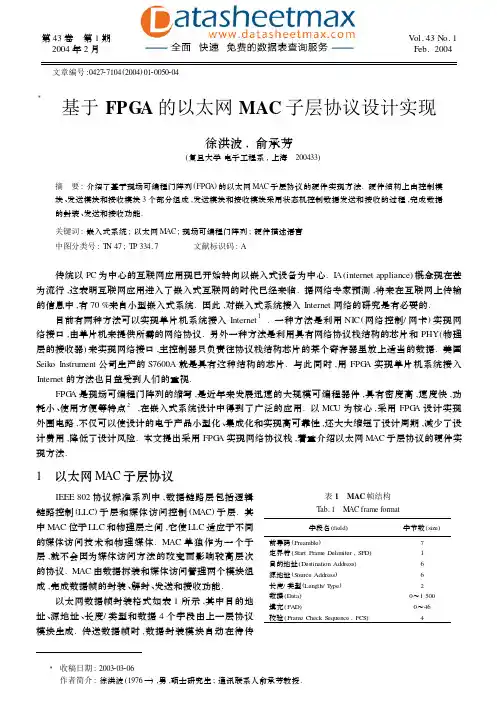
第43卷 第1期2004年2月复旦学报(自然科学版)Journal of Fudan University (Natural Science )Vol.43No.1Feb.2004 文章编号:042727104(2004)0120050204Ξ基于FPGA 的以太网MAC 子层协议设计实现徐洪波,俞承芳 (复旦大学电子工程系,上海 200433)摘 要:介绍了基于现场可编程门阵列(FPG A )的以太网M AC 子层协议的硬件实现方法.硬件结构上由控制模块、发送模块和接收模块3个部分组成,发送模块和接收模块采用状态机控制数据发送和接收的过程,完成数据的封装、发送和接收功能.关键词:嵌入式系统;以太网M AC ;现场可编程门阵列;硬件描述语言中图分类号:T N 47;TP 334.7 文献标识码:A传统以PC 为中心的互联网应用现已开始转向以嵌入式设备为中心.I A (internet appliance )概念现在甚为流行,这表明互联网应用进入了嵌入式互联网的时代已经来临.据网络专家预测,将来在互联网上传输的信息中,有70%来自小型嵌入式系统.因此,对嵌入式系统接入Internet 网络的研究是有必要的.目前有两种方法可以实现单片机系统接入Internet 1.一种方法是利用NIC (网络控制/网卡)实现网络接口,由单片机来提供所需的网络协议.另外一种方法是利用具有网络协议栈结构的芯片和PHY (物理层的接收器)来实现网络接口,主控制器只负责往协议栈结构芯片的某个寄存器里放上适当的数据.美国Seiko Instrument 公司生产的S7600A 就是具有这种结构的芯片.与此同时,用FPG A 实现单片机系统接入Internet 的方法也日益受到人们的重视.FPG A 是现场可编程门阵列的缩写,是近年来发展迅速的大规模可编程器件,具有密度高,速度快,功耗小、使用方便等特点2,在嵌入式系统设计中得到了广泛的应用.以MC U 为核心,采用FPG A 设计实现外围电路,不仅可以使设计的电子产品小型化、集成化和实现高可靠性,还大大缩短了设计周期,减少了设计费用,降低了设计风险.本文提出采用FPG A 实现网络协议栈,着重介绍以太网M AC 子层协议的硬件实现方法.1 以太网MAC 子层协议表1 MAC 帧结构T ab.1 M AC frame format 字段名(field )字节数(size )前导码(Preamble )7定界符(S tart Frame Delimiter ,SFD )1目的地址(Destination Address )6源地址(S ource Address )6长度/类型(Length/T ype )2数据(Data )0~1500填充(PAD )0~46校验(Frame Check Sequence ,FCS )4 IEEE 802协议标准系列中,数据链路层包括逻辑链路控制(LLC )子层和媒体访问控制(M AC )子层.其中M AC 位于LLC 和物理层之间,它使LLC 适应于不同的媒体访问技术和物理媒体.M AC 单独作为一个子层,就不会因为媒体访问方法的改变而影响较高层次的协议.M AC 由数据拆装和媒体访问管理两个模块组成,完成数据帧的封装、解封、发送和接收功能.以太网数据帧封装格式如表1所示,其中目的地址、源地址、长度/类型和数据4个字段由上一层协议模块生成.传送数据帧时,数据封装模块自动在待传Ξ收稿日期:2003203206作者简介:徐洪波(1976—),男,硕士研究生;通讯联系人俞承芳教授.输数据前面添加7个字节的前导码和1个字节的定界符,并在数据传送结束时加发4个字节的循环冗余校验码,如果数据长度小于46字节,则会自动进行数据填充以达到要求的最短长度.接收数据帧时,数据拆装模块将自动丢弃前导码和定界符2个字段.媒体访问管理模块主要实现CS M A/C D (carrier sense multiple access with collision detection )协议3.CS 2M A/C D 是一种分布式介质访问控制协议,使网中的多个站(节点)可以共享传输介质.发送数据帧时,节点首先进行载波监听,当介质空闲时开始发送帧.如果在传输过程中与其他节点产生冲突,则正在传输的每个节点必须发出32比特大小的阻塞信号来加强冲突,以便通知总线上各个站点已发生冲突,然后随机延时一段时间重新争用介质,再重新传送数据帧.2 MAC 子层协议的FPG A 实现以太网M AC 子层协议的硬件结构框图如图1所示,由控制模块、发送模块和接收模块3个部分组成.由于小型嵌入式系统主要应用在集散控制系统中,信息交流多为“一问一答”式的半双工通信模式,同时为了降低硬件资源的开销,本模块仅支持半双工通信模式.图1 硬件结构框图Fig.1 Hardware architecture2.1 控制模块该模块包含主机接口、寄存器、发送数据缓冲区及接收数据缓冲区4个部分.主机接口部分用以实现与MC U 之间的数据交换,采用8位外部数据总线.寄存器主要用于功能参数的设置及状态信息的存贮.发送数据缓冲区是主机与发送模块之间的数据传输通道,接收数据缓冲区则是主机与接收模块之间的数据传输通道.控制模块的工作时钟有两种选择方式,一种是直接由外部提供,另一种是外部时钟通过FPG A 片内的延迟锁相环进行倍频后供内部使用,用户可以根据系统设计实际需要自由选择.数据缓冲区(发送数据缓冲区和接收数据缓冲区)用作发送与接收数据的缓冲,以使主机的传输速度与本模块相匹配.发送数据时,主机先将待发送的数据帧写入发送数据缓冲区,然后由发送模块将数据读出.传统意义上的数据缓冲区由一块内部或外部RAM 来实现,但这样需要设计实现一个复杂的控制状态机来管理主机、发送模块和接收模块3个部分对RAM 的读写.S partan Ⅱ系列的FPG A 内部提供了丰富的块RAM 资源,可以配置双端口RAM.因此本文将发送缓冲区分成两个独立的部分,这样每个数据缓冲区便可以由双端口的RAM 来实现,大大简化了设计,节省了硬件资源.2.2 发送模块该模块主要实现CS M A/C D 协议,完成数据帧的传送,即以字节为单位从发送缓冲区读取数据,并将其转换成4比特的半位元传送给以太网的物理层PHY 芯片,结构框图如图2(见第52页)所示.重发计数器用以存贮当前帧成功传输时的发送次数.帧间隙计数器用以保证相邻两个帧之间保持一15第1期 徐洪波等:基于FPG A 的以太网M AC 子层协议设计实现图2 发送模块结构框图Fig.2 Diagram of sending m odule定的传输时间间隔.冲突窗计数器用以判断当前所发生的冲突是否为后冲突(late collision ).延时计数器用以存贮启动传输后等待总线空闲的时间,当超过一定时间后将放弃当前帧的传输.这4个功能子模块都由1个计数器和1个比较器来实现.退避计数器模块用以实现二进制指数退避算法,包括一个伪随机数生成器.CRC 生成电路用以实现数据帧的校验码序列,采用4位数据线并行方式实现4.发送控制状态机是整个发送模块的核心,用以管理各个功能子模块,并使它们按照一定的时序协同工作,其状态图如图3所示.当总线被其他站点占用进行数据传输时,发送模块处于Defer 状态,如果此时数据准备好需要传输则启动延时计数器,经过规定的最大延时时间后总线仍被占用则放弃当前帧的传输.当总线空闲后则进入IPG 状态,经过最小帧间间隙时间自动进入空闲状态I D LE 并等待数据传输,此时如果数据准备好并且数据的长度大于46字节则按照前导码、数据、校验序列的顺序进行数据帧的传输,否则按照前导码、数据、数据填充、校验序列的顺序进行数据帧的传输;在传输过程中,如果遇到冲突则进入Jam 状态,发达32比特的阻塞信号加强冲突以保证网络的各个站点都可以检测到此次的冲突,如果此次冲突是后冲突则直接进入Defer 状态,并丢弃当前帧,否则进入Back 状态,随机延时一段时间后重新争用总线来传输当前帧.图3 发送控制状态机Fig.3 S tate machine of sending m odule2.3 接收模块图4 接收模块结构框图Fig.4 Diagram of receiving m odule 该模块主要完成数据帧的接收,即从物理层PHY 芯片接收4比特半位元数据,将其转化成以字节为单位的数据并存贮在接收数据缓冲区,结构框图如图4所示.地址判断子模块用以检查帧的目的地址字段是否与本站地址相匹配,如果不匹配,则说明不是发送给本站的而将它丢弃掉.帧间隙计数器用以检测接收到的数据帧与前一帧之间是否满足最小帧间间隔的要求,如果不满足则将它丢弃.接收字节计数器用以存贮接收帧的字节长度,判断接收帧长度是否满足要求(在最小帧长度与最大帧长度之间).CRC 生成电路与发送模块一样采用4位数据线并行方式实现.接收控制状态机是整个接收模块的核心,负责管理各个功能子模块,检测总线及实现接收数据帧的时序,其状态图如图5所示.通常接收模块处于I D LE 状态并监听总线的状态,当检测到以太网帧的前导码25复旦学报(自然科学版) 第43卷时自动进入SFD 状态,此时如果接收到以太网数据帧的帧定界符,并且与前一个数据帧之间的时间间隔大于最小帧间间隙,则接收模块进入数据接收状态开始接收数据.处于Data0状态时接收字节的低4位,而处于Datal 状态时接收字节的高4位,并在Data0状态将接收到的完整字节数据存贮到接收数据缓冲区.如果接收的数据字节数超过允许的最大帧长度,则接收模块进入Drop 状态,此时丢弃后面的数据.当全部数据传输完毕即总线处于空闲时,接收模块重新处于I D LE 状态,等待接收下一个数据帧.图5 接收控制状态图Fig.5 S tate machine of receiving m odule3 综合与仿真本文采用X ilinx 公司的S partan Ⅱ系列XC2S100PQ208芯片,整个设计全部采用Verilog H D L 硬件描述语言5来实现,并在F oundation 3.1的设计平台上完成整个模块的设计、综合、仿真、映射及布局布线.图6为发送时序仿真的波形,从图中可以看出,当传输过程中发生冲突时继续发送32比特的阻塞码,然后随机延时一段时间重新争用介质以传输数据,这说明本模块满足了CS M A/C D 协议.图6 发送时序仿真波形Fig.6 T iming simulation of transmission with collision本文介绍了一种简易的基于FPG A 的以太网M AC 子层协议的设计方法.通过本模块可以简单方便地实现小型嵌入式系统的Internet 网络接口,如果再结合基于FPG A 实现的TCP/IP 协议栈及其他辅助功能模块,不仅可以使小型嵌入式系统接入网络更加简单,而且系统的集成度、稳定性将进一步得到提高. 参考文献:1 王 兰,王景存,杨 君.单片机系统接入Internet 方法的探讨J .电子技术,2002,29:37238.2 朱明程.数字系统现场集成技术M.南京:东南大学出版社,2001.3 IEEE S td 802.3,2000Edition ,Part 3:Carrier sense multiple access with collision detection (CS M A/C D )access method and physical layer apecifications S.4 Shieh M D ,Sheu M H ,Chen C H ,et al .A systematic approach for parallel CRC computations J .Journal o f Infor 2mation Science and Engineering ,2001,17:4452461.5 Bhasker J.Verilog H D L 硬件描述语言M.北京:机械工业出版社,2000.(下转第61页)35第1期 徐洪波等:基于FPG A 的以太网M AC 子层协议设计实现11 D ominguez 2Castro R ,Espejo S ,R odriguez 2V ′azques A ,et al .A 0.8-m C M OS 22D programmable mixed 2signal focal 2plane array 2process or with on 2chip binary imaging and instructions storage J .IEEE J Solid 2State Circuits ,1997,32:101321026.12 Cruz J M ,Chua L O ,R oska T.A fast ,complex and efficient test implementation of the C NN universal machine A.Proc Third IEEE In W orkshop Cellular Neural Netw orks and Application (C NNA 294) C.R ome :IEEE ,1994.61266.GVF Implementation of Multilayer CNN and ItsApplication to Image SegmentationHUAN G Xu 2ming ,ZHOU Dong 2ming ,ZH AN G Li 2ming(Department o f Electronic Engineering ,Fudan Univer sity ,Shanghai 200433,China )Abstract :An implementation method of G VF field using multilayer cellular neural netw orks (C NN )is proposed ,which is com 2bined with expanded and thinned m odel of C NN to realize the image segmentation strategy of active contours.The C NN has par 2allel processing ability.Therefore it not only s olves the problem of computational comlexity of G VF field using traditional serial computation ,but als o av oids the local minimum in C NN active contours.G uided by G VF in formation ,external image will be e 2v olved until it reaches the desired position.The experiment results show that the proposed method is better than that of Vilari 2no ,et al ,for different input images and it als o has real time processing speed.K eyw ords :image process ;image segmentation ;cellular neural netw orks (C NN );active contour (Snake );gradient vector flow (G VF )~~~~~~~~~~~~~~~~~~~~~~~~~~~~~~~~~~~~~~~~~~~~~~~~~~~~(上接第53页)Implementation of Ethernet MAC B ased on FPGAXU Hong 2bo ,Y U Cheng 2fang(Department o f electronic Engineering ,Fudan Univer sity ,Shanghai 200433,China )Abstract :The implementation of the E thernet M AC based on FPG A is briefly presented.The hardware architecture consists of control m odule ,sending m odule and receiving m odule.The sending m odule and the receiving m odule are controlled by a state machine and implement the function of data encapsulation ,sending and receiving.K eyw ords :Embedded 2system ;E thernet M AC ;FPG A ;H D L 16第1期 黄旭明等:G VF 场的多层细胞神经网络实现及其在图像分割中的应用。
一种基于FPGA的万兆以太网MAC层设计与实现作者:安超群李飞来源:《无线互联科技》2023年第18期作者简介:安超群(1986—),女,湖北襄阳人,工程师,硕士;研究方向:模拟电路设计,集成电路设计,数字信号处理,可靠性设计等。
摘要:针对基于软件设计的万兆以太网MAC层无法满足高速数据实时传输的发展要求,文章提出了一种基于FPGA硬件平台的万兆以太网MAC层协议的设计与实现方案。
该设计方案主要利用FPGA的并行处理能力,通过Verilog硬件描述语言完成万兆以太网MAC层数据实时处理的硬件设计,实现大带宽、低延时和高可靠性的万兆以太网MAC层的数据收发功能。
试验验证表明:该设计方案实现了万兆以太网高速率的数据传输,具有低延时、高性能、高可靠性与简易性等优点。
关键词:万兆以太网;MAC控制器;并行CRC校验;并行数据处理中图分类号:TP311 文献标志码:A0 引言以太网(Ethernet)是一种计算机局域网技术。
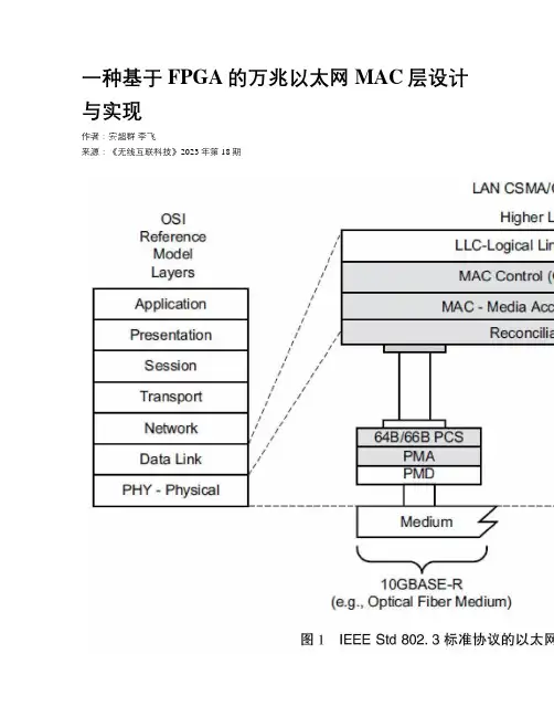
IEEE制定的IEEE Std 802.3协议,规定了包括MAC层的协议内容、电信号以及物理层的连线。
从1983年第一次发布IEEE Std 802.3协议至今,以太网经过了40年的发展,传输速率从10 Mbps、100Mbps提升到1 000Mbps,目前已经达到了10 Gbps[1]。
万兆以太网是也称10 G以太网(10 Gigabit Ethernet),是在IEEE802.3ae协议中提出的以太网标准,该标准规范中规定使用光纤传输、传输带宽高达10 Gbps、传输距离最远能达到40km [2],经过不断的升级与扩充,万兆以太网以其速率高、兼容性好、稳定性强的优点逐渐成为以太网的核心设备[3],服务于工业自动化、5G网络传输和智慧城市建设等行业。
大多数系统设计中,10Mbps、100Mbps和1 000Mbps以太网协议除了物理层以外的协議层均以软件的方式实现,甚至10 Gbps以太网协议使用高性能CUP或服务器实现。
基于FPGA的MAC协议设计与开发随着物联网应用场景的不断发展和普及,越来越多的设备需要通过网络进行通讯和协作。
而在通信网络中,MAC层协议扮演着重要的角色,是连接网络各个设备的关键。
因此,基于FPGA的MAC协议设计与开发,成为了当前研究的热点之一。
一、FPGA概述FPGA(Field Programmable Gate Array),即现场可编程门阵列,是半导体电路设备中的一种。
FPGA通过集成数百万至数千万个可编程电路单元,并提供了更灵活的接口,实现了在硬件级别上的编程。
FPGA硬件级别上的可编程性,使其在通讯领域、嵌入式系统以及数字信号处理等技术领域得到广泛的应用。
二、MAC协议概述MAC(Media Access Control)协议是通讯网络中,用来控制多个设备在同一媒介上的共享和使用。
MAC协议中,常用的是CSMA/CD协议(载波侦听多路访问/碰撞检测)和CSMA/CA协议(载波侦听多路访问/碰撞撞消)。
其中,CSMA/CD协议适用于有线网络环境,而CSMA/CA协议适用于无线网络环境。
三、基于FPGA的MAC协议设计与开发,是通过对硬件级别进行编程实现的。
与传统以软件为主的实现方式相比,基于FPGA的开发具备硬件级别上的并行处理能力,可以实现更高的数据传输速度和更低的延迟。
同时,基于FPGA的开发还能有效降低系统的功耗与成本。
在实际的设计过程中,需要根据具体的应用场景,对MAC协议进行设计与优化。
例如,对于高速局域网环境,需要通过对协议码进行优化,实现更高效的数据传输。
而对于低功耗的无线传感器网络,需要通过调整功耗控制策略,实现更长的网络寿命。
基于FPGA的MAC协议设计与开发,可以通过VHDL等硬件描述语言进行实现。
同时,也可以借助数学建模和仿真等方法进行验证。
在具体实现时,需要科学合理地进行设计,并考虑到可靠性和可拓展性等关键因素,以实现高效的数据传输和系统稳定性。
四、结语基于FPGA的MAC协议设计与开发,是通讯网络领域的一个热点研究方向。
邮局订阅号:82-946360元/年技术创新PLD CPLD FPGA 应用《PLC 技术应用200例》您的论文得到两院院士关注一种以太网MAC 控制器的FPGA 实现方法An Implementation Approach Of Ethernet MAC Controller On FPGA(1.电子科技大学2.中国科学院微电子研究所)尉志伟1,2赵建明1吴斌2WEI Zhi-wei ZHAO Jian-ming WU Bin摘要:介绍了一种10M/100M 以太网MAC 控制器的FPGA 实现方法,对包括全功能的MAC 控制器系统架构、工作机制进行了解析,提出了一种基于读指针可载入的异步FIFO 的帧缓存结构,便于实现坏帧丢弃和冲突帧重传,与传统的缓存结构相比提高了片内缓存的利用效率。
设计已经通过RTL 仿真验证及FPGA 系统验证。
关键词:802.3MAC;读地址可载入;缓存结构;嵌入式IP 中图分类号:TP393.11文献标识码:AAbstract:An implementation approach of 10M/100M Ethernet MAC controler based on FPGA is introduced.The system architecture and work principle of full_function MAC controller is then analyzed.A type of read_pointer_loadable asychronous FIFO architecture is presented,which has been used in MAC buffer architecture pared with traditional buffer architecture,this approach can raise the usage efficiency of in_chip memory and can implement bad frame dropping and collied frame retransmition function of the MAC controller easily.The designed MAC controller has been tested in RTL level and been validated on FPGA development board.Key words:802.3MAC;read_pointer_loadable;buffer architecture;embeded IP文章编号:1008-0570(2010)12-2-0131-03引言在网络日益丰富的今天,网络传输是最经济有效的数据传输方式。
基于FPGA的以太网MAC控制器的设计与实现丁世勇;谭文文;李桂英【摘要】The design of Ehernet MAC controller based on FPGA is described. The controller realizes the CSMA/CD (Carrier Sense MultipleAccess/Collision Detection)protocol in half duplex mode and the transmitting and receiving of Pause frame in full duplex mode, and it can access the register in the physical chip. The whole design is described in a way of top-down design flow with Verilog hardware description language. We simulated the design with Modelsim and verified it with FPGA board. The test result shows that the design can satisfy the requirement of 802.3 standard.%介绍了基于FPGA的以太网MAC控制器的设计,主要实现了半双工模式下CSMA/CD协议、全双工模式下Pause帧的收发,以及对物理层芯片中寄存器的读写访问。
设计采用Verilog硬件描述语,按照自顶向下的设计流程描述了以太网的主要功能模块,该控制器通过Modelsim进行了仿真并进行了FPGA板级验证,验证其能够满足802.3标准的要求。
【期刊名称】《电子设计工程》【年(卷),期】2011(019)021【总页数】4页(P163-165,169)【关键词】以太网;FPGA;Verilog;HDL;Modelsim;MAC控制器【作者】丁世勇;谭文文;李桂英【作者单位】山东科技大学信息与电气工程学院,山东青岛266510;山东科技大学信息与电气工程学院,山东青岛266510;山东科技大学理学院,山东青岛266510【正文语种】中文【中图分类】TN492随着网络的飞速发展,因特网(Internet)在人们的生活中占据着越来越重要的地位。
MAC 在FPGA 中的高效实现曹 琦 毕笃彦 张 齐(空军工程学院信号实验室,陕西 西安 710038)摘 要: 乘累加器在DSP 算法中有着举足轻重的地位。
现在,很多前端DSP 算法都通过FPGA 实现。
结合FPGA 具体的硬件结构,提出了乘累加器在FPGA 中实现的改进方法:流水线技术、CSD 编码、DA 算法,最后给出了这几种方法的实验结果。
结果表明,这些方法的应用能大幅度的提高乘累加器在FPGA 中的运行性能。
关键词: 乘累加器 流水线 CSD 编码 DA 算法中图分类号:TN929.533 文献标识码:BThe High Efficient Realization of MAC with FPGACao-Qi, Bi Du-yan ,Zhang-Qi(Signal Lab of Department 4, A.F. Engineering College, Xi’an 710038)Abstract: MAC plays a very important role in DSP algorithms. Nowadays ,many front-side DSP algorithms are achieved through FPGA. Based on the specific hardware structure of the FPGA, this paper puts forward several methods to improve the achievement of MAC in FPGA. These methods include: pipeline technology, CSD encoding and DA algorithm. Then this paper provides the experimental results of these methods. It is concluded that they can greatly improve the performance of MAC in FPGA.Keyword: MAC, Pipeline, CSD encoding, DA algorithm1 引言当今,现场可编程逻辑门阵列FPGA 成为数字信号处理技术的前沿。
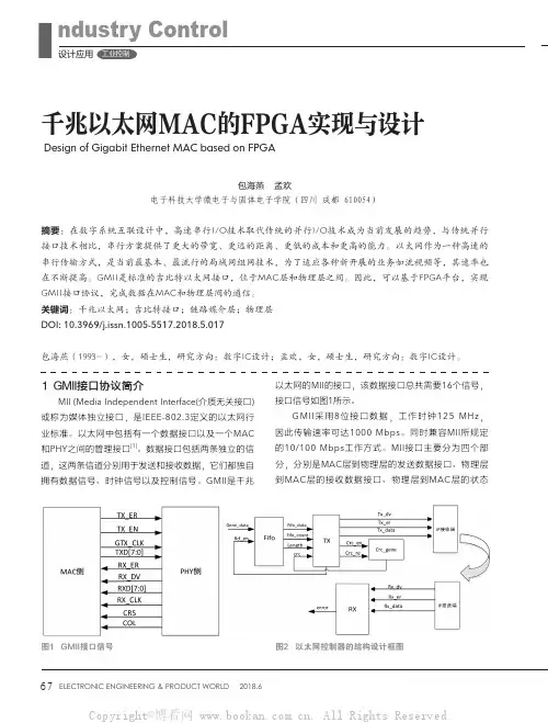
图1 GMII接口信号图2 以太网控制器的结构设计框图6774ELECTRONIC ENGINEERING & PRODUCT WORLD2018.6指示接口、MAC层和物理层的控制和状态信息接口(MDIO)。
具体的信号说明如表1所示。
2 设计方案X i l i n x提供的千兆以太网开发套件为Vi rt e x-5 ML505/ML506开发板,该开发板支持10/100 M、1/10 G以太网,是学习和研发高速连接设备的理想平台。
Xilinx提供了可参数化的10/1 Gbps以太网物理层控制据送出去。
接收数据则与之相反2.1 电路架构该以太网控制器主要进行层协议的接口以及MAC计,总体结构框图如图据的产生模块、发送模块层编解码模块、接收及校验模块分。
发送模块和接收模块主要提供图3 CRC8编码的串行实现图4 GMII的传输格式图5 MAC控制器中的状态转移图3 电路实现与仿真3.1 MAC发送端-数据成帧号,与主机接口从外部存储单元获取的发送数据按照标准协议进行封装,空闲时发送给PHY 层转换发送到网络中去在物理层部分BASE-X PCS/PMA IP CORE 核支持内部或外部链接。
IP 核内的主要组成部分为为物理层的媒介层,图6 接收端数据提取时序图图7 电路的仿真波形图信号I/O 描述TX_ER O 发送器错误信号TX_EN O 发送器使能信号GTX_CLK O 吉比特发送信号的时钟(125 M )TXD O 被发送的数据RX_ER I 接收数据出错指示RX_DV I 接收数据有效指示RXD I 接收数据RX_CLK I 接收时钟信号CRS I 载体感应,仅用于半双工COL I 冲突检测,仅用于半双工表1 CMII接口信号描述[2]王春华.Xilinx可编程逻辑器件设计与开发(基础篇).[M]北京:人民邮电出版社,2011.[5]王长清.基于FPGA的千兆以太网通信板卡的设计与实现[D].河南:河南师范学报,2011.[1]Jeff Watson,Gustavo Castro.高温电子设备对设计和可靠性带来挑战[J].模拟对话,2012,4.[2]Jeff Watson,Maithil Pachchigar.面向高温应用的低功耗数据采集解决方案[J].模拟对话,2015,8.[3]CN-0365:面向高温环境的16位、600 kSPS、低功耗数据采集系统,ADI公司,2015,6.[4]Alan Walsh.面向精密SAR模数转换器的前端放大器和RC滤波器设计[J]模拟对话,2012,12.[5]John L. Evans,James R.Thompson,Mark Christopher,etc.不断变化的汽车环境:高温电子设备。
基于FPGA的I2 C控制器的实现王龙飞;郎宝华【摘要】文中旨在研究具有接口线少、控制方式简单、器件封装形式小、通信速率较高等优点的 I2 C 总线,所以选取了SAA7113作为视频解码芯片。
文章简述了I2 C总线协议的数据传输时序,及模拟视频解码芯片SAA7113的基本功能、工作原理和相关寄存器的设置,给出基于FPGA的SAA7113初始化的方法,并且详细的概述了I2 C总线的各个模块,在寄存器配置中给出了相应的芯片初始化的状态转换图,最后用Quartus软件进行仿真,实验证明数据传输符合I2 C协议规定。
结果证明可以正确的配置芯片,进行视频数据的采集。
%The purpose is to study the I2C bus,it has the interface cable and control simple devices are packaged in small,higher commu-nication speed,etc,so select the SAA7113 as video decoder chip. It gives a brief account of the data transmission timing of the I2C bus protocol,the basic functions of the analog video decoding chip SAA7113 works and associated register set,and presents a SAA7113 ini-tialization approach based on FPGA,overviews each module of the I2C bus in detail,and is given in the register configuration of the chip initialization state transition diagram,finally use the Quartus software for simulation,the experiments show that data transmission complies with the provisions of the I2C protocol. The results show that correctly configure the chip,and have video data collection.【期刊名称】《计算机技术与发展》【年(卷),期】2013(000)003【总页数】4页(P227-230)【关键词】I2C总线;SAA7113;FPGA【作者】王龙飞;郎宝华【作者单位】西安工业大学电子信息工程学院,陕西西安 710021;西安工业大学电子信息工程学院,陕西西安 710021【正文语种】中文【中图分类】TP390 引言I2C 总线[1](Inter Integrated Circuit)是飞利浦公司于20 世纪80 年代开发的一种“电路板级”的总线结构。

MAC在FPGA中的高效实现
曹琦;毕笃彦;张齐
【期刊名称】《微计算机信息》
【年(卷),期】2007(023)017
【摘要】乘累加器在DSP算法中有着举足轻重的地位.现在,很多前端DSP算法都通过FPGA实现.结合FPGA具体的硬件结构,提出了乘累加器在FPGA中实现的改进方法:流水线技术、CSD编码、DA算法,最后给出了这几种方法的实验结果.结果表明,这些方法的应用能大幅度的提高乘累加器在FPGA中的运行性能.
【总页数】3页(P216-218)
【作者】曹琦;毕笃彦;张齐
【作者单位】710038,陕西西安,空军工程学院信号实验室;710038,陕西西安,空军工程学院信号实验室;710038,陕西西安,空军工程学院信号实验室
【正文语种】中文
【中图分类】TN929.533
【相关文献】
1.LTE基站中PDSCH高效并行计算的FPGA实现 [J], 廖晓强;钱俊伟;朱宇霞
2.用FPGA实现的具有过滤报文功能的Mac在电力系统中的应用 [J], 沈峻
3.RPR中MAC处理单元的FPGA实现 [J], 柳利军;熊良芳
4.B3G系统中基于FPGA的高速MAC设计与实现 [J], 李振华;吴俊
5.WCDMA系统中Turbo码译码器的FPGA实现——高效实现Log-MAP算法的硬件结构 [J], 姜军;白春龙;张平;胡健栋
因版权原因,仅展示原文概要,查看原文内容请购买。
用FPGA实现MAC核所要完成的功能用FPGA实现MAC核所要完成的功能MAC发送模块MAC发送模块可将上层协议提供的数据封装之后通过MII接口发送给PHY。
发送模块可接收主机接口模块的数据帧开始和数据帧结束标志,并通过主机接口从外部存储器中读取要发送的数据,然后对数据进行封装,然后通过PHY提供的载波侦听和冲突检测信号,在信道空闲时通过MII接口将数据以4位的宽度发送给PHY,最后由PHY将数据发送到网络上。
发送模块由CRC生成模块(crc_gen)、随机数生成模块(random_gen)、发送计数模块(tx_cnt) 和发送状态机(tx_statem_模块等四个子模块组成。
CRC生成模块(crc_gen)该模块用于计算发送数据的CRC值,并将CRC值添加到数据帧的帧校验序列字段(FCS)内。
为了提高效率,并考虑到MAC与PHY的数据通道为4位,设计时可采用4位并行CRC计算方法,算法中可使用一个次态函数,并通过循环迭代来模拟移位操作。
这样,发送模块就可以在边发送数据到PHY的同时,一边计算CRC,这样当数据发送完时,CRC值也计算完成了。
随机数生成模块(random_gen)如在发送过程中检测到冲突,发送模块就先发送拥塞码(jam),随后停止发送。
在下次重新发送之前,发送模块会先执行一个后退(backoff)操作,即发送模块等待一个半随机(生成的随机数有范围限制)的时间之后再开始发送。
该随机数就是由随机数生成模块产生的,它采用经典的截断二元指数后退算法,后退的时间是一个与发生冲突次数有关的随机数,随着冲突的次数增多,用于生成该随机数的范同也将逐渐增大,以减少冲突的概率。
发送计数模块(tx_cnt)发送计数模块由半字节计数器(nibcnt)、字节计数器和重试次数计数器(retrycnt)三个计数器组成。
其中重试次数计数器(retrycnt)可对发送某个帧时产生冲突次数进行计数。
当计数器的值达到最大重试次数时,它将放弃重试,并丢弃发送缓冲器内的数据。
基于FPGA的以太网MAC控制器的实现
王时雨;贺占庄;张盛兵
【期刊名称】《微电子学与计算机》
【年(卷),期】2012(29)2
【摘要】以太网IEEE802.3协议根据LAN的特点,把数据链路层分成LLC(逻辑链路控制)和MAC(介质访问控制)两个子层.MAC层协议作为数据帧收发的基础,是以太网技术的核心,主要负责上层数据和物理层的数据流量控制和数据流的检测、校验工作.介绍了基于FPGA的10MHz/100MHz以太网MAC控制器的设计,整个设计用Verilog语言实现.自主设计开发验证板,使用Altera厂商的
FPGA(EP1C20F400C8)并验证.
【总页数】5页(P171-175)
【关键词】MAC协议;FPGA;Verilog
【作者】王时雨;贺占庄;张盛兵
【作者单位】西北工业大学软件与微电子学院;西安微电子技术研究所
【正文语种】中文
【中图分类】TP393
【相关文献】
1.基于FPGA的以太网MAC控制器的设计与实现 [J], 丁世勇;谭文文;李桂英
2.以太网MAC控制器的FPGA实现 [J], 郭航
3.标准802.3以太网MAC控制器的FPGA设计与实现 [J], 龚坚;彭晖;乔庐峰;朱
勇
4.万兆以太网MAC层控制器的FPGA设计与实现 [J], 张友亮;刘志军;马成海;赵艳艳;张风
5.一种以太网MAC控制器的FPGA实现方法 [J], 尉志伟;赵建明;吴斌
因版权原因,仅展示原文概要,查看原文内容请购买。
RPR中MAC处理单元的FPGA实现
柳利军;熊良芳
【期刊名称】《光通信技术》
【年(卷),期】2005(029)005
【摘要】弹性分组环(Resilient Packet Ring)桥接芯片是弹性分组环技术在光通信领域得以运用的关键芯片,MAC地址处理是桥接芯片的一个必备的功能.分析了RPR中适用的HASH算法,介绍了MAC处理单元在FPGA中实现方法,并给出了仿真验证结果.
【总页数】3页(P39-41)
【作者】柳利军;熊良芳
【作者单位】武汉科技大学城建学院电工教研室,武汉,430070;中兴通讯股份有限公司,深圳,518004
【正文语种】中文
【中图分类】TN915
【相关文献】
1.FPGA实现信号处理单元中的存取管理算法 [J], 张留安;田斌;易克初
2.基于RPR业务流统计部分的FPGA实现 [J], 李季碧;张治中;黄士广
3.RPR MAC数据通路的设计与实现 [J], 史晓飞;李惠军;李玲;马骞
4.基于FPGA的图像预处理单元的硬件实现 [J], 朱喜;王玲;郑善贤;郭湘勇
5.浮点乘累加处理单元的FPGA实现 [J], 金席;高小鹏;龙翔
因版权原因,仅展示原文概要,查看原文内容请购买。
I.J.Mathematical Sciences and Computing,2016, 4, 24-33Published Online November 2016 in MECS ()DOI: 10.5815/ijmsc.2016.04.03Available online at /ijmscImplementation of Fast and Efficient Mac Unit on FPGASachin Raghav a, Dr. Rinkesh Mittal aa CEC Landran, Mohali/ECE Dept, Chandigarh, 140307, IndiaAbstractFloating-point arithmetic operations on digital systems have become an important aspect of research in recent times. Many architecture have been proposed and implemented by various researchers and their merits and demerits are compared. Floating point numbers are first converted into the IEEE 754 single or double precision format in order to be used in the digital systems. The arithmetic operations require various steps to be followed for the correct and accurate steps. In the proposed approach a fast and area efficient Carry Select Adder are implemented along with the parallel processing of various units used in the architecture. The result also verifies the proposed approach that shows a decrement of 27 % in the combinational path delay with an increment of around 8% in the number of LUTs used.Index Terms: MAC Unit, FPGA, FMA.© 2016 Published by MECS Publisher. Selection and/or peer review under responsibility of the Research Association of Modern Education and Computer Science1.IntroductionIn DSP applications the floating-point FMA instruction is currently available in many general-purpose processors. It enhances its performance by decreasing the latency factor and increases the level of accuracy with no intermediate routing. Most of the processors like intel, IBM has involves the fused multiply fused unit in its FP units in order to carry out double precision FMA operation. This FMA operation is significant when an FP multiplication is followed by FP addition. It has the capability to enhance the arithmetic precision of algorithm as rounding steps have reduced. FMA is also helped to improve the performance as it implements FMA instructions which have shorter latencies than floating point multiply and floating point add sequences. FMA implementation has two advantages. The first advantage is that the FMA operation is performed with only one rounding instead of two which helps to reduce overall error due to rounding and another advantage is that it reduces delay and hardware required by sharing components.In the year 1990, the first floating-point FMA unit was introduced on IBM RISC System/6000 that is used for single instruction execution operation as an indivisible operation. In basic FMA unit FADD and FMUL executions is not possible. The development of FMA architecture utilizes the multiplier array followed by * Corresponding author.E-mail address: sachin.raghav219@, hod.coeece@.inalignment blocks. Thus, the range of input of the multiplier tree should be expanded because of the huge variable multiplier tree is necessary. Some explanation has been detected in Lang/Bruguera FMA architecture that is developed for minimizing the latencies. FP operation is utilized for some real time applications in multimedia and graphics and also in DSP processor. as it gives extensive range of real numbers. Many new processors execute FP operation according to IEEE 754-1985 standards.2.Literature ReviewHan, Liu, HaoZhang et al. [1] in this paper, fused multiply-add function has been presented. This proposed method is used to increase the speed of Decimal floating-point. Specific decimal redundant encoding system has applied to the fused multiply add architecture. This proposed approach is compared with other architecture and its results demonstrated that speed is increased about 33.7%.Pande, Kuldeep et al. [2] presented mutual procedure of floating point division. The objective of this work is to enhance the presentation and precision of application where this procedure was applied. The divide adds fussed unit provides the same architecture to the floating point but divider makes some difference as it is executed by utilizing digit-recurrence method. This works indicates that presented architecture has improved precision as compared to its units such as divider unit and adder unit. This architecture is appropriate for less latency, precision, and its price. The presented architecture is implemented using 4vfx60ff672-12 Xilinx Spartan-6 FPGA.Kakde, Sandeep, Mithilesh Mahindra et al. [3] this paper developed a Multiplier by utilizing reduced complexity Wallace Multiplier to reduce the latency. In this work, the average delay of proposed approach is 37.673ns. Normalization and Alignment Shifter has also been designed using barrel shifter. In order to obtain the higher precision and lower latency, this shifter has been designed. The total delay is found to be 5.845 ns for this shifter.Manolopoulos, K., D. Reiss et al. [4] presented multi-functional, multiple precision floating-point Multiply-Add Fused (MAF) unit. The proposed multiply-add fused unit is capable of performing a quadruple accuracy. In this work, implementation of proposed design is done on a 65 nm silicon process attaining highest operating frequency of 293.5 MHz at 381 mW power.He, Jun, Ying Zhu et al. [5] presented Design of a quadruple floating-point FMA unit. The proposed design supports multiple floating-point arithmetics with a 7 cycles pipeline. The implementation is done on 65nm technology and works at 1.2 GHz with reduces by 3 cycles. Also, the gate number decreased by 18.77% and the frequency increased about 11.63%.Lupon, Marc, EnricGibert et al.[6] presented a new hardware /software collaborative approach which is capable of performing workloads with improved utilization of fused multiply -adder. the host ISA of a hardware /software processor has been extended with a new CMA instruction that executes an FMA procedure with an intermediate rounding.Bruguera, Javier D et al. [7] In this work a design for double precision floating point FMA unit has been presented. This computation based on FMA operation A + (B ×C) which allows to calculating FP addition with less latency than FP multiplication and multi[ly-add fused. This novel architecture allows skipping pipeline stage which is first step. This first step is related with multiplication B*C. for a multiply-add fused unit (MAF) unit pipelined into three or five stages.AtishKhobragade,et al. [8] In this paper 128-Bit Fused Multiply Add Unit has been proposed for a crypto processor. this fused multiply add unit has been executed on the FPGA(field programmable gate array).the major goal of this work is to decrease latency. It is found that latency gets decreased up to 25%. In order to obtain the higher accuracy, normalization and alignment shifter has been developed in MAF unit. Dhanabal, R. et al. [9]an improved design for Floating-Point FMA unit has been proposed in this paper. This architecture is usually used for less power and condensed area applications. The fused unit, floating-point (A ×B) + C operation has been computed in a single instruction. Also, bridge unit is being used. Bridge unit is a link between accessible floating point multiplier and adds round unit in the co-processor. The goal of thepaper is to use again the components and allows parallel FP addition into the add-round unit. The proposed architecture is implemented by utilizing Altera ModelSim and is simulated using Cadence RTL compiler in 45 nm.Wu, Kun-Yi, et al. [10] presented a multiple-mode FP multiply-add fused unit. This proposed architecture utilizes the multiplication and shortened addition approaches in order to maintain 7 modes of operation having several errors for low power applications. In this paper, one multiply accumulate procedure with three modes can execute. The analysis of result can be concluded that the proposed unit has 23% longer delay and 4.5% less area.Huang, Libo, Li Shen et al. [11] in this work, a novel framework for MAF unit has been proposed. The presented MAF unit may execute the double precision and single precision which occupy about 18% hardware and also increase in 9% delay. The proposed MAF unit is being compared with the other conventional double precision MAF unit and it is found that the proposed unit is far better than conventional one in terms of area and delay, computational time. Various fundamental modules of double precision MAF unit should be redesigned in order to contain the simultaneous computation of two single-precision MAF operations. The proposed unit is completely pipelined. The result analysis indicates that it is appropriate for the processors having floating point unit (FPU).Quinnell, Eric, Earl E.et al. [12] in this paper, two floating-point FMA unit for the single instruction execution of (A times B) + C has been proposed. In this paper, 3 path frameworks utilizes parallel path which is same as in dual path floating adders. The novel bridge framework utilizes floating-point elements to add a FMA instruction. Every new framework and collection of floating-point arithmetic units is designed using 65 nm cmos technology. The experimental result indicates that the proposed architecture is suitable for various processors.Saleh, Hani, and Earl E. Swartzlander et al. [13] in this paper, floating-point fused add-subtract unit has been designed. The proposed design executes both operations i.e sum and difference. These two operations performed at same speed as a floating-point adder with less than 40% area overhead.Samy, Rodina, Hossam AH Fahmy et al. [14] in this work, implementation of a parallel decimal floating-point FMA unit has been presented. In this paper, ± (A ×B) ± C operation has been performed on decimal floating point operand. The proposed module is completely support the IEEE 754-2008 standard and carries the two standard formats that are decimal64 and decimal128. Moreover, presented design is used to execute the arithmetic operation like addition, subtraction, multiplication as separate operation.Harpreet et al [15] in this paper, a novel single bit comparator is proposed which uses a reversible logic gate SKAR gate. The reversible approach is then compared with the existing logic circuits and obtain high fundamental cost and quantum cost.Saleh, Hani, and Earl E. Swartzlander et al. [16] in this paper, floating-point fused add-subtract unit has been designed. The proposed design executes both operations i.e sum and difference. These two operations performed at same speed as a floating-point adder with less than 40% area overhead.Samy, Rodina, Hossam AH Fahmyet al. [17] in this work, implementation of a parallel decimal floating-point FMA unit has been presented. In this paper, ± (A ×B) ± C operation has been performed on decimal floating point operand. The proposed module is completely support the IEEE 754-2008 standard and carries the two standard formats that are decimal64 and decimal128. Moreover, presented design is used to execute the arithmetic operation like addition, subtraction, multiplication as separate operation.Galal, Sameh, and Mark Horowitzet al. [18] proposed an approach for making trade-off curve which may be utilizes to approximate the floating point performance at some parameters. The proposed model has been designed in 90nm CMOS technology at 1 W/mm2 and may attain 27 GFlops/mm2 single precision, and 7.5 GFlops/mm double precision. In order to minimize the throughput of the system, some register file overhead should be added. A 1 W/mm2 design at 90 nm is a "high-energy" design, thus scaling is required to a lower energy design in 45 nm still produces a 7× performance gain, while a more balanced 0.1 W/mm2 design only speeds up by 3.5× when scaled to 45 nm. Scaling may reduces gradually when it is below 45nm and there some improvement of approx 3 times for for both power densities when scaling to a 22 nm technology.Preiss, Jochen, Maarten Boersmaet al. [19] proposed a fine-grain clock gating approach which is used for fused multiply-add-type floating-point units (FPU). This clockgating is depending on the instruction type and value of operand. The proposed approach focus on minimizing the power where every floating point unit stages is used in each cycle. Based on the instruction mix, the approach allows 18% to 74% of the register bits. Amaricai, Alexandru, MirceaVladutiuet al. [20] proposed combined operation of floating-point (FP) division followed by addition/subtraction-the divide-add fused (DAF). The main aim of this proposed method is to enhance the precision and performance of application where this combine designed is implementing. The presented DAF unit represented same architecture to FMA unit. The major difference can be signifies by divider that is applied by utilizing digit-recurrence algorithms. The significant module DAAF is signified by the essential quotient bits. The proposed method can be computed in terms of some parameters suc as cost, time, performance and accuracy. Therefore, two implementations have been presented: one pro-accuracy and one pro-performance. The result indicated that presented implementation shows better accuracy and it is appropriate for lower latency presents the best cost-performance tradeoff.3.Proposed TechniqueIn the proposed design, a single precision MAC floating unit is designed. In the design the floating point number comprising of the sign, exponent and mantissa is first extracted and then the operations are performed in a parallel manner. The floating point unit operations are broadly divided into three main blocks. These blocks are:Conditional Swap unit: In the first block the exponent, sign and mantissa value of the numbers are extracted and compared. The comparison is performed on the basis of exponent value and their difference is stored. For any operation to be performed on the floating point numbers, the mantissa must first be represented in the form of . So ‘1’ is concatenated in both the mantissa value on the MSB side. The mantissa of the higher exponent value is stored in the accumulator and the lower exponent value is shifted to the right using the shifters by the value of the difference. These mantissa values are then produced at the output of the block. Arithmetic operations unit: In this block, the arithmetic operations such as the multiplication and the addition are performed on the shifted mantissa value. The operations are performed using the sharing process. The addition unit proposed in the architecture either used to perform the addition independently or used in the multiplication operation. The adder proposed is a fast and area efficient Carry Select Adder (CSLA). In the proposed addition unit, the carry is generated by taking the values as ‘0' and ‘1' of the input carry and finally selected using the multiplexer unit based on the actual carry input value. Figure 1-3 shows the architecture of the proposed approach. Figure 1 shows the proposed CSLA architecture. In figure 2 the half adder unit is shown and then in figure 3 the carry generation unit is shown. The carry generation unit is used to generate the carry o n ‘1' and ‘0' independently. Finally, the carrying value is selected using the multiplexer and XORed with the sum value generated in the first unit to produce the final sum. The adder proposed in the design is shared with the multiplier unit which uses the addition unit for the multiplication operation.Fig.1. Proposed CSLA ArchitectureFig.2. Half Adder BlockFig.3. Carry Generation UnitPost-Normalization Unit: In this unit, the output of the arithmetic unit is normalized and converted to the IEEE 754 format. The mantissa from the second block is again converted into the form and then the exponent value from the first block is shifted according to the leading zero value. The three values i.e. sign shifted exponent and the mantissa is concatenated to produce the final result.Fig.4. MAC UnitFigure 4 shows the MAC unit architecture with the use of Accumulator in the proposed methodology. 4.Results and DiscussionsThe proposed methodology is implemented using the Xilinx Spartan 3 FPGA and VHDL. The basic approach is compared with the proposed methodology on the basis of various performance parameters. The simulation waveform of the top level module is shown in figure 5. Table 1 describes the comparison of the basic and proposed approach on the basis of combinational path delay and area utilized by the device. It is clear from the table shown above that the delay in the proposed parallel approach is reduced while slight increment in the number of slices and the LUTs. This implies that the combinational path delay in the circuit i.e. critical path delay is reduced or the complexity of the path or time is reduced.Fig.5. Simulation of Top ModuleTable 1. Comparison TableIt is clear from the table shown above that the delay in the proposed parallel approach is reduced while slight increment in the number of slices and the LUTs. This implies that the combinational path delay in the circuit i.e. critical path delay is reduced or the complexity of the path or time is reduced.Figure 6 and 7 shows the comparison graphs between the basic approach and the proposed approach. It is evident from the graphs that the proposed techniques utilize slightly more resources as compared to the basic approach but there is a significant decrease in combinational path delay and increment in maximum operating frequency.Fig.6. DelayFig.7. Number of Resources Utilized5.ConclusionFloating point operations in the digital circuits are the most important processing blocks in various digital and image processing applications. In this paper, a parallel approach is proposed in which the architecture is divided into various blocks which perform the operations independently. A resource sharing approach is also proposed which further reduces the area complexity of the proposed design. In this approach, the multiplication operations share the resources of the addition unit to decrease the area used by the architecture. Results also show that with the slight increase in the area of the design the delay is reduced by around 27 %. In future the addition operation used in the design must utilize fewer resources and the timing delay of the unit must be further improved by using the pipelining and improved addition- multiplication approach.References[1]Han, Liu, Hao Zhang, and Seok-Bum Ko. "Decimal floating-point fused multiply-add with redundantinternal encodings." IET Computers & Digital Techniques (2015).[2]Pande, Kuldeep, AbhinavParkhi, ShashantJaykar, and AtishPeshattiwar. "Design and Implementation ofFloating Point Divide-Add Fused Architecture." In Communication Systems and Network Technologies (CSNT), 2015 Fifth International Conference on, pp. 797-800. IEEE, 2015.[3]Kakde, Sandeep, Mithilesh Mahindra, AtishKhobragade, and Nikit Shah. "FPGA Implementation of128-Bit Fused Multiply Add Unit for Crypto Processors." In Security in Computing and Communications, pp. 78-85. Springer International Publishing, 2015.[4]Manolopoulos, K., D. Reisis, and V. A. Chouliaras. "An efficient multiple precision floating-pointMultiply-Add Fused unit." Microelectronics Journal 49 (2016): 10-18.[5]He, Jun, and Ying Zhu. "Design and implementation of a quadruple floating-point fused multiply-addunit." In Proceedings of the 2nd International Conference on Computer Science and Electronics Engineering.Atlantis Press, 2013.[6]Lupon, Marc, EnricGibert, GrigoriosMagklis, Sridhar Samudrala, RaúlMartínez, KyriakosStavrou, andDavid R. Ditzel. "Speculative hardware/software co-designed floating-point multiply-add fusion." ACM SIGPLAN Notices 49, no. 4 (2014): 623-638.[7]Bruguera, Javier D., and Tomás Lang. "Floating-point fused multiply-add: reduced latency for floating-point addition." In Computer Arithmetic, 2005. ARITH-17 2005. 17th IEEE Symposium on, pp. 42-51.IEEE, 2005[8]AtishKhobragade and Nikit Shah. "FPGA Implementation of 128-Bit Fused Multiply Add Unit forCrypto Processors." In Security in Computing and Communications, pp. 78-85. Springer International Publishing, 2015.[9]Dhanabal, R., Sarat Kumar Sahoo, and V. Bharathi. "Implementation of Low Power and Area EfficientFloating-Point Fused Multiply-Add Unit." In Proceedings of the International Conference on Soft Computing Systems, pp. 329-342. Springer India, 2016.[10]Wu, Kun-Yi, Chih-Yuan Liang, Kee-Khuan Yu, and Shiann-RongKuang. "Multiple-mode floating-pointmultiply-add fused unit for trading accuracy with power consumption." In Computer and Information Science (ICIS), 2013 IEEE/ACIS 12th International Conference on, pp. 429-435. IEEE, 2013.[11]Huang, Libo, Li Shen, Kui Dai, and Zhiying Wang. "A new architecture for multiple-precision floating-point multiply-add fused unit design." In18th IEEE Symposium on Computer Arithmetic (ARITH'07), pp. 69-76. IEEE, 2007.[12]Quinnell, Eric, Earl E. Swartzlander, and Carl Lemonds. "Floating-point fused multiply-addarchitectures." In2007 Conference Record of the Forty-First Asilomar Conference on Signals, Systems and Computers, pp. 331-337. IEEE, 2007.[13]Saleh, Hani, and Earl E. Swartzlander. "A floating-point fused add-subtract unit." In2008 51st MidwestSymposium on Circuits and Systems, pp. 519-522. IEEE, 2008.[14]Samy, Rodina, Hossam AH Fahmy, RamyRaafat, Amira Mohamed, Tarek ElDeeb, and Yasmin Farouk."A decimal floating-point fused-multiply-add unit." In2010 53rd IEEE International Midwest Symposium on Circuits and Systems, pp. 529-532. IEEE, 2010.[15]Singh, Harpreet, and Chakshu Goel. "Design Approaches for a Novel Reversible 4-bit Comparator."IJMSC-International Journal of Mathematical Sciences and Computing (IJMSC) 1.3 (2015):20. [16]Quinnell, Eric, Earl E. Swartzlander Jr, and Carl Lemonds. "Bridge floating-point fused multiply-adddesign."IEEE Transactions on Very Large Scale Integration (VLSI) Systems16, no. 12 (2008): 1727-1731.[17]Saleh, Hani, and Earl E. Swartzlander. "A floating-point fused add-subtract unit." In2008 51st MidwestSymposium on Circuits and Systems, pp. 519-522. IEEE, 2008.[18]Samy, Rodina, Hossam AH Fahmy, RamyRaafat, Amira Mohamed, Tarek ElDeeb, and Yasmin Farouk."A decimal floating-point fused-multiply-add unit." In2010 53rd IEEE International Midwest Symposium on Circuits and Systems, pp. 529-532. IEEE, 2010.[19]Galal, Sameh, and Mark Horowitz. "Energy-efficient floating-point unit design."IEEE Transactions onComputers60, no. 7 (2011): 913-922.[20]Preiss, Jochen, Maarten Boersma, and Silvia Melitta Mueller. "Advanced clockgating schemes forfused-multiply-add-type floating-point units." InComputer Arithmetic, 2009. ARITH 2009. 19th IEEE Symposium on, pp. 48-56. IEEE, 2009.Author’s ProfilesSachin Raghav is a Post Graduate student of M.Tech VLSI at Chandigarh EngineeringCollege Landran, Mohali, India. He completed his B.Tech degree in Electronics andCommunication from ICL institute of Engineering and Technology, Ambala, India. His areaof interest includes VLSI, Digital and Wireless communication.Dr. Rinkesh Mittal is working in ECE department in CEC, Landran, Mohali, Punjab. He has12 Years of rich teaching research experience .His research areas include Antenna, Wireless,VLSI, and Embedded related fields. He has guided many research students.How to cite this paper: Sachin Raghav, Rinkesh Mittal,"Implementation of Fast and Efficient Mac Unit on FPGA", International Journal of Mathematical Sciences and Computing(IJMSC), Vol.2, No.4, pp.24-33, 2016.DOI: 10.5815/ijmsc.2016.04.03。